

TERIDIAN Semiconductor 71M6513, 71M6513H Technical data
3-Phase Energy Meter IC
DATA SHEET
A Maxim Integrated Products Brand
MPU
RTC
TIMERS
IA
VA
IB
VB
XIN
XOUT
VREF
RX
TX
V1
TX
RX
COM0..3
V2
V3
V3.3A V3.3D
VBAT
V2.5
VLCD
VBIAS
VDRV
IC
VC
SEG0..23
GNDA GNDD
SEG 24..27
DIO 0..11
SEG 32..41
DIO 12..21
ICE
LIVE
LIVE
LIVE
NEUTRAL
LOAD
88.88.8888
MISC
POWER
FAULT
Etc.
IR
AMR
EEPROM
BATTERY
COMPARATOR
SENSE
DRIVE
SERIAL PORTS
OSC/PLL
CONVERTER
LCD DRIVER
DIO, PULSE
COMPUTE
ENGINE
FLASH
RAM
VOLTAGE REF
32 kHz
REGULATOR
5V BOOST
CT /COIL
POWER SUPPLY
TERIDIAN
71M6513
3/5V LCD
TEMP SENSOR
19-5360; Rev 3; 9/11
Single C onv erter Techn o logy is a r egistered trademark of
GENERAL DESCRIPTION
The 71M6513 is a highly integrated system-on-chip SoC with an MPU core,
real-time clock (RTC), flash, and LCD driver. Our Single Converter
Technology® with a 21-bit delta-sigma ADC, six anal og inputs, digital temperature com pensation, precision volt age reference, and 32-bi t computation
engine (CE) supports a wide range of poly-phase metering applications with
very few lo w-cost external components. A 32kHz cr ystal time ba se for the
entire system and internal battery-backup support for RAM and RTC further
reduce system cost.
2
Maximum design flexibility is supported with multiple UARTs, I
fail comparator, a 5V LCD charge pump, up to 22 DIO pins, and an insystem programmable flash. The device is offered in high (0.1%) and
standard (0.5%) accuracy versions for multifunction residential/commercial
meter applications requiring multiple voltage/current inputs and complex
LCD or DIO configurations.
A complete array of ICE and development tools, programming libraries and
reference designs enable rapid development and certification of meters that
meet most demanding worldwide electricity metering standards.
C, a power-
71M6513/71M6513H
SEPTEMBER 2011
FEATURES
Wh Accuracy < 0.1% Over 2,000:1
Current Range
Exceeds IEC 62053/ANSIC 12.20
Voltage Reference
< 10ppm/°C (71M6513H)
< 40ppm/°C (71M6513)
Six Sensor Inputs—V
Auxiliary Analog Input for Neutral
Current
Low Jitter Wh/VARh Pulse Outputs
Pulse Count For Pul se Outputs
Four-Quadrant M etering
Phase Sequencing
Line Frequency Count for RTC
Digital Temper ature Compensation
Sag Detection
Independent 32-Bit Compute Engine
40-70Hz Line Frequenc y Range with
Same Calibration
Phase Compensation (±7°)
Battery Backup f or RAM and RTC
22mW at 3.3V , 7. 2µW Backup
Flash Memory Option with Security
8-Bit MPU (80515)—One Clock
Cycle per Instruction
LCD Driver (≤ 168 Pixels)
High-Speed SSI Serial Output
RTC for Time-of-Use Functions
Hardware Watchdog Timer
Up to 22 General-Purpose I/O Pins
64KB Flash, 7KB RAM
Two UARTs for IR and AMR
100-Pin LQFP Package
Referenced
DD
Maxim Int e grated Produc t s , Inc .
© 2005-2011 Teridian Semiconductor Corporation Page: 1 of 104

71M6513/71M6513H
3-Phase Energy Meter IC
DATA SHEET
A Maxim Integrated Products Brand
Table of Contents
FEATURES ............................................................................................................................ 1
HARDWARE DESCRIPTION ................................................................................................................ 9
Hardware Overview ................................................................................................................. 9
Analog Front End (AFE) .......................................................................................................... 9
Multiplexer................................................................................................................. 9
ADC .......................................................................................................................... 10
FIR Filter ................................................................................................................... 10
Voltage Reference ..................................................................................................... 10
Temperature Sensor .................................................................................................. 11
V3 ............................................................................................................................. 11
Functional Description ............................................................................................... 11
Com putat ion En gine (C E) ........................................................................................................ 12
Meter Equations ........................................................................................................ 12
Pulse Generator ........................................................................................................ 13
Real-Time Monitor ..................................................................................................... 13
CE Functional Overview ............................................................................................ 13
80515 MPU Core .................................................................................................................... 16
80515 Overview ........................................................................................................ 16
Memory Organization ................................................................................................ 16
Special Function Registers (SFRs) ............................................................................. 18
Special Function Registers (Generic 80515 SFRs) ..................................................... 19
Special Function Registers Specific to the 71M6513 ................................................... 22
Instruction Set ........................................................................................................... 23
UART ........................................................................................................................ 23
Timers and Counters ................................................................................................. 26
WD Timer (Software Watchdog Timer) ....................................................................... 28
Interrupts ................................................................................................................... 31
External Interrupts ..................................................................................................... 34
Interrupt Priorit y Level S t ructure ................................................................................. 35
Interru pt Sources and Vect ors .................................................................................... 37
On-Chip R esour ces ................................................................................................................. 39
DIO Ports .................................................................................................................. 39
AUGUST 2011
Page: 2 of 104 © 2005-2011 Teridian Semiconductor Corporation

71M6513/71M6513H
3-Phase Energy Meter IC
DATA SHEET
A Maxim Integrated Products Brand
Physical Mem ory ....................................................................................................... 41
Oscillator ................................................................................................................... 42
Real-Time Clock (RTC).............................................................................................. 42
Comparators (V2, V3) ................................................................................................ 42
LCD Drivers .............................................................................................................. 43
LCD Voltage Boost Circuitry....................................................................................... 43
UART (UART0) and Optical Port ( UA RT1).................................................................. 44
Hardware Reset Mechanisms .................................................................................... 44
Reset Pin (RESETZ).................................................................................................. 44
Hardware Watchdog Timer ........................................................................................ 44
Crystal Frequency Monitor ......................................................................................... 44
V1 Pin ....................................................................................................................... 44
Internal Clocks and Clock Dividers ............................................................................. 45
I2C In terface (EE PROM) ........................................................................................... 45
Battery ...................................................................................................................... 47
Internal Voltages (VBIAS, VBAT, V2P5) ..................................................................... 47
Test Ports ................................................................................................................. 47
FUNCTIONAL DESCRIP TION .............................................................................................................. 49
Theory of Operation ................................................................................................................ 49
System Timing Summary......................................................................................................... 50
Data Flow ............................................................................................................................... 52
CE/MPU Communicati o n ......................................................................................................... 52
Fault, Reset, Power-Up ........................................................................................................... 53
Battery Operation .................................................................................................................... 54
Power Save Modes ................................................................................................................. 54
Chopping Circuitry ................................................................................................................... 55
Internal/External Pulse Generation and Pulse Counting ............................................................ 57
Program Security .................................................................................................................... 58
FIRMWARE INTERFACE ..................................................................................................................... 59
I/O RAM MAP – In Numerical Order ......................................................................................... 59
SFR M A P (SFRs Speci f ic to T eridian 80515) – In Numerical Order ........................................... 60
I/O RAM (Confi g ur a tion RAM) – Alphabetical Order.................................................................. 61
CE Program and Environment ................................................................................................. 67
CE Program .............................................................................................................. 67
Formats..................................................................................................................... 67
SEPTEMBER 2011
© 2005-2011 Teridian Semiconductor Corporation Page: 3 of 104

71M6513/71M6513H
3-Phase Energy Meter IC
DATA SHEET
A Maxim Integrated Products Brand
Constants .................................................................................................................. 67
Environment .............................................................................................................. 67
CE Calculations ......................................................................................................... 68
CE RAM Locations .................................................................................................... 68
CE Front End Data (Raw Data) .................................................................................. 69
CE Status Word......................................................................................................... 69
CE Transfer Variables ............................................................................................... 70
TYPICAL PERFORMANCE DATA......................................................................................................... 77
Wh Ac curacy at Room Temperature ........................................................................................ 77
VARh Accuracy at Room Temperature .................................................................................... 77
Harmonic Performance ............................................................................................................ 78
APPLICATION INFORMATION ............................................................................................................. 79
Connection of Sensors (CT, Resistive Shunt, Rogowski Coil) ................................................... 79
Distinction between 71M6513 and 71M6513H Parts ................................................................. 79
Temperature Compensation and Mains Frequency Stabilization for the RTC............................. 80
External Temperature Compensation ....................................................................................... 81
Temperature Measur ement ..................................................................................................... 81
Crystal Oscillator ..................................................................................................................... 83
Connecting LCDs .................................................................................................................... 84
Connecting I2C EEPROMs ...................................................................................................... 85
Connectin g 5V Devices ........................................................................................................... 85
Optical Interface ...................................................................................................................... 87
Connecting V1 and Reset Pins ................................................................................................ 87
Connecting the V3 Pin ............................................................................................................. 88
Connecting a Battery ............................................................................................................... 88
Flash Programming ................................................................................................................. 89
MPU Firmware Library............................................................................................................. 89
SPECIFICATIONS ................................................................................................................................ 90
Electrical Specifications ........................................................................................................... 90
LOGIC LEVELS......................................................................................................... 91
VREF, VBIAS ............................................................................................................ 93
CRYSTAL OSCILLATOR ........................................................................................... 93
LCD BOOST ............................................................................................................. 95
LCD DRIVERS .......................................................................................................... 95
RTC .......................................................................................................................... 95
AUGUST 2011
Page: 4 of 104 © 2005-2011 Teridian Semiconductor Corporation

71M6513/71M6513H
3-Phase Energy Meter IC
DATA SHEET
A Maxim Integrated Products Brand
SEPTEMBER 2011
RESETZ.................................................................................................................... 95
COMPARATORS ...................................................................................................... 96
RAM AND FLASH MEMORY ..................................................................................... 96
FLASH MEMORY TIMING ......................................................................................... 96
EEPROM INTERFACE .............................................................................................. 96
Recommended Exter nal Components ...................................................................................... 97
Packaging Information ............................................................................................................. 98
Pinout (Top View) ...................................................................................................... 99
Pin Descriptions ........................................................................................................ 100
I/O Equivalent Circuits: .............................................................................................. 102
ORDERING INFORMATION ................................................................................................... 103
Figures
Figure 1: IC Functional Block Diagram .......................................................................................................................... 8
Figure 2: General Topology of a Chopped Amplifier ..................................................................................................... 10
Figure 3: AFE Block Diagram...................................................................................................................................... 11
Figure 4: Samples in Multiplexer Cycle ....................................................................................................................... 14
Figure 5: Accumulation Interval.................................................................................................................................. 14
Figure 6: Memory Map .............................................................................................................................................. 16
Figure 7: Interrupt Structure ...................................................................................................................................... 38
Figure 8: DIO Ports Block Diagram ............................................................................................................................. 39
Figure 9: Oscillator Circuit ......................................................................................................................................... 42
Figure 10: LCD Voltage Boost Circuitry ....................................................................................................................... 43
Figure 11: Voltage Range for V1 ................................................................................................................................ 45
Figure 12: Voltage. Current, Momentary and Accumulated Energy................................................................................ 49
Figure 13: Timing Relationship between ADC MUX, CE, and Serial Transfers ................................................................ 50
Figure 14: RTM Output Format .................................................................................................................................. 51
Figure 15: SSI Timing, (SSI_FPOL = SSI_RDYPOL = 0) ............................................................................................ 51
Figure 16: SSI Timing, 16-bit Field Example (External Device Delays SRDY) ................................................................. 51
Figure 17: MPU/CE Data Flow .................................................................................................................................... 52
Figure 18: MPU/CE Communication (Functional) ......................................................................................................... 53
Figure 19: MPU/CE Communication (Processing Sequence) ........................................................................................ 53
Figure 20: Timing Diagram for Voltages, Current and Operation Modes after Power-Up ................................................. 54
Figure 21: Chop Polarity w/ Automatic Chopping ........................................................................................................ 56
Figure 22: Sequence with Alternate Multiplexer Cycles ................................................................................................ 56
Figure 23: Sequence with Alternate Multiplexer Cycles and Controlled Chopping ........................................................... 57
Figure 24: Wh Accuracy, 0.3A - 200A/240V ................................................................................................................ 77
Figure 25: VARh Accuracy for 0.3A to 200A/240V Performance ................................................................................... 78
Figure 27: Meter Accuracy over Harmonics at 240V, 30A ............................................................................................ 78
Figure 29: Resistive Voltage Divider (left), Current Transformer (right) ......................................................................... 79
Figure 30: Resistive Shunt (left), Rogowski Coil (right) ............................................................................................... 79
Figure 31: Crystal Frequency over Temperature .......................................................................................................... 80
Figure 32: Crystal Compensation ............................................................................................................................... 81
Figure 33: Error Band for VREF over Temperature (Regular-Accuracy Parts)................................................................. 83
© 2005-2011 Teridian Semiconductor Corporation Page: 5 of 104

3-Phase Energy Meter IC
DATA SHEET
A Maxim Integrated Products Brand
Tables
71M6513/71M6513H
AUGUST 2011
Figure 34: Error Band for VREF over Temperature (High-Accuracy Parts) ..................................................................... 83
Figure 33: Connecting LCDs ...................................................................................................................................... 84
Figure 34: LCD Boost Circuit...................................................................................................................................... 85
Figure 35: EEPROM Connection ................................................................................................................................. 85
Figure 36: Interfacing RX to a 0-5V Signal .................................................................................................................. 86
Figure 37: Connection for Optical Components ........................................................................................................... 87
Figure 38: Voltage Divider for V1 ............................................................................................................................... 87
Figure 39: External Components for RESETZ .............................................................................................................. 88
Tab le 1: In puts Selected in Reg ular and Alternate Multiplexer Cyc les.......................................................... 9
Table 2: CE DRAM Locations for ADC Results ......................................................................................... 12
Table 3: Standard Meter Equations (inputs shown gray are scanned but not used for calculation) .............. 13
Tab le 4: St retch Memory Cycle Width ...................................................................................................... 17
Table 5: Internal Data Memory Map ......................................................................................................... 18
Table 6: Special Function Registers Locations ......................................................................................... 18
Table 7: Special Function Registers Reset Values .................................................................................... 20
Tab le 8: PSW Regi ster Fl ags ................................................................................................................... 20
Table 9: PSW bit functions ...................................................................................................................... 21
Tab le 10: Port Reg isters .......................................................................................................................... 22
Table 11: Specia l Funct ion Regist ers ....................................................................................................... 23
Table 12: Baud Rate Generation.............................................................................................................. 24
Table 13: UART Modes ........................................................................................................................... 24
Table 14: The S0CON Register ................................................................................................................. 24
Table 15: The S1CON register .................................................................................................................. 25
Table 16: The S0CON Bit Functions.......................................................................................................... 25
Table 17: The S1CON Bit Functions.......................................................................................................... 26
Tab le 18: The TMOD Register ................................................................................................................. 26
Tab le 19: TMOD Reg i ster Bi t Descripti on ................................................................................................. 27
Tab le 20: Timers/Counters M ode Description ........................................................................................... 27
Table 21: The TCON Register .................................................................................................................. 27
Table 22: The TCON Register Bit Functions ............................................................................................. 28
Table 23: Timer Modes............................................................................................................................ 28
Tab le 24: The PCON Register ................................................................................................................. 28
Tabl e 25: The IEN0 R egister (s ee also T able 32) ...................................................................................... 29
Table 26: The IEN0 Bit Functions (see also Table 32) ............................................................................... 29
Tab le 27: The IEN1 Regis ter (s ee also Tables 30/31) ............................................................................... 29
Table 28: The IEN1 Bit Functions (see also Tables 30/31) ........................................................................ 29
Tab le 29: The IP0 Register (s ee also T able 45) ........................................................................................ 30
Table 30: The IP0 bit Functions (see also Table 45) ................................................................................. 30
Tab le 31: The WDTR EL Regi ster ............................................................................................................. 30
Table 32: The WDTREL Bit Functions ...................................................................................................... 30
Table 33: The IEN0 Register .................................................................................................................... 32
Table 34: The IEN0 Bit Functions ............................................................................................................. 32
Table 35: The IEN1 Register ................................................................................................................... 32
Table 36: The IEN1 Bit Functions ............................................................................................................ 32
Table 37: The IEN2 Register ................................................................................................................... 33
Table 38: The IEN2 Bit Functions ............................................................................................................ 33
Page: 6 of 104 © 2005-2011 Teridian Semiconductor Corporation

71M6513/71M6513H
3-Phase Energy Meter IC
DATA SHEET
A Maxim Integrated Products Brand
SEPTEMBER 2011
Table 39: The TCON Register .................................................................................................................. 33
Table 40: The TCON Bit Functions ........................................................................................................... 33
Table 41: The IRCON Register ................................................................................................................. 33
Table 42: The IRCON Bit Fun ctio ns .......................................................................................................... 34
Tab le 43: External MPU Interrupts ........................................................................................................... 34
Table 44: Control Bits for External Interrupts ............................................................................................ 35
Table 45: Priority Level Groups ................................................................................................................ 35
Tab le 46: The IP0 Register: ..................................................................................................................... 36
Tab le 47: The IP1 Register: ..................................................................................................................... 36
Table 48: Priority Levels .......................................................................................................................... 36
Table 49: Interrupt Polling Sequence ....................................................................................................... 36
Tab le 50: I nterr upt Vec tors ...................................................................................................................... 37
Tab le 51: Data Regist ers, Direction Register s and Internal Reso urces for DIO Pin Groups ........................ 39
Table 52: DIO_DIR Control Bit ................................................................................................................. 40
Tab le 53: Selectable C ontrols using th e DIO_DIR Bits .............................................................................. 40
Table 54: MPU Data Memory Map ........................................................................................................... 41
Tab le 55: Liqui d Crystal Display Segment Tabl e (Typical) ......................................................................... 43
Table 56: EECTRL Status Bits .................................................................................................................. 46
Tabl e 57: TMUX[3:0] Selections .............................................................................................................. 47
Tab le 58: SSI Pin A ssignment ................................................................................................................. 48
Table 59: Power Saving Measures........................................................................................................... 54
Table 60: CHOP_EN Bits.......................................................................................................................... 55
Tab le 61: Frequen cy ov er Temperature ................................................................................................... 80
© 2005-2011 Teridian Semiconductor Corporation Page: 7 of 104
71M6513/71M6513H
3-Phase Energy Meter IC
DATA SHEET
A Maxim Integrated Products Brand
IA
VA
IB
VB
MUX
XIN
XOUT
VREF
CKTEST
CE
32-bit Compute
Engine
MPU
(80515)
CE
CONTROL
OPT_RX
OPT_TX
RESETZ
V1
EMULATOR
PORT
CE_BUSY
OPTICAL
I/F
UART
TX
RX
XFER BUSY
CE PROG
RAM
(4KB)
COM0..3
LCD DISPLAY
DRIVER
RTC
DATA
00-FF
PROG
000-7FF
DATA
0000-FFFF
PROG
0000-FFFF
MPU XRAM
(2KB)
0000-07FF
DIGITAL I/O
CONFIG
RAM
(I/O RAM)
2000-20FF
I/O RAM
CE DATA
RAM
(1KB)
MEMORY
SHARE
3000-3FFF
1000-13FF
RTCLK
RTCLK
MUX_SYNC
CKCE
CKMPU
V2
V3
CE_RUN
CE_LOAD
CE_EN
RTM_EN
COMP_INT
COMP_STAT
POWER FAULT
GENERATOR AND
COMPARATORS
LCD_EN
LCD_CLK
LCD_MODE
DIO_GP
RTC_SET
4.9MHz
4.9MHz
GNDD
V3P3A
V3P3D
VBAT
VOLT
REG
2.5V to logic
V2P5
MPU_DIV
SUM_CYCLES
PRE_SAMPS
EQU
CKOUT_EN
VLCD
TMUXOUT
FAULTZ
WAKE
VBIAS
DMUX
TMUX
CONFIGURATION
PARAMETERS
VDRV
GNDA
IC
TEMP
September 19, 2005
CK_GEN
OSC
(32KHz)
OSC_DIS
CK32
CK_EN
MCK
PLL
VOLTAGE
BOOST
LCD_BSTEN
LCD_IBST
VREF
VREF_DIS
MUX
CTRL
MUX_DIV
CHOP_EN
EQU
STRT
VC
MUX
CKFIR
4.9MHz
V3
MUX_SYNC
RTM
RTM
SEG20..23
DIO_0..3
SEG28/DIO8 ..
SEG31/DIO11
GNDA
GNDD
WPULSE
VARPULSE
WPULSE
VARPULSE
TEST
LCD_FS
LCD_MODE
LCD_EN
GNDD
LCD_NUM
DIO_OUT
DIO_IN
LCD_NUM
RTC_HOLD
0
1
2
3
4
5
6
7
8
9
A
B
C
D
E
F
DGND
IBIAS
WDTR_EN
V2 OK
V3 OK
OPTRX
ANALOG
DIGITAL
PULSEV/W
MUX_ALT
SEG24/DIO4 ..
SEG27/DIO7
SEG32/DIO12 ..
SEG41/DIO21
SCL
SDA
FLASH
(64KB)
EEWRSLOW
EERDSLOW
V3P3A
FIR_LEN
FIR
FILTER
CK_10M
CK_MPU
reserved
SEG0..2, SEG3/SCLK,
SEG4/SSDATA,
SEG5/SFR, SEG7..19
EEPROM
INTERFACE
DIO_EEX
PLL_2.5V
ECK_DIS
OPT_TXDIS
GNDD
∆Σ ADC
CONVERTER
+
-
VREF
RTCLK
CE_BUSY
XFER_BUSY
VBIAS
V3P3
V2P5
SEG6/SRDY
VBIAS
VBIAS
V3
CK32
SSI
AUGUST 2011
Page: 8 of 104 © 2005-2011 Teridian Semiconductor Corporation
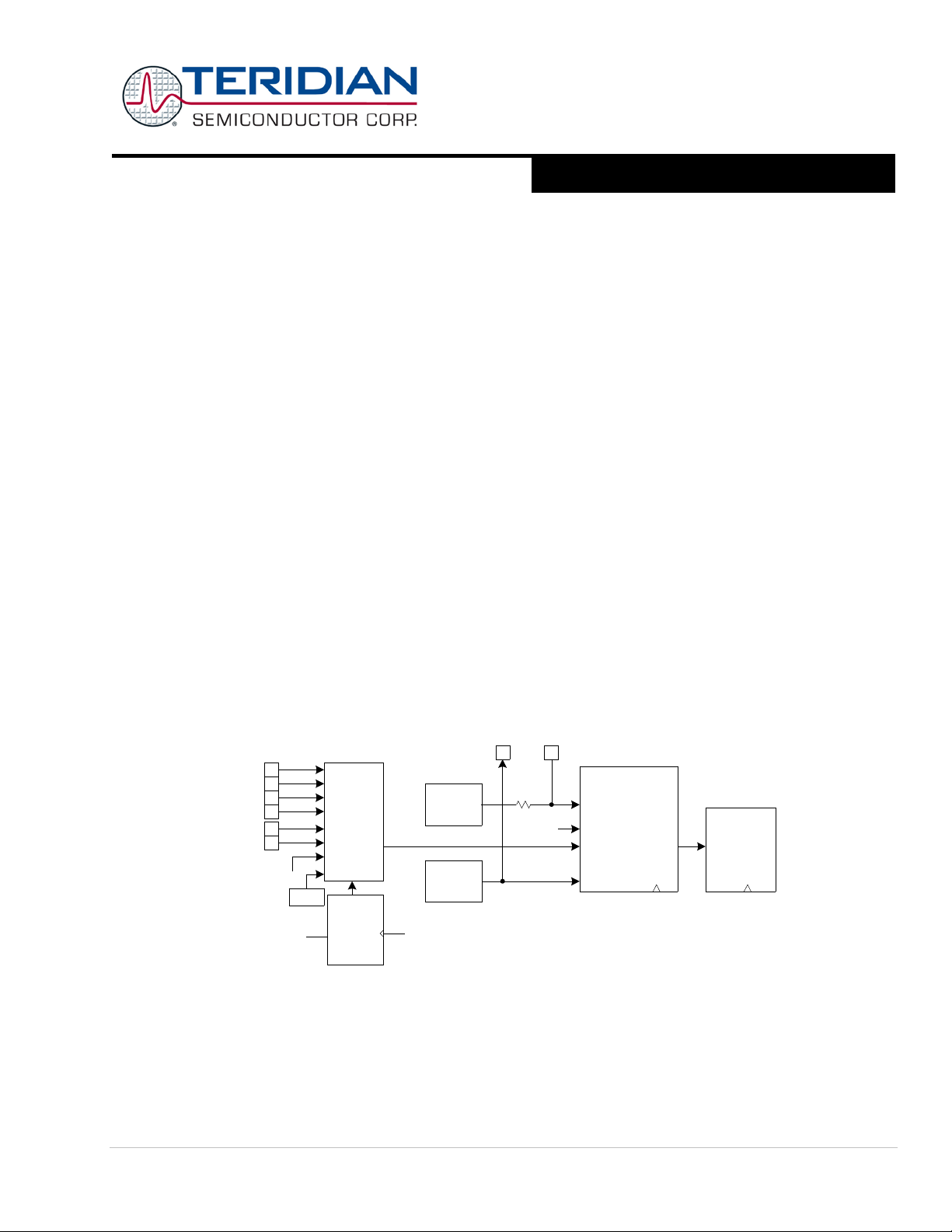
Figure 1: IC Functional Block Diagram
71M6513/71M6513H
3-Phase Energy Meter IC
DATA SHEET
A Maxim Integrated Products Brand
SEPTEMBER 2011
HARDWARE DESCRIPTION
Hardware Overview
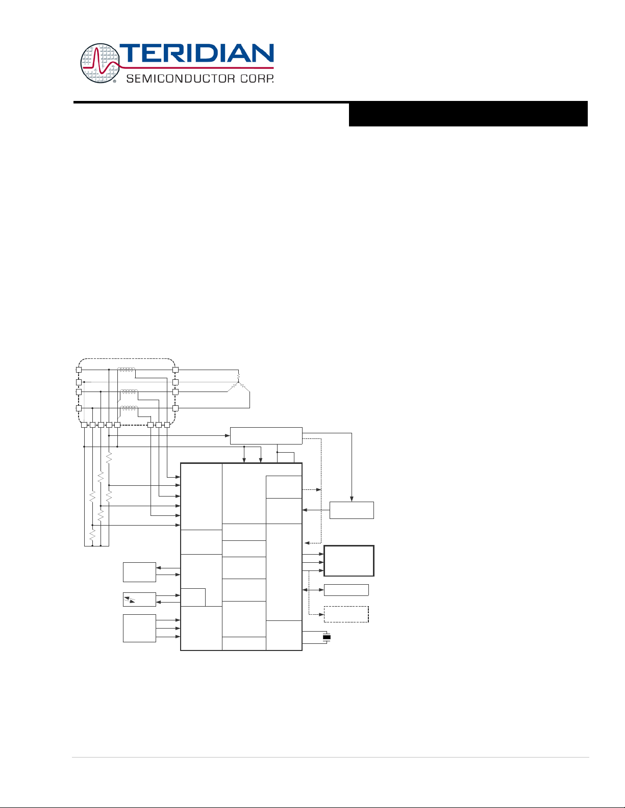
The 71M6513 single-chip polyphase meter integrates all primary functional blocks required to implement a solid-state
electricity meter. Included on chip are an analog front end (AFE), an 8051-com pa ti ble mi cr opr oc ess or ( MPU ) whi ch exec ut es
one instruction per clock cycle (80515), an independent 32-bit digital computation engine (CE), a voltage reference, a
tem peratur e senso r, LCD driver s, RAM, flash memory, a real time clock (RTC), and a variety of I/O pins. Various current
sensor technologies are supported including Curre nt Transfo r mers (CT), Resistive Shunts, and Rogowski (di/dt) Coils.
In addition to advanced m easurement functions, the real time clock function allows the 71M6513/6513H to record tim e of use
(TOU) metering information for multi-rate applications. Measurements can be displayed on either a 3V or a 5V LCD. Flexible
mapping of LCD display segments will facilitate integration with any LCD format. The design tr ade-off b et w een t h e n u m ber o f
LCD segments and DIO pins can be flexibly configured using memory-mapped I/O to accommodate various requirements.
The 71M6513 includes several I/O peripheral functions that improve the functionality of the device and reduce the component
count for most meter applications. The I/O peripherals include two UARTs, digital I/O, comparator inputs, LC D displ ay driver s ,
2
C int erface and an optic al/IR i nterf ace.
I
One of the two internal UARTs (UART1) is adapted to support an Infrared LED with internal drive output and sense input but it
can also function as a standard UART.
A block diagram of the chip is shown in Figure 1. A det ailed description of va r ious hardware blocks fol lows.
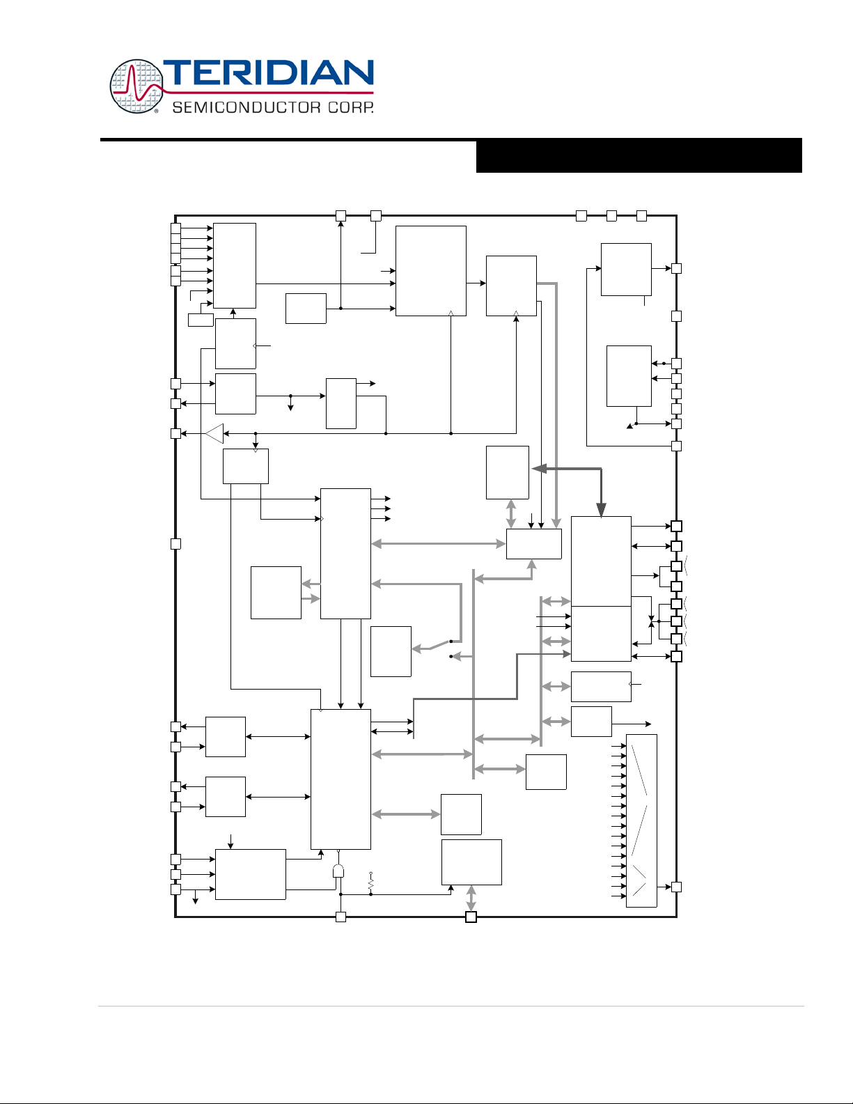
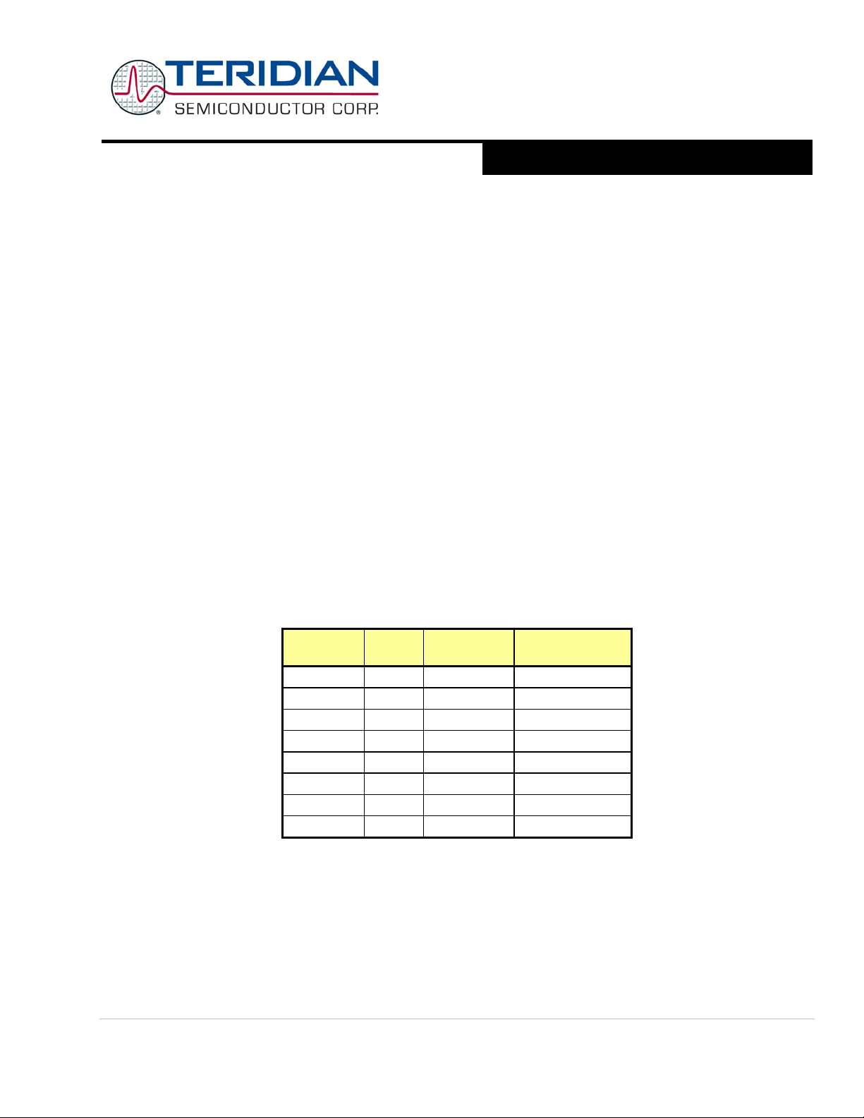
Analog Front End (AFE)
The AFE of the 71M6513 Power Meter IC is comprised of an input m ulti plexer, a del ta-sigma A/D converter with a voltage
ref erence, fol lowed by an FI R filter . A block diagram of t he AFE is shown i n Figure 3.
Multiplexer
The input multiplexer support s eight input signals that are applied to the pins IA, VA, IB, VB, IC, VC, and V3 plus the output of
the inter nal tempera ture sensor. The multiplexer can be operated in tw o modes:
• Dur ing a nor mal mu l tiplexer cycle, t he signals from the six pi ns IA, VA , IB, VB, IC, and VC are s elect ed.
• During the alternate multiplexer cycle, the temperature signal (TEMP) and the additional monitor input, V3, are
selected, along with the other signal sources shown in Table 1: I nputs Selected in Regular and Alternate Multiplexer
Cycles.
Alt er nat e mul ti pl exer cy cles ar e us ual ly perf or m ed inf req uent l y (ev er y sec on d or so) . VA , VB , an d VC a re n ot r epl ac ed i n th e
alternate multiplexer cycles. In some equations, currents must be delayed in allpass networks and therefore cannot be
repl ac ed in th e al tern ate sel ect ion . Mis sin g sampl es du e to al tern ate m ulti plexer cyc les are a utomat ica lly i nter polated by the
CE.
Regular multiplexer sequence
Mux State:
0 1 2 3 4 5 0 1 2 3 4 5
IA VA IB VB IC VC TEMP VA V3 VB IC VC
Table 1: Inputs Selected in Regular and Alternate Multiplexer Cycles
In a typical application, the IA, IB, and IC inputs are connected to current transformers that sense the current on each phase of
the line voltage. VA, VB, and VC are typically connected to voltage sensors through resistor dividers.
The Multiplexer Control Circuit handles the setting of the multiplexer. The function of the Multiplexer Control Circuit is
governed by the I/O RAM registers MUX_ALT (0x2005[2]), EQU (0x2000[7:5]), and MUX_DIV (0x2002[7:6]). MUX_DIV controls
the number of samples per cycle. It can requ est 2, 3, 4, or 6 multiplexer states per cycle.
Alternate multiplexer sequence
Mux State:
© 2005-2011 Teridian Semiconductor Corporation Page: 9 of 104
71M6513/71M6513H
3-Phase Energy Meter IC
DATA SHEET
A Maxim Integrated Products Brand
G
-
+V
inp
V
outp
V
outn
V
inn
CROSS
A
B
A
B
A
B
A
B
AUGUST 2011
The MUX_ALT bit requests an alternate multiplexer cycle. The bit may be asserted on any MPU cycle and may be subsequently de-asserted on any cycle including the next one. A rising edge on MUX_ALT will cause the Control Circuit to wait
until the next multiplexer cycl e and implement a sin gle alternate cycle.
Multiplexer Control Circuit also controls the FIR filt er initiation and the chopping of the ADC reference voltage, VREF. The
Mult iplexer Contro l Circuit is clocked by CK32, the 32768Hz clock from the PLL block, and launches each pass through the CE
program.
ADC
A single 21/22 -bit delta-sigma A/D converter digitizes the power inputs to the AFE. The resolution of the ADC is programmable
usi ng t he I/O RAM r egist er FIR_LEN register (0x2005[4]). ADC resolution may be selected to be 21 bits (FIR_LEN=0), or 22
bits (FIR_LEN=1). Convers ion time is tw o cycles of CK 32 with FIR_LEN = 0 and three cyc les wit h FIR_LEN = 1.
Accuracy, timing and functional spec ificatio ns in this data sheet are based on FIR_LEN = 0 (two CK32 cyc les).
Initiation of each ADC conversion is controlled by the Multiplexer Control Circuit as described previously.
FIR Filter
The finite impulse response (FIR) filter is an integral part of the ADC and it is optimized for us e with th e m ultipl exer. The
purpose of the FIR is to decimate the ADC output to the desired resolution. At the end of each ADC conversion, the output
data of the FIR filter (raw data) is stored into the CE DRAM location determined by the multiplexer selec ti o n. T he l oc ati on o f
the raw data in the CE DRAM is specified in the CE Program and Environment Section.
Voltage Reference
The 71M6513/6513H includes an on-chip precision bandgap voltage reference that incorporates auto-zero techniques. The
reference of the 71M6513H is trimm ed in production to minimize errors caused by component mismatch and drift. The result is
a voltage output with a predictable temperature coefficient.
The voltage reference is chopper stabilized, i.e. the polarity can be switched by the MPU using the I/O RAM register CHOP_EN
(0x2002[5:4]). The two bits in the CHOP_EN register enable the MPU to operate the chopper circuit in regular or inverted
operation, or in “toggling” mode. When the chopper circuit is toggled in between multiplexer cycles, DC offsets on the
measured signals will automatically be averaged out.
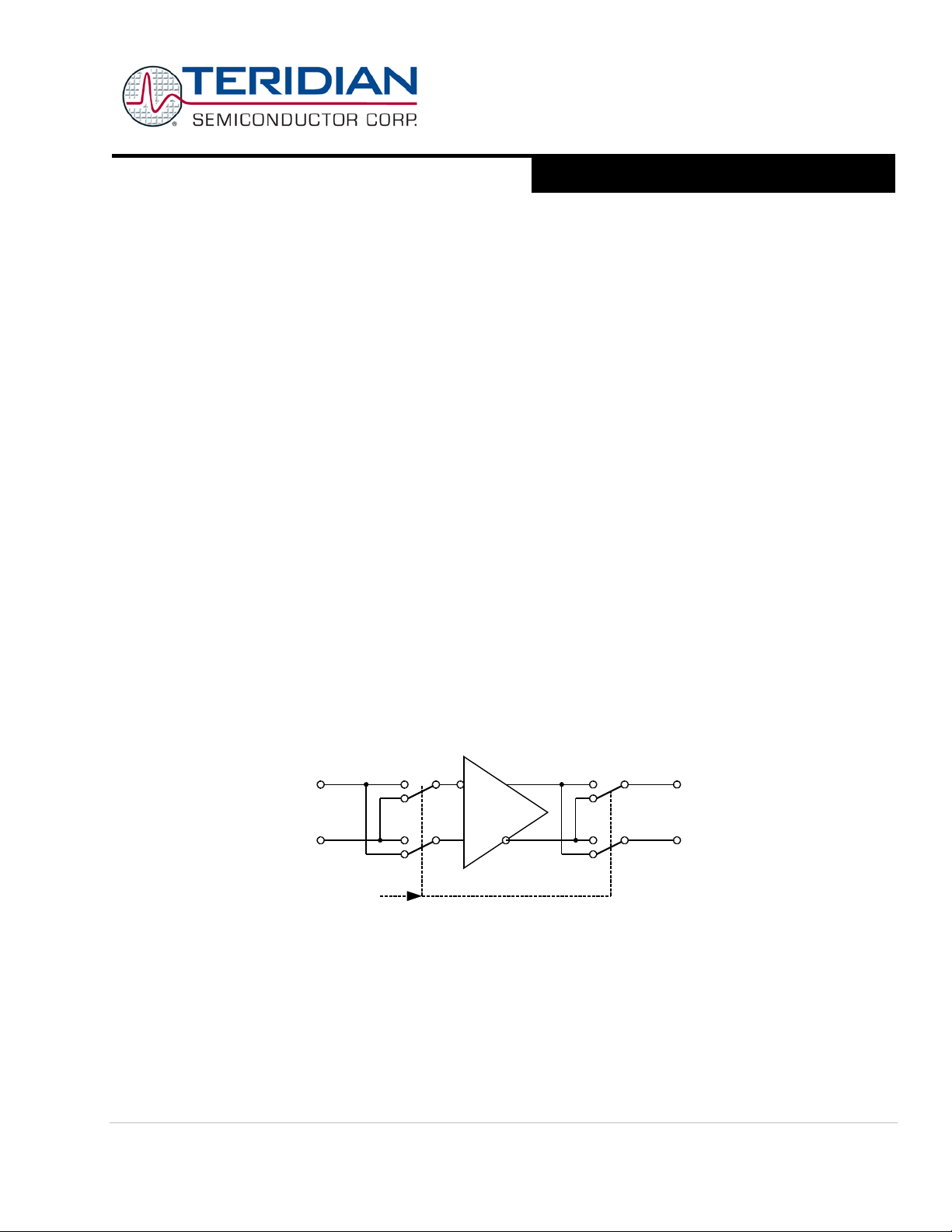
The general t opology of a chopped amplifier is given in Figure 2.
Figure 2: General Topology of a Chopped Amplifier
It is assumed that an offset voltage Voff appears at the positive amplifier input. With all switches, as controlled by CROSS in
the “A” position, the output voltage is:
Voutp – Voutn = G (Vinp + Voff – Vinn) = G (Vinp – Vinn) + G Voff
Page: 10 of 104 © 2005-2011 Teridian Semiconductor Corporation
71M6513/71M6513H
3-Phase Energy Meter IC
DATA SHEET
A Maxim Integrated Products Brand
IA
VA
IB
VB
MUX
VREF
VBIAS
IC
VBIAS
(1.5V)
TEMP
CK32
VREF
VREF_DIS
MUX
CTRL
MUX_DIV
CHOP_EN
EQU
VC
MUX
V3
MUX_ALT
V3P3A
FIR_LEN
FIR
FILTER
∆Σ ADC
CONVERTER
+
-
VREF
SEPTEMBER 2011
With all switches set to the “B” position by applying the inverted CROSS signal, the output voltage is:
Voutn – Voutp = G (Vinn – Vinp + Voff) = G (Vinn – Vin p) + G Voff, or
Voutp – Voutn = G ( Vinp – Vinn) - G Voff
Thu s, when C ROSS i s toggled, e.g. af ter each multiplex er cyc le, the offset wil l alternately appear on the o utput as positiv e and
nega tiv e, which results in the offset ef fectively b eing el iminated, r egardless of its po larity or magnitu de.
The Functional Description Sec tion c ontains a ch apter with a det ailed description on control lin g t he CHOP_EN register.
Temperature Senso r
The 71M6513/6513H includes an on-chip temperature sensor implemented as a bandgap r efer ence. It i s us ed to determine
the die temperature The MPU may request an alternate multiplexer cycle containing the temperature sensor output by
asserting MUX_ALT.
The primary use of the temperature data is to determine the magnitude of compensation required to offset the thermal drift in
the system (see sec tio n t i tled “ Temperature Compensation”).
The z ero reference for the tem perature sen sor i s VBIAS.
V3
V3 is an additional analog monitor input that can be used for analog measurements, such as neutral current. It is sampled
when the multiplexer p erforms an alternate multiplexer cycle. The z ero reference for the V3 input is V BIAS.
V3 is also routed into the comparator block where it is compared to VBIAS. Comparator interrupts should be disabled when
the V3 input is used for analog measurements.
Functional Description
The AFE functions as a data acquisition system, controlled by the MPU. The main signals (IA, VA, IB, VB, IC, VC) are
sampled and the ADC counts obtained are stored in CE RAM where they can be accessed by the CE and, if necessary, by the
MPU. Alternate multiplexer cycles are initiated less frequently by the MPU to gather access to the slow signals, temperature
and V3.
© 2005-2011 Teridian Semiconductor Corporation Page: 11 of 104
Figure 3: AFE Block Diagram
71M6513/71M6513H
3-Phase Energy Meter IC
DATA SHEET
A Maxim Integrated Products Brand
0x00
IA
V3P3
Pha se A cur rent
0x02
IB
V3P3
Pha se B cur rent
AUGUST 2011
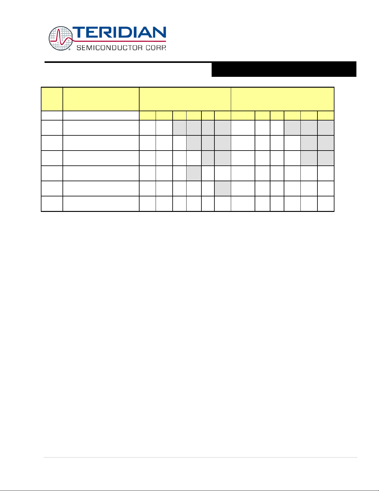
Computation Eng ine (CE)
The CE, a dedicated 32-bit RISC processor, performs the precision computations necessary to acc urately m easure energy.
The CE calculations and processes include:
• Multiplication of each current sample with its associated voltage sample to obtain the energy per sample (when
multiplied with the constant sample time).
• Frequency-insensitive delay cancellation on all six channels (to compensate for the delay between samples caused
by the multiplexing scheme).
• 90° phase shifter (for VAR calculati ons).
• Pulse generation.
• Monitoring of the input signal frequency (for frequency and phase information).
• Monitoring of the input signal amplitude (for sag detection).
• Scaling of the processed samples based on chip temperature (temperature compensation) and calibration
coefficients.
The CE program RAM (CE PRAM) is loaded at boot time by the MPU and then executed by the CE. Each CE instruction word
is 2 bytes long. The CE program counter begins a pass through the CE code each time multiplexer state 0 begins. The code
pass ends when a HALT instruction is executed. For proper operation, the code pass must be completed before the
mul tiplexer cycle ends (see System Timing Summary in the Fun ctio nal Des cription Sec tion) .
The CE data RAM (CE DRAM) can be accessed by the FIR filter block, the RTM circuit, the CE, and the MPU. Assign ed time
sl ots are reserved for FIR, R TM, and MPU, respectively, such that m emory access es to CE_RAM do not collide. Holdi ng registers are used to convert 8-bit wide MPU data to/ from 32-bit wide CE DRAM data, and wait states are inserted as needed,
depending on the frequency of CKMPU.
Table 2 shows the CE DRAM addresses allocated to analog inputs from the AFE.
Address Name
0x01 VA V3P3 Phase A voltage
0x03 VB V3P3 Phase B voltage
0x04 IC V3P3 Phase C current
0x05 VC V3P3 Phase C voltage
0x06 TEMP VBIAS Temperature
0x07 V3 VBIAS V3 monitor
Table 2: CE DRAM Locations for ADC Results
Zero
Reference
Description
Meter Equations
The Compute Engine (CE) program for industrial m eter configurations implements the equations in Table 3. The I/O RAM
register EQU specifies the equation to be used based on the number and arrangement of phases used for metering. In case of
single and two-phase metering, the unconnected inputs should be tied to V3P3A, the analog supply voltage. The EQU
selection enables the 71M6513 to calculate polyphase power measurement based on the type of service used. Table 3 also
states t he sequence of t he multipl exer in t he AFE.
Page: 12 of 104 © 2005-2011 Teridian Semiconductor Corporation
71M6513/71M6513H
3-Phase Energy Meter IC
DATA SHEET
A Maxim Integrated Products Brand
(1 element, 2W 1ø)
(1 element, 3W 1ø)
(2 element, 4W 3ø Delta)
(3 element, 4W 3ø Wye)
SEPTEMBER 2011
EQU
Watt & VAR Formula
0 1 2 3 4 5 0 1 2 3 4 5
VA IA
0
VA(IA-IB)/2
1
VA IA + VB IB
2
(2 element, 3W 3 øDelta)
VA (IA - IB)/2 + VC IC
3
VA(IA-IB)/2 + VB(IC-IB)/2
4
(2 element, 4W 3ø Wye)
VA IA + VB IB + VC IC
5
Table 3: Standard Meter Equations (inputs shown gray are scanned but not used for calculation)
Inputs used from MUX sequence
Mux State:
IA VA IB VB IC VC TEMP VA V3 VC IC VC
IA VA IB VB IC VC TEMP VA IB V3 VC VC
IA VA IB VB IC VC TEMP VA V3 VB VC VC
IA VA IB VB IC VC TEMP VA IB V3 IC VC
IA VA IB VB IC VC TEMP VA IB V3 IC VC
IA VA IB VB IC VC TEMP VA V3 VB IC VC
Inputs used from alternate MUX
sequence
Mux State:
Pulse Generator
The CE contains two pul se generato rs which cr eate low jitter pulses at a rate set by the CE D RAM reg isters APULSEW*WRATE
and APULSER*WRATE if EXT_PULSE (a CE input variable in CE DRAM) is 15. This mode puts the MPU in control of pulse
generation by placing values into the APULSEW and APULSER register s (“external puls e genera tio n”).
If EXT_PULSE is 0, APULSEW i s replaced with WSUM_X and APULSER is repla ced wit h VARSUM_X. In t his m ode, the CE
generates pulse based on its internal computation of WSUM_X and VARSUM_X, the signed sums of energy from all three
elements (“internal pulse generation”).
The DIO_PV and DIO_PW bit s as described in the Digital I/O section can be programmed to route W PULSE and VARPULSE
to the output pins DIO6 and DIO7 respectively. DIO6 and DIO7 can be configured to generate int errupts, which can be useful
for pulse counting by the MPU (see On-Chip Res ourc es, DIO Po rts sectio n).
Real-Time Monit or
The CE contains a Real Time Monitor (RTM), which can be programmed to monitor four selectable CE RAM l o cati on s at f ul l
sam ple rat e. The fo ur moni tored l ocatio ns are ser iall y output to the TM UXOUT pi n via t he digit al outp ut multi plexer at the
beginning of each CE code pass (see the Tes t Port s Section for details)
CE Functional Overview
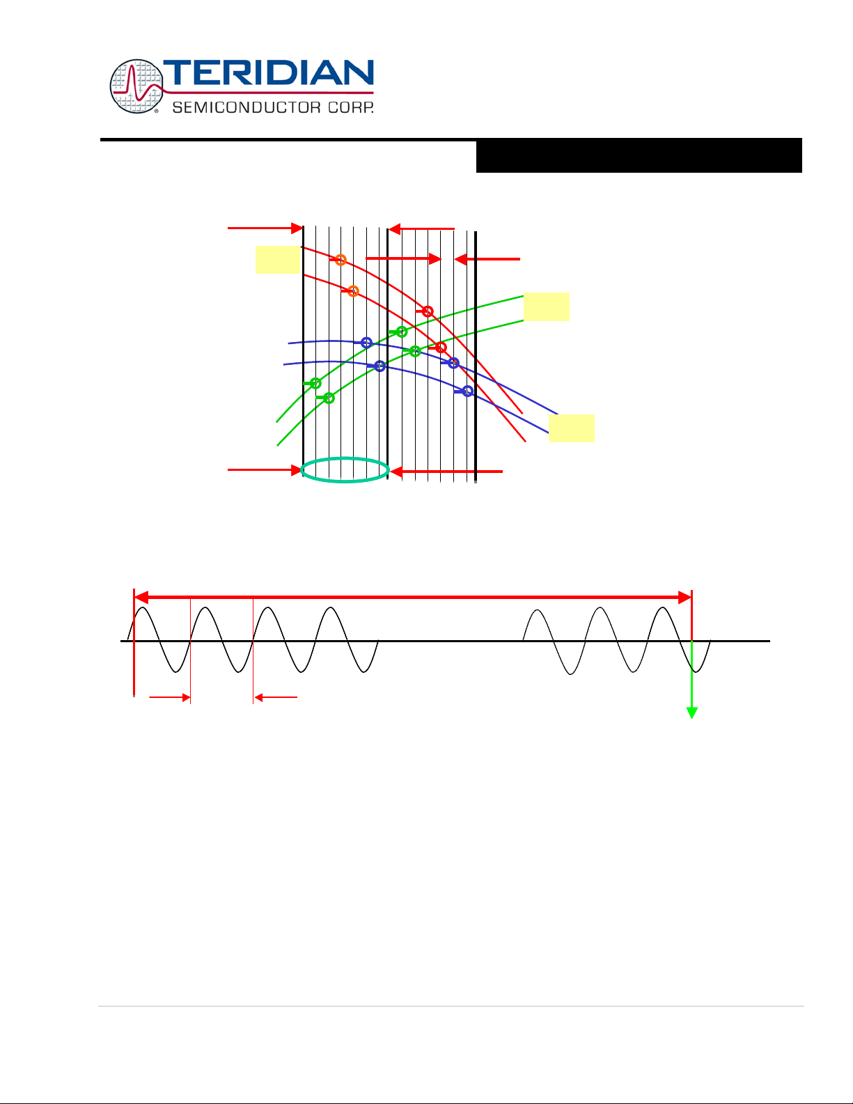
The ADC processes on e sample p er c h an n el p er mul t i pl exer cy cl e. Figure 4 shows the timing of the six samples taken during
one multiplexer cycle.
The number of samples processed during one accumulation cycle is controlled by the I/O RAM registers PRE_SAMPS
(0x2001[7:6]) and SUM_CYCLES (0x2001[5:0]). The integration time for each energy output is
PRE_SAMPS * SUM_CYCLES / 2520.6, w here 25 20.6 i s the sample rate [Hz]
For examp le, PRE_SAMPS = 42 and SUM_CYCLES = 50 wil l establish 2100 samples per accumulati on cycle. PRE_SAMPS = 100
and SUM_CYCLES = 21 will res ult i n the exa ct s ame acc umulat ion c ycle of 2100 s amples or 833m s. Aft er an accumul ation
cycle is c omplet ed, th e X FER_B U SY interrupt sig nals to the MPU that accumulated da ta are avail able.
© 2005-2011 Teridian Semiconductor Corporation Page: 13 of 104
71M6513/71M6513H
3-Phase Energy Meter IC
DATA SHEET
A Maxim Integrated Products Brand
VA
VB
IB
VC
IC
IA
1/2520.6Hz = 397µs
2/32768Hz =
61.04µs
13/32768Hz = 397µ s
per mux cycle
A
C
B
VA
VB
IB
VC
IC
IA
1/2520.6Hz = 397µs
2/32768Hz =
61.04µs
13/32768Hz = 397µ s
per mux cycle
A
C
B
XFER_BUSY
Interrupt to MPU
20ms
833ms
XFER_BUSY
Interrupt to MPU
20ms
833ms
AUGUST 2011
Figure 4: Sam ples in M ultip lexer C ycle
The en d of ea ch mul tiplex er cy cle is si gnal ed to t he MPU by the CE_ BUSY i nterr upt. At the end o f each m ultip lexer c ycl e,
status i nformation, such as sag data and the digitized input signal, is available to the MPU.
Figure 5 shows the accumulation interval resulting from PRE_SAMPS = 42 and SUM_CYCLES = 50, consisting of 2100 samples
of 397µs each (only one phase is shown) followed by the XFER_BUSY interrupt. The sampling in this example is applied to a
50Hz signal.
Ther e is no c orr el ati on bet ween t he l i ne si gn al fr equ enc y a nd t he ch oi ce of PRE_SAMPS or SUM_CYCLES (even though when
SUM_CYCLES = 42 one set of SUM_CYCLES happens to sample a period of 16.6ms). Furtherm or e, s am pl i ng d oes n ot h ave t o
start when the line voltage crosses the zero line.
Delay Compensation
When measuring the energy of a phase (i.e., Wh and VARh) in a service, the voltage and current for that phase must be
sampled at the same instant. Other w ise, the phase difference, Ф, introduces errors.
Page: 14 of 104 © 2005-2011 Teridian Semiconductor Corporation
Figure 5: Accumulation Interval

71M6513/71M6513H
3-Phase Energy Meter IC
DATA SHEET
A Maxim Integrated Products Brand
o
delay
o
delay
ft
T
t
360360 ⋅⋅=⋅=
φ
SEPTEMBER 2011
Where f is the frequency of the input signal and t
In traditional meter ICs, sampling is accomplished by using two A/D converters per phase (one for voltage and the other one
for current) controlled to sample simultaneously. Our Single-Converter Technology, however, exploits the 32-bit signal
processing capability of its CE to implement “constant delay” all-pass filters. These all-pass filters correct for the conversion
time difference between the voltage and the corresponding current samples that are obtained with a single multiplexed A/D
converter.
The “constant delay” all-pass filters provide a broad-band delay β that is precisely matched to the difference in sam ple t im e
between the voltage and the current of a given phase. This digital filter does not affect the amplitude of the signal, but
pro vi des a prec i sel y co ntr oll ed p ha se r esp ons e. T he del a y com pen sat ion imp lem ent ed i n th e CE al i gns the v ol ta ge s ampl es
with their corresponding current samples by routing the voltage samples through the all-pass filter, thus delaying the voltage
samples by β, resulting in the residual phase error β – Ф. The residual phase error is negligible, and is typically less than ±1.5
milli-degrees at 100Hz, thus it does not contribute to errors in the energy measurements.
is th e sampling delay between voltage and current .
delay
© 2005-2011 Teridian Semiconductor Corporation Page: 15 of 104
71M6513/71M6513H
3-Phase Energy Meter IC
DATA SHEET
A Maxim Integrated Products Brand
0xFFFF
0xFFFF
0x4000
0x3FFF
0x3000
0x2FFF
0x2100
0x20FF
0x2000
0x1FFF
0x1400
0x13FF
0x1000
0x0FFF
0x0800
0x07FF
0xFF
SFRs, RAM,
reg. banks
0x0000
0x0000
0x00
AUGUST 2011
80515 MPU Core
80515 Overview
The 71M6513/6513H includes an 80515 MPU (8-bit , 8051 -compatible) that processes most instructions in one clock cycle.
Using a 5MHz clock results in a processing throughput of 5 MIPS. The 80515 architecture eliminates redundant bus s ta tes and
implements parallel execution of fetch and execution phases. Normally a machine cycle is aligned with a memory fetch, therefore, most of the 1-byte instructions are performed in a single cycle. This leads to an 8x performance (in average)
improvement (in terms of MIPS) over t he Intel 8051 device running at t he sam e clock frequency.
Actual processor clocking speed can be adjusted to the total processing demand of the application (metering calculations,
AMR management, memory management, LCD driver management and I/O management) using the I/O RAM register
MPU_DIV[2:0].
Typical measurement and metering functions based on the results provided by the internal 32-bit com pute eng ine ( CE) are
available for the MPU as part of Teridian’s standard library. A standard ANSI “C” 80515-application programming interface
library is avai labl e to help reduce desi gn cycle.
Memory Organization
The 80515 MPU core incorporates the Harvard architecture with separate code and data spaces.
Memory organization in the 80515 is similar to that of the industry standard 8051. There are three memory areas: Program
memo ry (flash), external data memory (XRAM), physically consisting of XRAM, CE DRAM, CE PRAM and I/O RAM, and
internal data memory (Internal RAM). Figure 6 shows the memory map (see also Table 54).
Int er n al a nd Extern al D at a M em or y: Both internal and external data memory are physically located on the 71M6513 IC. External data memory is only external to the 80515 MPU core.
Flash memory
Progra m me mory External data memory Internal data memory
Progra m Memo ry: The 80515 can address up to 64KB of program memory space from 0x0000 to 0xFFFF. Program memory
is read when the MPU fetches instructions or performs a MOVC operation.
After res et, th e M PU starts program execution from location 0x00 00. T he lower part of the p r ogram memor y incl udes reset an d
interru pt vectors. The int errupt vectors are spac ed at 8-byte intervals, starting from 0x0003.
Ext ernal Data Mem ory: W hile the 80515 can address up to 64KB of external data memory in the space from 0x0000 to
0xFFFF, only the memory ranges shown in Figure 6 contain physical memory. The 80515 writes into external data memory
Page: 16 of 104 © 2005-2011 Teridian Semiconductor Corporation
---
CE PRAM
---
I/O RAM
---
CE DRAM
---
XRAM
Figure 6: Memory Map
71M6513/71M6513H
3-Phase Energy Meter IC
DATA SHEET
A Maxim Integrated Products Brand
0 0 1 1 2 2 3
1
SEPTEMBER 2011
when the MPU executes a MOVX @Ri,A or MOVX @DPTR,A i nstruction. The MPU reads external data memory by executing
a MOVX A,@Ri or M OVX A,@DPTR instruction (SFR USR2 provides the upper 8 bytes for the MOVX A,@Ri instruction).
Clock Stretching: MOVX instructions can access fast or slow external RAM and external peripherals. The three low ordered
bits of the CKCON register define the stretch memory cycles. Setting all the CKCON st retch bits to one allows access to very
sl ow extern al RA M or exter nal peripherals.
Table 4 shows how the signals of the Ex ternal Memory Interface change when stretch values are set from 0 to 7. The widths of
the signals are counted in MPU clock cycles. The post-reset state of the CKCON register, which is in bold in the table,
performs the MOVX instructions with a stretch value equal to 1.
CKCON register Stretch Value Read signals width Write signal width
CKCON.2 CKCON.1 CKCON.0 memaddr memrd memaddr memwr
0 0 0 0 1 1 2 1
0 1 0 2 3 3 4 2
0 1 1 3 4 4 5 3
1 0 0 4 5 5 6 4
1 0 1 5 6 6 7 5
1 1 0 6 7 7 8 6
1 1 1 7 8 8 9 7
Table 4: Stretch M emory C ycle Width
There are two types of instructions, differing in whether they provide an eight-bit or s i xteen-bit indirect address to the external
data RAM.
In the first type (MOVX A,@Ri), the contents of R0 or R1, in t he current regist er bank, provide the eight l ower-ordered bits o f
address. The eight high-ordered bits of address are specified with the USR2 SFR. This method allows the user paged access
(256 pages of 256 bytes each) to the full 64KB of external data RAM. In the second type of MOVX instruction (MOVX
A,@DPTR), the dat a po i nt er g en er at es a s i xt een -bit address. This form is faster and more efficient when accessing very large
data arrays (up to 64 Kbytes), since no additional instructions are needed to set up the eight high ordered bits of address.
It is possible to m ix t he t wo MO VX t ypes . T his p rov id es t he us er wi th four s epar at e dat a p oint er s, t wo wi th d ir ect acc ess a nd
two with paged access to the entire 64KB of external memory range.
Dual Data Pointer: The Dual Data Pointer accelerates the block moves of data. The standard DPTR is a 16-bit register that i s
used to address external memory or peripherals. In the 80515 core, the standard data pointer is call ed DPTR, the second data
pointer is called DPTR1. The data pointer select bit chooses the active pointer. The dat a pointer select bit is locat ed at the LSB
of the DPS register (DPS.0). DPTR is selected when DPS.0 = 0 and DPTR1 is selected when DPS. 0 = 1.
The user switches between pointers by toggling the LSB of the DPS regi ster . A ll DPTR-related instructions use the currently
selected DPTR for any activity.
The second data pointer may not be supported by certain compilers.
© 2005-2011 Teridian Semiconductor Corporation Page: 17 of 104
71M6513/71M6513H
3-Phase Energy Meter IC
DATA SHEET
A Maxim Integrated Products Brand
Address
Direct ad dressing
Indirect addressing
0x20
0x00
X000
X001
X010
X011
X100
X101
X110
X111
F8
INTBITS
FF
F0 B
F7
E8
WDI EF
E0 A
E7
D8
WDCON
DF
D0
PSW D7
C8
CF
C0
IRCON C7
B8
IEN1
IP1
S0RELH
S1RELH USR2
BF
B0
FLSHCTL
PGADR
B7
A8
IEN0
IP0
S0RELL
AF
A0
P2
DIR2
DIR0 A7
98
S0CON
S0BUF
IEN2
S1CON
S1BUF
S1RELL
EEDATA
EECTRL
9F
90
P1
DIR1
DPS
ERASE 97
88
TCON
TMOD
TL0
TL1
TH0
TH1
CKCON
8F
80
P0
SP
DPL
DPH
DPL1
DPH1
WDTREL
PCON
87
AUGUST 2011
Int ernal Data Mem ory: The Internal data memory provides 256 bytes (0x00 to 0xFF) of data memory. The internal data
memory address is always 1 byte wide and can be accessed by either dir ect or indirect addressing. The Special Function
Registers occupy the upper 128 bytes. This SFR area is available only by direct addressing. Indirect addressing
accesses the upper 128 bytes of Internal RAM.
The lower 128 bytes contain working registers and bit-addressable memory. The lower 32 bytes form four banks of eight
registers (R0-R7). Two bits on the program memory status word (PSW) select which bank is in use. The next 16 bytes form a
blo ck of bit -addressa bl e memor y sp ace a t bi t add ress ees 0 x00-0x7F. All of the bytes in the lower 128 bytes are accessible
through direct or indirect addressing. Table 5 shows the internal data memory map.
0xFF
0x80
0x7F
0x30
0x2F
0x1F
Special Function Registers
(SFRs)
Byte-addressable area
Bit-ad dressable area
Register banks R0…R7
Table 5: Internal Data Memory Map
Special Function Regi st ers ( SFRs)
A map of the Special Function Registers is shown in Table 6.
Hex\Bin
Bit-address-
able
Byte-addressable
RAM
Bin/Hex
Table 6: Special Function Registers Locations
Only a few addresses are occupied, the others are not impl emented. SFRs specific to the 651X are shown in bold print. Any
read access to unimplemented addresses will return undefined data, while any w r i t e a cc es s wi l l h a ve n o ef f ec t . Th e r eg i s t er s
at 0x80, 0x88, 0x90, etc., are bit-addres sable, all others are byte-addressable.
Page: 18 of 104 © 2005-2011 Teridian Semiconductor Corporation
71M6513/71M6513H
3-Phase Energy Meter IC
DATA SHEET
A Maxim Integrated Products Brand
P0
0x80
0xFF
Port 0
SP
0x81
0x07
St ack Poi nter
DPL
0x82
0x00
Data Pointer Lo w 0
DPH
0x83
0x00
Data Pointer High 0
DPL1
0x84
0x00
Data Pointer Lo w 1
DPH1
0x85
0x00
Data Pointer High 1
WDTREL
0x86
0x00
Watchdog Timer R eload register
PCON
0x87
0x00
UART Speed Control
TCON
0x88
0x00
Timer/Counter Control
TMOD
0x89
0x00
Timer Mode Control
TL0
0x8A
0x00
Timer 0, low byte
TL1
0x8B
0x00
Timer 1, high byte
TH0
0x8C
0x00
Timer 0, low byte
TH1
0x8D
0x00
Timer 1, high byte
CKCON
0x8E
0x01
Clock Control (Stretch=1)
P1
0x90
0xFF
Port 1
DPS
0x92
0x00
Data Pointer select R egist er
S0CON
0x98
0x00
Serial P or t 0, Con trol R egist er
S0BUF
0x99
0x00
Serial P or t 0, Data Buffer
IEN2
0x9A
0x00
Interrupt Ena ble Register 2
S1CON
0x9B
0x00
Serial P or t 1, Con trol R egist er
S1BUF
0x9C
0x00
Serial P or t 1, Data Buffer
S1RELL
0x9D
0x00
Serial P or t 1, Reload Regist er, low byte
P2
0xA0
0x00
Port 2
IEN0
0xA8
0x00
Interrupt Ena ble Register 0
IP0
0xA9
0x00
Interrupt Pri ority Regis ter 0
S0RELL
0xAA
0xD9
Serial P or t 0, Reload Regist er, low byte
P3
0xB0
0xFF
Port 3
IEN1
0xB8
0x00
Interrupt Ena ble Register 1
IP1
0xB9
0x00
Interrupt Pri ority Regis ter 1
S0RELH
0xBA
0x03
Serial P or t 0, Reload Regist er, hig h byte
S1RELH
0xBB
0x03
Serial P or t 1, Reload Regist er, hig h byte
Special Function Regi st ers ( Generic 80515 SFRs)
Table 7 shows the location of the SFRs and the value they assume at reset or power-up.
Name Location Reset value Description
SEPTEMBER 2011
© 2005-2011 Teridian Semiconductor Corporation Page: 19 of 104
71M6513/71M6513H
3-Phase Energy Meter IC
DATA SHEET
A Maxim Integrated Products Brand
Name
Location
Reset value
Description
USR2
0xBF
0x00
User 2 Port, high address byt e for MOVX@Ri
IRCON
0xC0
0x00
Interrupt Request Co ntrol Register
PSW
0xD0
0x00
Program Status Word
WDCON
0xD8
0x00
Baud Rate C ontrol Register (only WD CON.7 b it used )
A
0xE0
0x00
Accumulator
B
0xF0
0x00
B Reg ister
AUGUST 2011
Table 7: Special Function Registers Reset Values
Accumulator (ACC, A): ACC is the accumulator register. Most instructions use the accumulator to hold the operand. The
mnemonics for accumulator-sp ecific instructi ons refer to accumulator as “A”, not ACC.
B Register: The B register is used during multiply and divide instructions. It can also be used as a scratch-pad register to hold
temporary data.
Program Status Word (PSW):
MSB LSB
CV AC F0 RS1 RS OV - P
Table 8: PSW Register Flags
Page: 20 of 104 © 2005-2011 Teridian Semiconductor Corporation
71M6513/71M6513H
3-Phase Energy Meter IC
DATA SHEET
A Maxim Integrated Products Brand
PSW.7
CV
Carry flag
PSW.6
AC
in the
register.
RS1/RS0
Bank selected
Location
Parity flag, affected by hardware to indicate odd / even number of “one” bits in the
Bit Symbol Function
Auxiliary Carry flag for BCD operations
PSW.5 F0 G eneral purp ose Flag 0 available for user. Not to be confused with the F0 flag
CESTATUS
PSW.4 RS1 Register bank selec t control bits. The contents of RS1 and RS0 select the working
register bank:
SEPTEMBER 2011
PSW.3 RS0
PSW.2 OV Overflo w fla g
PSW.1 - User defined flag
PSW.0 P
Acc umulator, i .e. even pari ty.
Stack Pointer (SP): T he sta ck point er is a 1-byte regi ster ini tiali zed to 0x07 af ter r eset. This reg ister is inc remen ted befo re
PUSH and CALL instructions, causing the stack to begin at location 0x08.
Data Pointer: The data poi nter (DPTR) is 2 bytes wide. The lower part is DPL, and the highest is DPH. It can be loaded as a 2-
byt e r eg i st er ( MO V DPTR,# dat a 1 6) or as two r eg is t er s ( e. g . MOV DPL,#data8). It is generally used to access external code or
data space (e.g. MOVC A,@A+DPTR or MOVX A,@DPTR respectively).
Program Counter: The p rogram count er (PC) is 2 bytes wide initialized to 0x0000 after reset. This register is incremented
during the fetching operation code or when operating on data from program memory.
00 Bank 0 (0x00 – 0x07)
01 Bank 1 (0x08 – 0x0F)
10 Bank 2 (0x10 – 0x17)
11 Bank 3 (0x18 – 0x1F)
Table 9: PSW bit functions
© 2005-2011 Teridian Semiconductor Corporation Page: 21 of 104
71M6513/71M6513H
3-Phase Energy Meter IC
DATA SHEET
A Maxim Integrated Products Brand
P0
0x80
R/W
Register for port 0 read and write operations (pins DIO0…DIO7)
DIR0
0xA2
R/W
Data direction register for port 0. Setting a bit to 1 m eans that the corresponding pin is
an output.
P1
0x90
R/W
Register for port 1 read and write operations (pins DIO8…DIO15)
DIR1
0x91
R/W
Data direction register for port 1.
P2
0xA0
R/W
Register for port 2 read and write operations (pins DIO16…DIO21)
DIR2
0xA1
R/W
Data direction register for port 2.
ERASE
FLSH_ERASE
0x94
W
(default =
Any other pattern written to FLSH_ERASE will hav e no effect.
PGADDR
FLSH_PGADR
0xB7
R/W
Must be re-written for eac h new Pag e Eras e cycle.
EEDATA
0x9E
R/W
I2C EEPRO M i nterf ace data register
EECTRL
0x9F
R/W
I2C EEPRO M i nterf ace con t rol reg ist er . If th e M P U wish es to write a
0xB2
R/W
Bit 0 (FLSH_PWE): Pro gram Wri te Enable:
AUGUST 2011
Port Registers: The I/O ports are controlled by Special Function Registers P0, P1 , and P2. The contents of the SFR can be
observed on corresponding pins on the chip. Writing a ‘1’ to any of the ports (see Table 10) causes the corresponding pin t o
be at high level (V3P3), and writing a ‘0’ causes the corresponding pin to be held at low level (GND). The data direction
registers DIR0, DIR1, and DIR2 define individual pins as input or output pins (see section On-Chip Resou rces , DIO Ports for
details).
Register SFR
Address
All four ports on the chip are bi-directional. Each of them consists of a Latch (SFR ‘P0’ to ‘P3’), an output driver, and an input
buffer, therefore the MPU can output or read data through any of these ports. Even if a DIO pin is configured as an output, the
state of the pin can still be read by the MPU, for example when counting pulses issued via DIO pins that are under CE control.
R/W Description
Table 10: Port Registers
Special Function Regi st ers S pecific to the 71M6513
Table 11 shows the location and description of the 71M6513-specific SFRs.
Register Alternative
Name
SFR
Address
R/W Description
This register is used t o initiate either the Flash Mas s E rase cycle or
the Flash Page Er ase cycle. Specific patterns are expected for
FLSH_ERASE in or der to initiate the appr opriate Erase cycle
0x00).
0x55 – Initiat e Flash P age Erase cycle. Mus t be proc eeded by a write
to FLSH_PGADR @ SFR 0xB7.
0xAA – Initiate Flas h M ass Er ase cycle. Mus t be proceeded by a
wri te to FLSH_MEEN @ SFR 0xB2 and the debug port must
be enabled.
Flash Page Erase Address register containing the flash memory
page address (page 0 thru 127) that will be erased during the Page
Erase cycle (default = 0x00).
byte of data to EEPROM, it plac es the d ata in EEDATA and then
writes the ‘Transm it’ code to EECTRL. The write to EECTRL initiates
the transmit sequence. See the section
a description of the command and status bits available for EECTRL.
Page: 22 of 104 © 2005-2011 Teridian Semiconductor Corporation
0 – MOVX commands refer to XRAM Space, normal operation
(default).
I2C Interface (EEPROM) for
71M6513/71M6513H
3-Phase Energy Meter IC
DATA SHEET
A Maxim Integrated Products Brand
1 – MOVX @DPTR,A moves A to Program Space (flash) @ DPTR.
WDI 0xE8
Only byte operations on the whole WDI register should be used
The W DT is reset wh en a 1 is wri tten t o this b it.
INTBITS
INT0…INT6
0xF8
R
Interrupt inputs. The MPU may read these bits to see the input to
any memory and are primarily intended for debug use
SEPTEMBER 2011
Register Alternative
Name
SFR
Address
R/W Description
This bit is automatic ally reset after each byte written to flash. Writes
to this bit are inhibited when interrupts are enabled.
Bit 1 (FLSH_MEEN): Mass Eras e Enabl e:
W
0 – Mass Erase disabled (default).
1 – Mass Erase enabled.
Must be re-written for eac h new Mass Eras e c ycle.
Bit 6 (SECURE):
Enables security provisions that prevent external reading of flash
R/W
memory and CE program RAM. This bit is reset on chip reset and
may only be set. At tempt s to wri te zero are ig nored.
Bit 7 (PREBOOT):
R
Indicat es that the preboot s equence is act ive.
when writing. The b y te must have all bits set except the bits t hat are
to be cleared.
R/W
The multi-pur pose register WDI contains the fol lowing bits :
Bit 0 ( IE_XFER): XFER Interrupt Flag:
This flag monitors the XFER _BUSY in terru pt. It i s set by hardware
R/W
and must be cleared by the interrupt han dler
Bit 1 ( IE_RTC): RTC Interrupt Flag:
This flag monitors the RTC_1SEC interrupt. It is set by hardware and
W
must be cl eared by the interrupt handler
Bit 7 (WD_RST): W D Timer Reset:
Table 11: Special Function Registers
Instruction Set
All instructions of the generic 8051 microcontroller are supported. A complete li st of the instruction set and of the associated
op-codes is contained in the 651X Software User’s Guide (SUG).
UART
The 71M6513 includes a UART (UART0) that can be programmed to communicate with a variety of AMR modul es . A s eco n d
UART (UART1) is connected to the optical port, as described in the optical port description.
The UART is a dedicated 2-wire serial interface, which can communicate with an external host processor at up to 38,400 bits/s
((with MPU clock = 1.2288MHz). The operation of each pin is as follows:
RX: Serial input data ar e applied at this pin. Conforming to RS-232 standard, the bytes are input LSB first. The voltage applied
at RX must not exceed 3.6V.
TX: Thi s pin is u sed to output t he serial data. The bytes a re output LS B first.
The 71M6513 has several U AR T-related registers for the control and buffering of serial data.. A si n gl e SF R r eg i st er s er ves a s
both the transmit buffer and receive buffer (S0BUF, SFR 0x99 for UART0 and S1BUF, SFR 0x9C for UART1). When written by
the MPU, SxBUF acts as the transmit buffer, and when read by the MPU, it acts as the receive buffer. Writing data to the
transmit buffer starts the transmission by the associated UART. Received data are available by reading from the receive
buffer. Both UARTs can simultaneously transmit and receive data.
© 2005-2011 Teridian Semiconductor Corporation Page: 23 of 104
external interrupts INT0, INT1, up to INT6. These bits do not have
71M6513/71M6513H
3-Phase Energy Meter IC
DATA SHEET
A Maxim Integrated Products Brand
Using Timer 1
Using Internal Baud Rate Generato r
Serial Interface 0
Serial Interface 1
UART 0
UART 1
Start bit, 8 data bits, parity, stop bit,
Start bit, 8 data bits, parity, stop bit,
SM0
SM1
SM20
REN0
TB80
RB80
TI0
RI0
AUGUST 2011
WDCON[7] selects whether timer 1 or the internal baud rate generator is used. All UART transfers are progr ammable for parity
enable, parity, 2 stop bits/1 stop bit and XON/XOFF options for variable communication baud rates from 300 to 38400 bps.
Table 12 shows how the baud rates are calculated. Table 13 shows the selectable UART operation modes.
smod
2
* f
Note: S0REL and S1REL ar e 10-bi t val ues d eri ved b y comb ini ng bit s fr om th e resp ecti ve ti mer relo ad reg ist ers. SMOD is t he
SMOD bit in the S FR PCON. TH1 is the high byte of timer 1.
Mode 0 N/A
Start bit, 8 data bits, stop bit,
Mode 1
Mode 2
Mode 3
Not e: Pa r it y of s er i al da t a i s av a ilabl e t hr o ugh th e P fl a g o f the a c c um ulato r. Sev en -bit serial modes with parity, such as those
used by the FLAG protocol, can be simulated by setting and reading bit 7 of 8-bit output data. Seven-bit serial modes without
parity can be simulated by setting bit 7 to a constant 1. 8-bit serial modes with parity can be simulated by setting and reading
th
bi t, using the control bits TB80 (S0CON.3) and TB81 (S1CON.3) i n t h e S0CON and S1CON SFRs f or transmit and RB81
the 9
(S1CON.2) for receive operations. SM20 (S0CON.5) and SM21 (S1CON.5) can be used as handshake signal s for int er-processor
communication in multi-processor systems.
Serial Interface 0 Control Register (S0CON).
The function of the UART0 depends on the setting of the Serial Port Control Register S0CON.
MSB LSB
variable baud rate (internal baud
rate generator or timer 1)
fixed baud rate 1/32 or 1/64 of
variable baud rate (internal baud
rate generator or timer 1)
/ (384 * (256-TH1)) 2
CKMPU
N/A f
Table 12: Baud Rate Generation
Start bit, 8 data bits, parity, stop bit, variable
Start bit, 8 data bits, stop bit, variable baud rate
f
CKMPU
Table 13: UART Modes
baud rate (internal baud rate generator)
smod
* f
CKMPU
(i nternal baud rate generator)
/(6 4 * ( 210-S0REL))
CKMPU
/(32 * (210-S1REL))
N/A
N/A
Page: 24 of 104 © 2005-2011 Teridian Semiconductor Corporation
Table 14: The S0CON Register
71M6513/71M6513H
3-Phase Energy Meter IC
DATA SHEET
A Maxim Integrated Products Brand
Mode
Description
SM0
SM1
0
N/A 0 0
S0CON
SM1
S0CON.5
SM20
Enables the inter-proc essor c om muni catio n feature.
S0CON
REN0
MPU, depending on the function it performs (parity check, multiprocessor
S0CON.1
TI0
Transmit interrupt f lag, s et by hardware after compl etion of a serial
Serial Interface 1 Control Register (S1CON).
The function of the serial port depends on the setting of the Serial Port Control Register S1CON.
MSB LSB
SM - SM21 REN1 TB81 RB81 TI1 RI1
Table 15: The S1CON register
Bit Symbol Function
S0CON.7 SM0 Thes e two bi ts set t he UART0 mode:
SEPTEMBER 2011
.6
.4
S0CON.3 TB80 The 9th transmitted d ata bit in Modes 2 and 3. Set or cleared by the
S0CON.2 RB80 In Modes 2 and 3 it is the 9th dat a bit received . In Mode 1, if SM20 is 0,
S0CON.0 RI0 Receiv e inter rupt flag, set by hardware after completion of a serial
1 8-bit UART 0 1
2 9-bit UART 1 0
3 9-bit UART 1 1
If set, enables serial reception. Cleared by software to disable reception.
communicatio n etc.)
RB80 is the stop bit. In Mode 0 this bit is not used. Must be cleared by
software
tr ansfer. Must be clea red by softw are.
reception. Must be cleared by software
Table 16: The S0CON Bit Functions
© 2005-2011 Teridian Semiconductor Corporation Page: 25 of 104
71M6513/71M6513H
3-Phase Energy Meter IC
DATA SHEET
A Maxim Integrated Products Brand
Bit
Symbol
Function
Mode
Description
Baud Rate
S1CON.1
TI1
Transmit interrupt f lag, s et by hardware after compl etion of a serial
S1CON.7 SM Sets the baud rate for UART1
SM
0 A 9-bit UART variable
1 B 8-bit UART variable
S1CON.5 SM21 Enables the inter-processor communi catio n feature.
S1CON.4 REN1 I f set, en ables serial recep tion. Cleared by software to di sable reception.
S1CON.3 TB81 T he 9th transmitted d ata bit in Mode A . Set or cleared by the MPU ,
depending on the function it performs (parity check, multiprocessor
communicatio n etc.)
S1CON.2 RB81 In Modes 2 and 3, it is the 9th dat a bit received . In Mod e B, if SM21 is 0,
RB81 is the sto p bi t. Must be cleared by software
tr ansfer. Must be clea red by softw are.
S1CON.0 RI1 Receiv e inter rupt f lag, s et by hardwar e after compl et ion of a seria l
reception. Must be cleared by software
AUGUST 2011
Table 17: The S1CON Bit Functions
Timers and Counters
The 80515 has two 16-bit timer/counter registers: Timer 0 and Timer 1. These registers can be configured for counter or timer
operations.
In timer mode, the register is incremented every machine cycle meaning that it counts up after every 12 periods of the MPU
clock signal.
In counter mode, the register is incremented when the falling edge is observed at the corresponding input signal T0 or T1 (T0
and T1 are the timer gating inputs derived from certain DIO pins, see the DIO Ports chapter). Since it takes 2 machine cycles
to recognize a 1-to-0 event, the maximum input count rate is 1/2 of the oscillator frequency. There are no restrictions on the
duty cycle, however to ensu re proper recogni tion of 0 or 1 state, an i nput should be stable for at least 1 m achine cycle.
Four operating modes can be selected for Timer 0 and Timer 1. Two Special Function Registers (TMOD and TCON) ar e u s ed
to select the appropriate mode.
Timer/Counter Mode Control register (TMOD):
MSB LSB
GATE C/T M1 M0 GATE C/T M1 M0
Timer 1 Timer 0
Table 18: The TMOD Register
Bits TR1 (TCON.6) and TR0 (TCON.4) in the TCON register (see Table 21 and Table 22) start their associated timers when set.
Page: 26 of 104 © 2005-2011 Teridian Semiconductor Corporation
71M6513/71M6513H
3-Phase Energy Meter IC
DATA SHEET
A Maxim Integrated Products Brand
Bit
Symbol
Function
TMOD.5
M1
Selects the mode for Timer/Counter 0 or Timer/Counter 1, as shown in TMOD
M1
M0
Mode
Function
TL0
TL1
1 0 Mode2
8-bit auto-reload Counter/Timer. The reload value is kept in TH0 or TH1,
1 1 Mode3
If Ti mer 1 M1 and M0 bits a re set t o '1', Timer 1 stops. I f Timer 0 M1 and M0
SEPTEMBER 2011
TMOD.7
TMOD.3
TMOD.6
TMOD.2
TMOD.1
TMOD.4
TMOD.0
0 0 Mode 0 13-bit C ounter/Timer with 5 low er bits in the
0 1 Mode 1 16-bit C ounter/Timer.
Note: TL0 is affected by TR0 and gate control bits, and sets TF0 flag on overflow.
TH0 is affected by TR1 bit, and sets TF1 flag on overflow.
Timer/Counter Control Register (TCON)
Gate If set, enables external gate control (p in int0 or int 1 for Cou nter 0 or 1,
respectively). When int0 or int1 is high, and TRX bit is set (see TCON regis ter) , a
counter is incremented every falling edge on t0 or t1 input pin
C/T Selects Timer or Counter operation. When set to 1, a Counter operation is
performed. When cleared to 0, the corresponding reg ister will f uncti on as a Timer.
description.
M0 Selects the mode for Timer/Counter 0 or Timer/Counter 1, as shown in TMOD
description.
Table 19: TMOD Register Bit Description
remaining 8 bits in the TH0 or TH1 regist er (for Timer 0 and Timer 1,
respectively ). The 3 high order bits of TL0 and TL1 are held at zero.
while TL0 or TL1 is incremented every machine cycle. When TL(x )
overfl ows, a value from TH(x) is copied to TL(x).
bits are set to '1', Timer 0 acts as two independent 8-bit Timer/Co unters.
Table 20: Timers/Counters Mode Description
MSB LSB
or
register and the
TF1 TR1 TF0 TR0 IE1 IT1 IE0 IT0
Table 21: The TCON Register
© 2005-2011 Teridian Semiconductor Corporation Page: 27 of 104
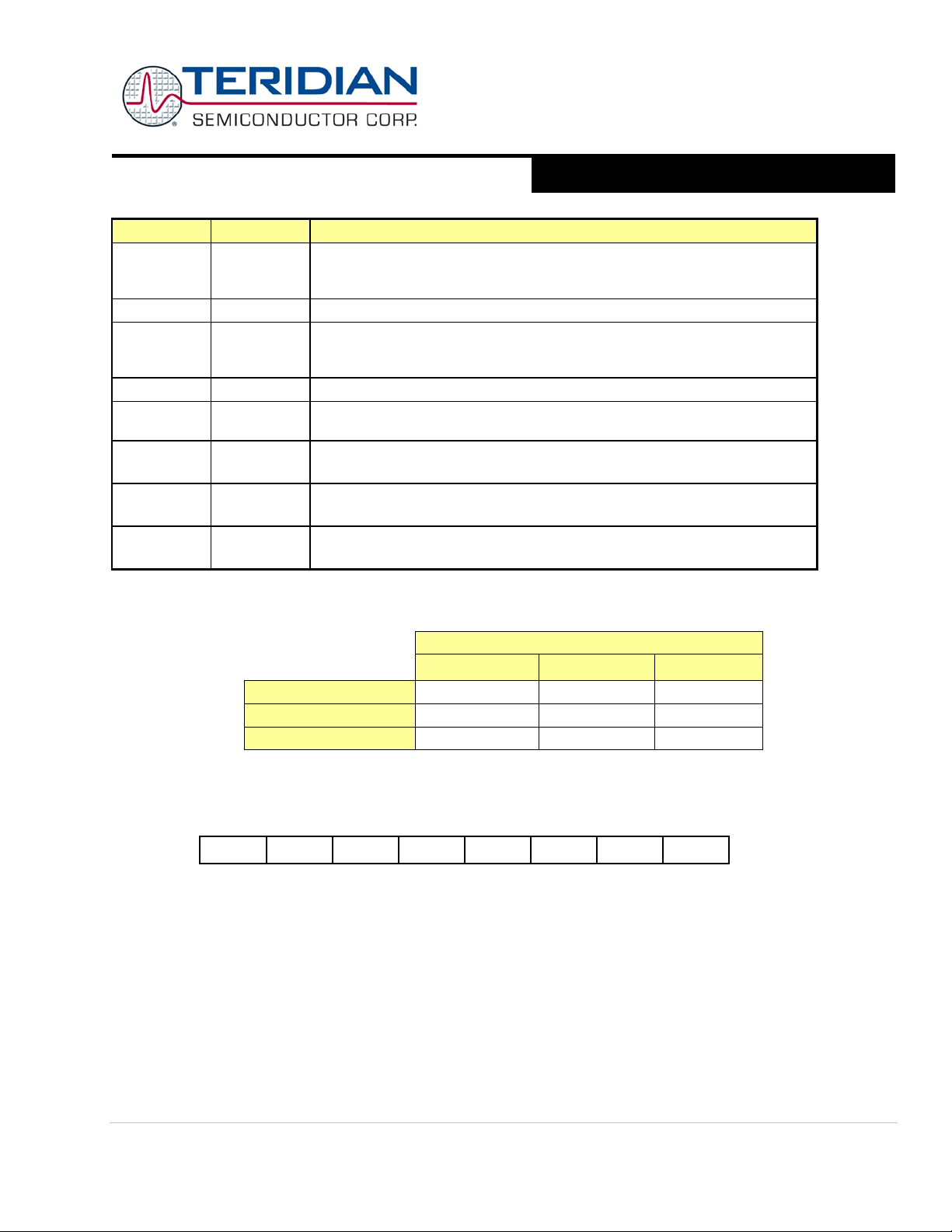
71M6513/71M6513H
3-Phase Energy Meter IC
DATA SHEET
A Maxim Integrated Products Brand
Bit
Symbol
Function
flag set by hardware when Timer 0 overflows. This flag can be
Interrupt 1 type control bit. Selects either the falling edge or low level on input
Interrupt 0 edge flag is set by hardware when the falling edge on external pin
Interrupt 0 type control bit. Selects either the falling edge or low level on input
Timer 0 - mode 0
YES
YES
YES
Timer 0 - mode 2
SMOD
The Timer 1 overflow flag is set by hardware when Timer 1 overflows. This flag
TCON.7 TF1
TCON.6 TR1 Tim er 1 Run control bit. If cleared, Timer 1 stops.
TCON.5 TF0
TCON.4 TR0 Tim er 0 Run control bit. If cleared, Timer 0 stops.
TCON.3 IE1
can be cleared by s oftware and is automati cally cleared when an interrupt is
processed.
Timer 0 overflow
cl eared b y software an d is automaticall y clear ed when a n interrupt is
processed.
Interrupt 1 edge flag is set by hardware when the falling edge on external pin
int1 is observed. Cleared when an interrupt is processed.
AUGUST 2011
TCON.2 IT1
TCON.1 IE0
TCON.0 IT0
Table 23 specifies the combinations of operation modes allowed for ti mer 0 and tim er 1:
Timer 0 - mode 1 YES YES YES
Timer/Counter Mode Control Register ( PCON):
MSB LSB
The SMOD bit in the PCON register doubles the b aud rate w hen set.
pin to cause an interrupt.
int0 is observed. Cleared when an interrupt is processed.
pin to cause interrupt.
Table 22: The TCON Register Bit Functions
Timer 1
Mode 0 Mode 1 Mode 2
Not allowed Not all o wed YES
Table 23: Timer Modes
Table 24: The PCON Register
WD Timer (Software Watchdog Timer)
The software watchdog timer is a 16-bit c ounter th at is in cremen ted onc e every 2 4 or 384 cl ock cy cles. Af ter a res et, th e
watchdog timer is disabled and all registers are set to zero. The watchdog consists of a 16-bit count er (WDT), a reload register
(WDTREL), prescalers (by 2 and by 16), and control logic. Once the watchdog is started, it cannot be stopped unless the
internal reset signal becomes active.
Note: It is recommended to use the hardware watchdog timer instead of the software watchdog timer.
WD Timer Start Procedure: The WD T is start ed b y settin g t h e SWDT flag. When t he WDT reg is ter ent er s th e st at e 0x7C FF ,
an asynchronous WDTS signal will become active. The signal WDTS sets bit 6 in the IP0 register and requests a reset state.
WDTS is cleared either by the reset si gnal or by chan ging the stat e of the WDT.
Page: 28 of 104 © 2005-2011 Teridian Semiconductor Corporation
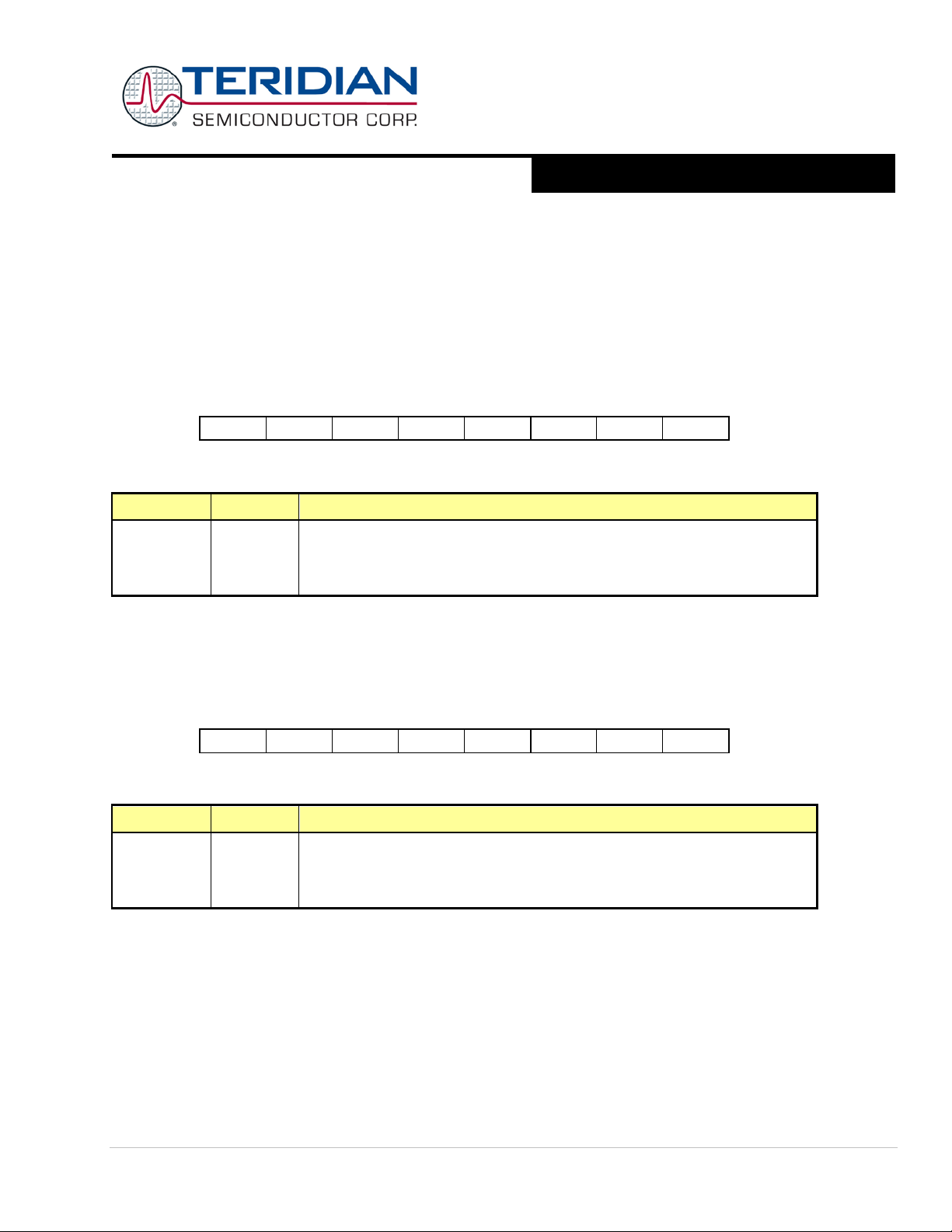
71M6513/71M6513H
3-Phase Energy Meter IC
DATA SHEET
A Maxim Integrated Products Brand
Bit
Symbol
Function
Bit
Symbol
Function
SEPTEMBER 2011
Refreshing the WD Timer: The watchdog timer must be refreshed regularly to prevent the reset request signal from
becoming active. This requirement imposes an obligation on the programmer to issue two instructions. The first instruction
sets WDT and t he second instruction sets SWDT. The maximum delay allowed between setting WDT and SWDT is 12 clock
cycles. If this period has expired and SWDT has not been set, WDT is automatically reset, otherwise the watchdog timer is
reloaded with the content of the WDTREL register and WDT is automatically reset. Since the W DT requires exact t iming,
firmware needs to be designed with special care in order to avoid unwanted WDT resets. Teridian strongly discourages the
use of the software WDT.
Special Function Registers for the WD Timer
Interrupt Enable 0 Register (IEN0):
MSB LSB
EAL WDT ET2 ES0 ET1 EX1 ET0 EX0
Table 25: The IEN0 Register (see also Table 32)
IEN0.6 WDT Watchdog timer refresh flag.
Set to initiat e a refr esh of the watc hdog timer. Must be set direc tly before SWDT is
set to prevent an unintentional r efresh of the w atchdog timer. WDT is reset by
hardware 12 clock cycles after it has been set.
Table 26: The IEN0 Bit Functions (see also Table 32)
Note: The remaining bits in the IEN0 register are not used for watchdog control
Interrupt Enable 1 Register (IEN1):
MSB LSB
EXEN2 SWDT EX6 EX5 EX4 EX3 EX2
Table 27: The IEN1 Register (see also Tables 30/31)
IEN1.6 SWDT Watchdo g t i mer start/ refr esh flag.
Set to acti vate/refresh th e watc hdog timer. When directl y set after setting WDT, a
watchdog timer refresh is performed. Bit SWDT is reset by the hardware 12 clock
cycles after it has been set.
Table 28: The IEN1 Bit Functions (see also Tables 30/31)
Note: The remaining bits in the IEN1 register are not used for watchdog control
© 2005-2011 Teridian Semiconductor Corporation Page: 29 of 104
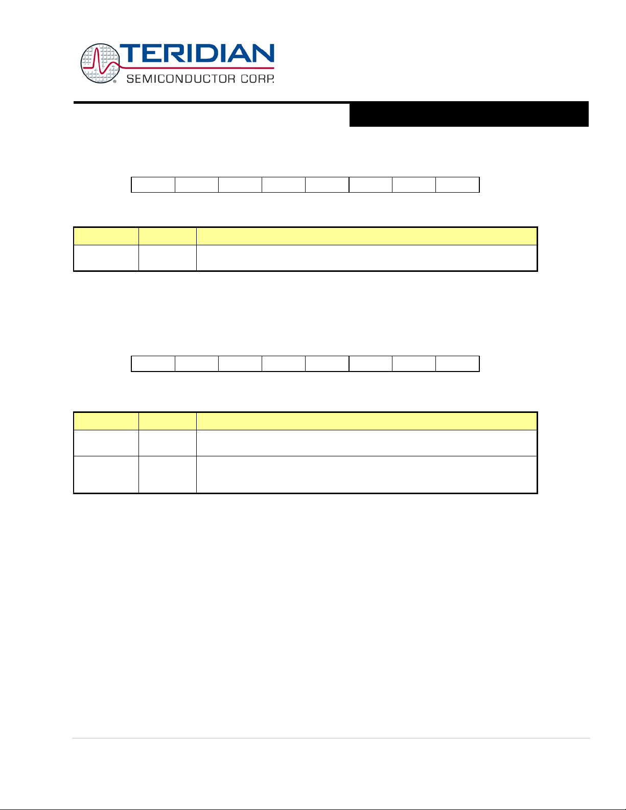
3-Phase Energy Meter IC
DATA SHEET
A Maxim Integrated Products Brand
Bit
Symbol
Function
IP0.6
WDTS
Watchdog timer status flag. Set when the watchdog timer was started. Can be
Bit
Symbol
Function
Interrupt Priority 0 Register (IP0):
MSB LSB
-- WDTS IP0.5 IP0.4 IP0.3 IP0.2 IP0.1 IP0.0
Table 29: The IP0 Register (see also Table 45)
read by softwar e.
Table 30: The IP0 bit Functions (see also Table 45)
Note: The remaining bits in the IP0 register are not used for watchdog control
Watchdog Timer Reload Register (WDTREL):
MSB LSB
7 6 5 4 3 2 1 0
71M6513/71M6513H
AUGUST 2011
Table 31: The WDTREL Register
WDTREL.7 7
WDTREL.6
to
WDTREL.0
The WDTREL register can be loaded and read at any time.
6-0
Prescaler select bit. When set, the watchdog is clocked through an additional
divide-by-16 prescaler
Seven bit reload value for t he high -b yte of the watchdog t imer. This value is
loaded to the WDT when a refresh is triggered by a consecutive setting of bits
WDT and SWDT.
Table 32: The WDTREL Bit Functions
Page: 30 of 104 © 2005-2011 Teridian Semiconductor Corporation
 Loading...