

TERIDIAN Semiconductor 71M6513, 71M6513H User Manual
71M6513/71M6513H Demo Board
USER’S MANUAL
4/9/2007 10:06 AM
Revision 5.6
TERIDIAN Semiconductor Corporation
6440 Oak Canyon Rd.
Irvine, CA 92618-5201
Phone: (714) 508-8800 ▪ Fax: (714) 508-8878
http://www.teridian.com/
meter.support@teridian.com

71M6513/71M6513H Demo Board User’s Manual
TERIDIAN Semiconductor Corporation makes no warranty for the use of its products, other than expressly contained in the Company’s
warranty detailed in the TERIDIAN Semiconductor Corporation standard Terms and Conditions. The company assumes no responsibility
for any errors which may appear in this document, reserves the right to change devices or specifications detailed herein at any time
without notice and does not make any commitment to update the information contained herein.
Page: 2 of 112
© 2005-2006 TERIDIAN Semiconductor Corporation Revision 5.6

71M6513/71M6513H Demo Board User’s Manual
71M6513/71M6513H
3-Phase Energy Meter IC
DEMO BOARD
USER’S MANUAL
Page: 3 of 112
© 2005-2006 TERIDIAN Semiconductor Corporation Revision 5.6

71M6513/71M6513H Demo Board User’s Manual
Table of Contents
1 GETTING STARTED.............................................................................................................................................. 9
1.1 General .................................................................................................................................................................. 9
1.2 Safety and ESD Notes.......................................................................................................................................... 9
1.3 Demo Kit Contents ............................................................................................................................................. 10
1.4 Demo Board Versions........................................................................................................................................ 10
1.5 Compatibility....................................................................................................................................................... 10
1.6 Suggested Equipment not Included ................................................................................................................. 10
1.7 Demo Board Test Setup..................................................................................................................................... 11
1.7.1 Power Supply Setup...................................................................................................................................... 14
1.7.2 Cable for Serial Connection (Debug Board) .................................................................................................. 14
1.7.3 Checking Operation....................................................................................................................................... 14
1.7.4 Serial Connection Setup................................................................................................................................ 15
1.8 Using the Demo Board....................................................................................................................................... 16
1.8.1 Serial Command Language........................................................................................................................... 17
1.8.2 Using the Demo Board for Energy Measurements ........................................................................................ 26
1.8.3 Adjusting the Kh Factor for the Demo Board................................................................................................. 26
1.8.4 Adjusting the Demo Boards to Different Current Transformers .....................................................................27
1.8.5 Adjusting the Demo Boards to Different Voltage Dividers ............................................................................. 27
1.9 Calibration Parameters ...................................................................................................................................... 28
1.9.1 General Calibration Procedure ...................................................................................................................... 28
1.9.2 Calibration Macro File ................................................................................................................................... 29
1.9.3 Updating the 6513_demo.hex file.................................................................................................................. 29
1.9.4 Updating Calibration Data in Flash Memory without Using the ICE or a Programmer................................... 29
1.9.5 Automatic Gains Calibration.......................................................................................................................... 30
1.9.6 Loading the 6513_demo.hex file into the Demo Board.................................................................................. 30
1.9.7 The Programming Interface of the 71M6513/6513H ..................................................................................... 32
1.10 Demo Code...................................................................................................................................................... 33
1.10.1 Demo Code Description............................................................................................................................. 33
1.10.2 Demo Code MPU Parameters ................................................................................................................... 34
1.10.3 Useful CLI Commands Involving the MPU and CE....................................................................................40
1.10.4 Demo Code for Neutral Detection (Demo Board D6513T3C1) .................................................................. 40
2 APPLICATION INFORMATION ........................................................................................................................... 43
2.1 Calibration Theory.............................................................................................................................................. 43
2.1.1 Calibration with Three Measurements........................................................................................................... 43
2.1.2 Calibration with Five Measurements.............................................................................................................. 45
2.2 Calibration Procedures...................................................................................................................................... 46
2.2.1 Calibration Procedure with Three Measurements ......................................................................................... 47
2.2.2 Calibration Procedure with Five Measurements ............................................................................................ 48
2.2.3 Calibration Procedure for Rogowski Coil Sensors......................................................................................... 48
2.2.4 Calibration Spreadsheets .............................................................................................................................. 49
2.2.5 Compensating for Non-Linearities ................................................................................................................. 53
Page: 4 of 112
© 2005-2006 TERIDIAN Semiconductor Corporation Revision 5.6

71M6513/71M6513H Demo Board User’s Manual
Power Saving Measures .................................................................................................................................... 54
2.3
2.4 Schematic Information....................................................................................................................................... 55
2.4.1 Components for the V1 Pin ........................................................................................................................... 55
2.4.2 Reset Circuit.................................................................................................................................................. 55
2.4.3 Oscillator ....................................................................................................................................................... 56
2.4.4 EEPROM....................................................................................................................................................... 56
2.4.5 LCD............................................................................................................................................................... 57
2.4.6 Optical Interface ............................................................................................................................................ 58
2.4.7 Connecting the RX Pin .................................................................................................................................. 59
2.4.8 Connecting the V3 Pin................................................................................................................................... 60
2.5 Testing the Demo Board .................................................................................................................................... 61
2.5.1 Functional Meter Test.................................................................................................................................... 61
2.5.2 EEPROM....................................................................................................................................................... 62
2.5.3 RTC............................................................................................................................................................... 63
2.5.4 Hardware Watchdog Timer............................................................................................................................ 63
2.5.5 LCD............................................................................................................................................................... 63
2.6 TERIDIAN Application Notes ............................................................................................................................. 64
3 HARDWARE DESCRIPTION............................................................................................................................... 65
3.1 D6513T3B2 Board Description: Jumpers, Switches and Test Points............................................................ 65
3.2 D6513T3C1 Board Description: Jumpers, Switches and Test Points............................................................ 69
3.3 D6513T3D2 Board Description: Jumpers, Switches and Test Points............................................................ 72
3.4 Board Hardware Specifications (D6513T3B2, D6513T3C1)............................................................................. 75
3.5 Board Hardware Specifications (D6513T3D2).................................................................................................. 76
4 APPENDIX ........................................................................................................................................................... 77
List of Figures
Figure 1-1: TERIDIAN D6513T3B2 Demo Board with Debug Board: Basic Connections ................................................. 11
Figure 1-2: Block diagram for the TERIDIAN D6513T3B2 Demonstration Meter with Debug Board................................. 12
Figure 1-3: Block diagram for the TERIDIAN D6513T3C1 and D6513T3D2 Demo Boards with Debug Board................. 13
Figure 1-4: Hyperterminal Sample Window with Disconnect Button (Arrow) ..................................................................... 15
Figure 1-5: Port Speed and Handshake Setup (left) and Port Bit setup (right).................................................................. 16
Figure 1-6: Command Line Help Display........................................................................................................................... 17
Figure 1-7: Typical Calibration Macro file .......................................................................................................................... 29
Figure 1-8: Emulator Window Showing Reset and Erase Buttons (see Arrows) ............................................................... 31
Figure 1-9: Emulator Window Showing Erased Flash Memory and File Load Menu......................................................... 31
Figure 2-1: Watt Meter with Gain and Phase Errors.......................................................................................................... 43
Figure 2-2: Phase Angle Definitions.................................................................................................................................. 47
Figure 2-3: Calibration Spreadsheet for Three Measurements ......................................................................................... 51
Figure 2-4: Calibration Spreadsheet for Five Measurements ............................................................................................ 51
Figure 2-5: Calibration Spreadsheet for Rogowski coil...................................................................................................... 52
Figure 2-6: Non-Linearity Caused by Quantification Noise................................................................................................ 53
Figure 2-7: Voltage Divider for V1 ..................................................................................................................................... 55
Figure 2-8: External Components for RESETZ ................................................................................................................. 55
Page: 5 of 112
© 2005-2006 TERIDIAN Semiconductor Corporation Revision 5.6

71M6513/71M6513H Demo Board User’s Manual
Figure 2-9: Oscillator Circuit.............................................................................................................................................. 56
Figure 2-10: EEPROM Circuit ........................................................................................................................................... 56
Figure 2-11: LCD Connections.......................................................................................................................................... 57
Figure 2-12: LCD Boost and LCD Control Registers......................................................................................................... 57
Figure 2-13: Optical Interface Block Diagram.................................................................................................................... 58
Figure 2-14: Optical Port Circuitry on the D6513T3B2 Demo Board ................................................................................. 58
Figure 2-15: Optical Port Circuitry on the D6513T3C1 Demo Board................................................................................. 59
Figure 2-16: Internal Diode Clamp on the RX Pin ............................................................................................................. 59
Figure 2-17: Resistor Network for RX................................................................................................................................ 60
Figure 2-18: Meter with Calibration System ...................................................................................................................... 61
Figure 2-19: Calibration System Screen............................................................................................................................ 62
Figure 3-1: D6513T3B2 Demo Board - Board Description (Default jumper settings indicated in yellow)........................... 68
Figure 3-2: D6513T3C1 Demo Board - Board Description ................................................................................................ 71
Figure 3-3: D6513T3D2 Demo Board - Board Description ................................................................................................ 74
Figure 4-1: TERIDIAN D6513T3B2 Demo Board: Electrical Schematic 1/3 ...................................................................... 78
Figure 4-2: TERIDIAN D6513T3B2 Demo Board: Electrical Schematic 2/3 ...................................................................... 79
Figure 4-3: TERIDIAN D6513T3B2 Demo Board: Electrical Schematic 2/3 ...................................................................... 80
Figure 4-4: TERIDIAN D6513T3C1 Demo Board: Electrical Schematic 1/3...................................................................... 81
Figure 4-5: TERIDIAN D6513T3C1 Demo Board: Electrical Schematic 2/3...................................................................... 82
Figure 4-6: TERIDIAN D6513T3C1 Demo Board: Electrical Schematic 3/3...................................................................... 83
Figure 4-7: TERIDIAN D6513T3D2 Demo Board: Electrical Schematic 1/3...................................................................... 84
Figure 4-8: TERIDIAN D6513T3D2 Demo Board: Electrical Schematic 2/3...................................................................... 85
Figure 4-9: TERIDIAN D6513T3D2 Demo Board: Electrical Schematic 3/3...................................................................... 86
Figure 4-10: TERIDIAN D6513T3B2 Demo Board: Top View ........................................................................................... 90
Figure 4-11: TERIDIAN D6513T3B2 Demo Board: Bottom View ...................................................................................... 91
Figure 4-12: TERIDIAN D6513T3B2 Demo Board: Top Signal Layer ............................................................................... 92
Figure 4-13: TERIDIAN D6513T3B2 Demo Board: Middle Layer 1 (Ground Plane) ......................................................... 93
Figure 4-14: TERIDIAN D6513T3B2 Demo Board: Middle Layer 2 (Supply Plane) .......................................................... 94
Figure 4-15: TERIDIAN D6513T3B2 Demo Board: Bottom Signal Layer .......................................................................... 95
Figure 4-16: TERIDIAN D6513T3C1 Demo Board: Top View ........................................................................................... 96
Figure 4-17: TERIDIAN D6513T3C1 Demo Board: Bottom View...................................................................................... 97
Figure 4-18: TERIDIAN D6513T3C1 Demo Board: Top Signal Layer ............................................................................... 98
Figure 4-19: TERIDIAN D6513T3C1 Demo Board: Ground Plane Layer .......................................................................... 99
Figure 4-20: TERIDIAN D6513T3C1 Demo Board: Power Plane Layer.......................................................................... 100
Figure 4-21: TERIDIAN D6513T3C1 Demo Board: Bottom Signal Layer........................................................................ 101
Figure 4-22: TERIDIAN D6513T3D2 Demo Board: Top Signal Layer ............................................................................. 102
Figure 4-23: TERIDIAN D6513T3D2 Demo Board: Bottom Signal Layer........................................................................ 103
Figure 4-24: TERIDIAN D6513T3D2 Demo Board: Bottom View.................................................................................... 104
Page: 6 of 112
© 2005-2006 TERIDIAN Semiconductor Corporation Revision 5.6

71M6513/71M6513H Demo Board User’s Manual
Figure 4-25: Debug Board: Electrical Schematic............................................................................................................. 106
Figure 4-26: Debug Board: Top View.............................................................................................................................. 107
Figure 4-27: Debug Board: Bottom View......................................................................................................................... 107
Figure 4-28: Debug Board: Top Signal Layer.................................................................................................................. 108
Figure 4-29: Debug Board: Middle Layer 1 (Ground Plane) ............................................................................................ 108
Figure 4-30: Debug Board: Middle Layer 2 (Supply Plane) ............................................................................................. 109
Figure 4-31: Debug Board: Bottom Trace Layer ............................................................................................................. 109
Figure 4-32: TERIDIAN 71M6513/71M6513H epLQFP100: Pinout (top view) ................................................................ 112
List of Tables
Table 1-1: Jumper settings on Debug Board..................................................................................................................... 14
Table 1-2: Straight cable connections ............................................................................................................................... 14
Table 1-3: Null-modem cable connections ........................................................................................................................ 14
Table 1-4: CE RAM Locations for Calibration Constants................................................................................................... 28
Table 1-5: Flash Programming Interface Signals .............................................................................................................. 32
Table 1-6: MPU Input Parameters for Metering................................................................................................................. 35
Table 1-7: MPU Input Parameters for Temperature Compensation .................................................................................. 35
Table 1-8: MPU Parameters for Pulse Source Selection................................................................................................... 36
Table 1-9: Selectable Pulse Sources ................................................................................................................................ 36
Table 1-10: MPU Instantaneous Output Variables ............................................................................................................ 37
Table 1-11: MPU Status Word Bit Assignment.................................................................................................................. 38
Table 1-12: MPU Accumulation Output Variables ............................................................................................................. 39
Table 1-13: CLI Commands for MPU Data Memory.......................................................................................................... 40
Table 1-14: Neutral Current Accuracy at Various Sampling Frequencies ......................................................................... 41
Table 2-1: Power Saving Measures .................................................................................................................................. 54
Table 3-1: D6513T3B2 Demo Board Description .............................................................................................................. 65
Table 3-2: D6513T3B2 Demo Board Description .............................................................................................................. 66
Table 3-3: D6513T3B2 Demo Board Description .............................................................................................................. 67
Table 3-4: D6513T3C1 Demo Board Description.............................................................................................................. 69
Table 3-5: D6513T3C1 Demo Board Description.............................................................................................................. 70
Table 3-6: D6513T3D2 Demo Board Description.............................................................................................................. 73
Table 4-1: D6513T3C1 Demo Board: Bill of Material ........................................................................................................ 87
Table 4-2: D6513T3B2 Demo Board: Bill of Material ........................................................................................................ 88
Table 4-3: D6513T3D2 Demo Board: Bill of Material ........................................................................................................ 89
Table 4-4: Debug Board: Bill of Material.......................................................................................................................... 105
Table 4-5: 71M6513/71M6513H Pin Description Table 1/3............................................................................................. 110
Table 4-6: 71M6513/71M6513H Pin Description Table 2/3............................................................................................. 110
Table 4-7: 71M6513/71M6513H Pin Description Table 3/3............................................................................................. 111
Page: 7 of 112
© 2005-2006 TERIDIAN Semiconductor Corporation Revision 5.6

71M6513/71M6513H Demo Board User’s Manual
Page: 8 of 112
© 2005-2006 TERIDIAN Semiconductor Corporation Revision 5.6
71M6513/71M6513H Demo Board User’s Manual
1
1 GETTING STARTED
1.1 GENERAL
The TERIDIAN Semiconductor Corporation (TSC) 71M6513/71M6513H Demo Board is a demonstration board
for evaluating the 71M6513/71M6513H device for 3-phase electronic power metering applications. It incorporates a 71M6513 or 71M6513H integrated circuit, peripheral circuitry such as a serial EEPROM, emulator
port, and on board power supply as well as a companion Debug Board that allows a connection to a PC through
a RS232 port. The demo board allows the evaluation of the 71M6513 or 71M6513H energy meter chip for
measurement accuracy and overall system use.
The board is pre-programmed with a Demo Program (file name 6513_demo.hex) in the FLASH memory of the
71M6513/6513H IC. This embedded application is developed to exercise all low-level function calls to directly
manage the peripherals, flash programming, and CPU (clock, timing, power savings, etc.).
The 71M6513/6513H IC on the Demo Board is pre-programmed with default calibration factors.
1.2 SAFETY AND ESD NOTES
Connecting live voltages to the demo board system will result in potentially hazardous voltages on the demo
board.
BEFORE OPERATING THE DEMO BOARD, THE JUMPERS ON JP2 AND JP3 (IF IN-
STALLED) SHOULD BE REMOVED! IT IS RECOMMENDED TO OPERATE THE
DEBUG BOARD WITH ITS OWN POWER SUPPLY.
THE DEMO SYSTEM IS ESD SENSITIVE! ESD PRECAUTIONS SHOULD BE TAKEN
WHEN HANDLING THE DEMO BOARD!
EXTREME CAUTION SHOULD BE TAKEN WHEN HANDLING THE DEMO BOARD
ONCE IT IS CONNECTED TO LIVE VOLTAGES!
Page: 9 of 112
© 2005-2006 TERIDIAN Semiconductor Corporation Revision 5.6

71M6513/71M6513H Demo Board User’s Manual
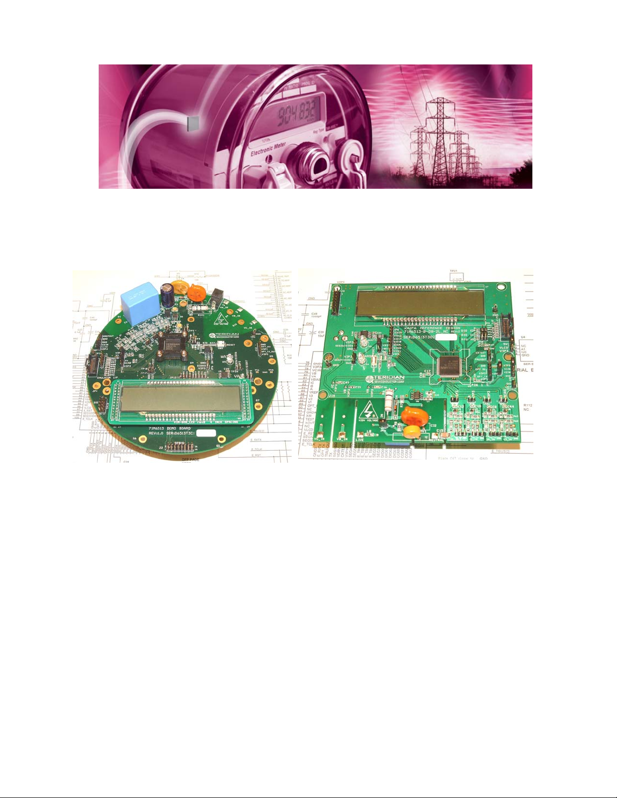
1.3 DEMO KIT CONTENTS
• Demo Board with 71M6513/71M6513H IC and pre-loaded demo program:
• D6513T3B2 Demo Board (standard poly-phase), or
• D6513T3C1 Demo Board (poly-phase w/ added neutral current capability)
• Debug Board
• Two 5VDC/1,000mA universal wall transformers with 2.5mm plug (Switchcraft 712A compatible)
• Serial cable, DB9, Male/Female, 2m length (Digi-Key AE1020-ND)
• CD-ROM containing documentation (data sheet, board schematics, BOM, layout), Demo Code (sources
and executable), and utilities
The CD-ROM contains a file named readme.txt that specifies all files found on the media and their
purpose.
1.4 DEMO BOARD VERSIONS
The following versions of the Demo Board are available:
• Demo Board D6513T3B2 (standard)
• Demo Board D6513T3C1 (with neutral current detection capability)
• Demo Board D6513T3D2 (two layer PCB, with neutral current detection capability)
1.5 COMPATIBILITY
This manual applies to the following hardware and software revisions:
• 71M6513 or 71M6513H chip revision B03
• Demo Kit firmware revision 3.04 and 3.05 or later
• Demo Boards D6513T3B2, D6513T3C1 and D6513T3D2
1.6 SUGGESTED EQUIPMENT NOT INCLUDED
For functional demonstration:
• PC w/ MS-Windows versions XP, ME, or 2000, equipped with RS232 port (COM port) via DB9 connector
For software development (MPU code):
• Signum ICE (In Circuit Emulator): ADM-51
http://www.signum.com
• Keil 8051 “C” Compiler kit: CA51
http://www.keil.com/c51/ca51kit.htm
, http://www.keil.com/product/sales.htm
Page: 10 of 112
© 2005-2006 TERIDIAN Semiconductor Corporation Revision 5.6
71M6513/71M6513H Demo Board User’s Manual
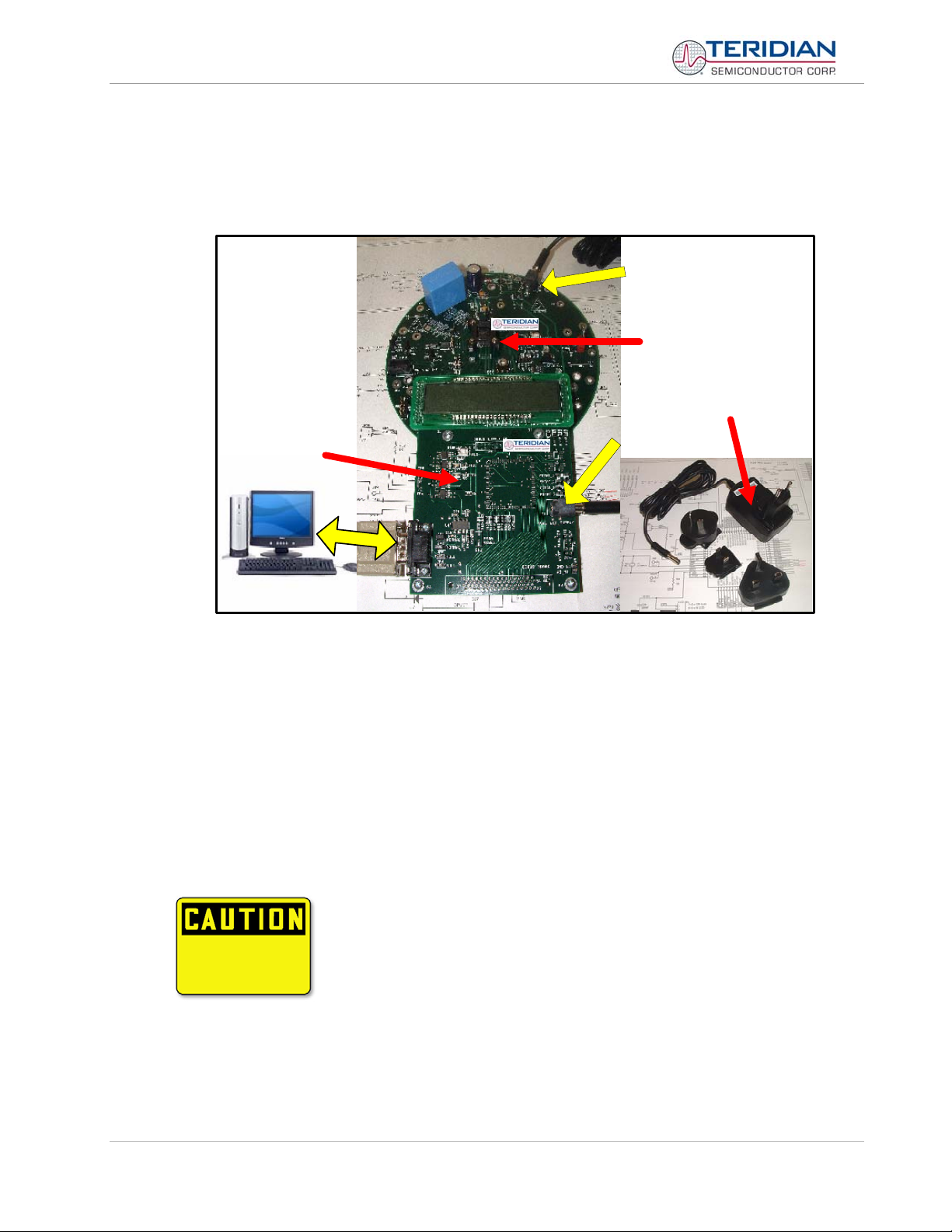
1.7 DEMO BOARD TEST SETUP
Figure 1-1 shows the basic connections of the Demo Board plus Debug Board with the external equipment for
desktop testing, i.e. without live power applied. For desktop testing, both the Demo and Debug board may be
powered with just the 5VDC power supplies.
Power
Demo Board
Power Supply
(100 to 240VAC,
1ADC Output)
Debug
Board
Power
Host PC
Figure 1-1: TERIDIAN D6513T3B2 Demo Board with Debug Board: Basic Connections
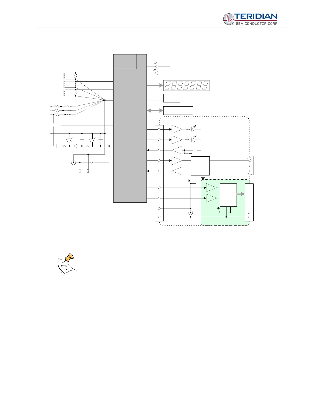
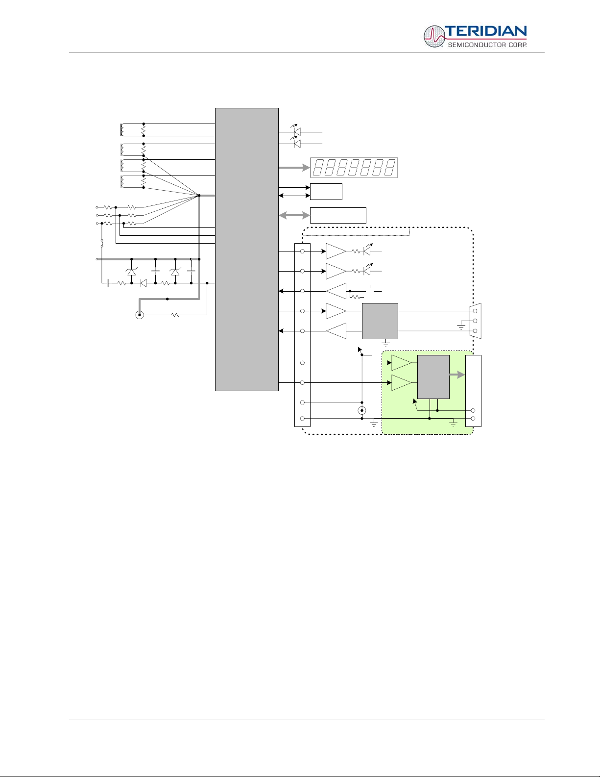
The D6513/T3B2 Demo Board block diagram is shown in Figure 1-2. It consists of a stand-alone (round) meter
Demo Board and an optional Debug Board. The Demo Board contains all circuits necessary for operation as a
meter, including display, calibration LED, and internal power supply. The Debug Board, when using a separate
power supply, is optically isolated from the meter and interfaces to a PC through a 9 pin serial port. For serial
communication between the PC and the TERIDIAN 71M6513/71M6513H, the Debug Board needs to be
plugged with its connector J3 into connector J2 of the Demo Board.
The D6513/T3C1 Demo Board System is shown in Figure 1-3. It is almost identical to the D6513T3B2, except
that the neutral current input is added and the optional power and ground connections from the Demo Board to
the Debug Board were removed.
Connections to the external signals to be measured, i.e. scaled AC voltages and current signals derived from
shunt resistors or current transformers, are provided on the rear side of the demo board.
Caution: It is recommended to set up the demo board with no live AC voltage
connected, and to connect live AC voltages only after the user is familiar with
the demo system.
Page: 11 of 112
© 2005-2006 TERIDIAN Semiconductor Corporation Revision 5.6
71M6513/71M6513H Demo Board User’s Manual
DEMONSTRATION METER
6513
External Current
Transformers
VC
VB
VA
JP1
NEUT
IA
IB
IC
5V
DC
V3P3
JP2 JP3
3.3v
GND
Single Chip
Meter
IA
IB
IC
V3P3
VA
VB
VC
GND
TMUXOUT
DIO6
DIO7
DIO4
DIO5
DIO0
DIO1
DIO2
RX
CKTEST
WATT
VAR
EEPROM
DEBUG BOARD (OPTIONAL)
TX
PULSE OUTPUTS
V3P3
V3P3
5V LCD DISPLAY
ICE Connector
OPTO
OPTO
CYCLE DISPLAY
OPTO
OPTO
OPTO
OPTO SUPPLY
V5_DBG
5V DC
GND_DBG
MPU HEARTBEAT (5Hz)
V5_DBG
CE HEARTBEAT (1Hz)
V5_DBG
GND_DBG
V5_DBG
RS-232
INTERFACE
OPTO
OPTO
OPTO SUPPLY
RTM INTERFACE
FPGA
V5_NI
DB9
to PC
COM Port
J5
68 Pin Connector
to NI PCI-6534
DIO Board
Figure 1-2: Block diagram for the TERIDIAN D6513T3B2 Demonstration Meter with Debug Board
Page: 12 of 112
All input signals are referenced to the V3P3 (3.3V power supply to the chip).
© 2005-2006 TERIDIAN Semiconductor Corporation Revision 5.6
71M6513/71M6513H Demo Board User’s Manual
DEMONSTRATION METER
External Current
Transformers
INEUTRAL
IA
IB
IC
VC
VB
VA
JP1
NEUT
5V
DC
V3P3
3.3v
GND
V3
VBIAS
IA
IB
Single Chip
IC
V3P3
VA
VB
VC
GND
DIO6
DIO7
6513
Meter
DIO4
DIO5
DIO0
DIO1
DIO2
TX
RX
PULSE OUTPUTS
WATT
V3P3
VAR
V3P3
5V LCD DISPLAY
EEPROM
ICE Connector
DEBUG BOARD (OPTIONAL)
OPTO
OPTO
OPTO
OPTO
OPTO
OPTO SUPPLY
MPU HEARTBEAT (5Hz)
V5_DBG
CE HEARTBEAT (1Hz)
V5_DBG
CYCLE DISPLAY
GND_DBG
V5_DBG
RS-232
INTERFACE
DB9
to PC
COM Port
TMUXOUT
CKTEST
V5_DBG
GND_DBG
5V DC
OPTO
OPTO
OPTO SUPPLY
OPTIONAL
RTM INTERFACE
FPGA
(optional)
V5_NI
J5
68 Pin Connector
to NI PCI-6534
DIO Board
Figure 1-3: Block diagram for the TERIDIAN D6513T3C1 and D6513T3D2 Demo Boards with Debug Board
Page: 13 of 112
© 2005-2006 TERIDIAN Semiconductor Corporation Revision 5.6
71M6513/71M6513H Demo Board User’s Manual
1.7.1 POWER SUPPLY SETUP
There are several choices for meter power supply:
• Internal (using phase A of the AC line voltage). The internal power supply is only suitable when phase A
exceeds 220V RMS.
• External 5VDC connector (J1) on the Demo Board
• External 5VDC connector (J1) on the Debug Board.
The three power supply jumpers, JP1, JP2, and JP3 (JP2/JP3 is only provided on the D6513T3B2
Demo Board), must be consistent with the power supply choice. JP1 connects the AC line voltage to
the internal power supply. This jumper should usually be left in place. JP2 and JP3 should be left
open (unconnected).
1.7.2 CABLE FOR SERIAL CONNECTION (DEBUG BOARD)
For connection of the DB9 serial port to a PC, either a straight or a so-called “null-modem” cable may be used.
JP1 and JP2 are plugged in for the straight cable, and JP3/JP4 are empty. The jumper configuration is reversed
for the null-modem cable, as shown in Table 1-1.
Cable
Configuration
Straight Cable
Null-Modem Cable Alternative -- -- Installed Installed
JP1 through JP4 can also be used to alter the connection when the PC is not configured as a DCE device.
Table 1-2 shows the connections necessary for the straight DB9 cable and the pin definitions.
Table 1-3 shows the connections necessary for the null-modem DB9 cable and the pin definitions.
Mode
Default
Table 1-1: Jumper settings on Debug Board
PC Pin Function Demo Board Pin
2 TX 2
3 RX 3
5 Signal Ground 5
Table 1-2: Straight cable connections
PC Pin Function Demo Board Pin
2 TX 3
3 RX 2
5 Signal Ground 5
JP1 JP2 JP3 JP4
Installed Installed -- --
Jumpers on Debug Board
Table 1-3: Null-modem cable connections
1.7.3 CHECKING OPERATION
A few seconds after power up, the LCD display on the Demo Board should display this brief greeting:
H E L L 0
Page: 14 of 112
© 2005-2006 TERIDIAN Semiconductor Corporation Revision 5.6
71M6513/71M6513H Demo Board User’s Manual
The “HELLO” message should be followed by the display of accumulated energy:
3. 0. 0 0 1
The decimal dot in the leftmost segment will be blinking, indicating activity of the MPU inside the
71M6513/6513H.
If contacts 3 and 5 of J2 are shorted with a jumper (or if the “DISPLAY SEL” switch SW2 on the Debug Board is
pressed and held down), the display will show a series of incrementing numbers (1 through 12) in the leftmost
digit(s) followed by the default date (2001.01.01) at number 10.
Once, the Debug Board is plugged into J2 of the Demo Board, LED DIO1 on the Debug Board will flash with a
frequency of 1Hz, indicating CE activity. The LED DIO0 will flash with a frequency of 5Hz, indicating MPU
activity.
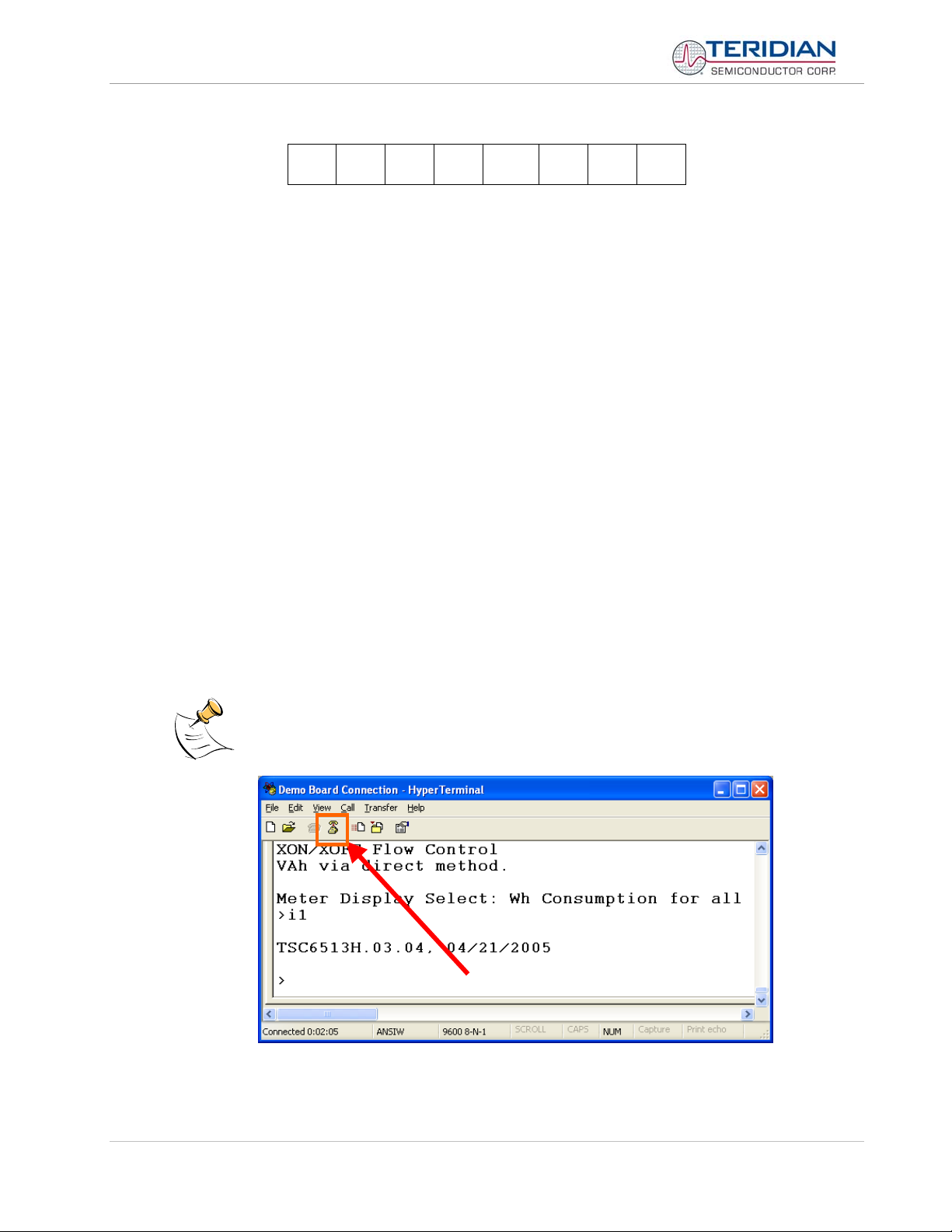
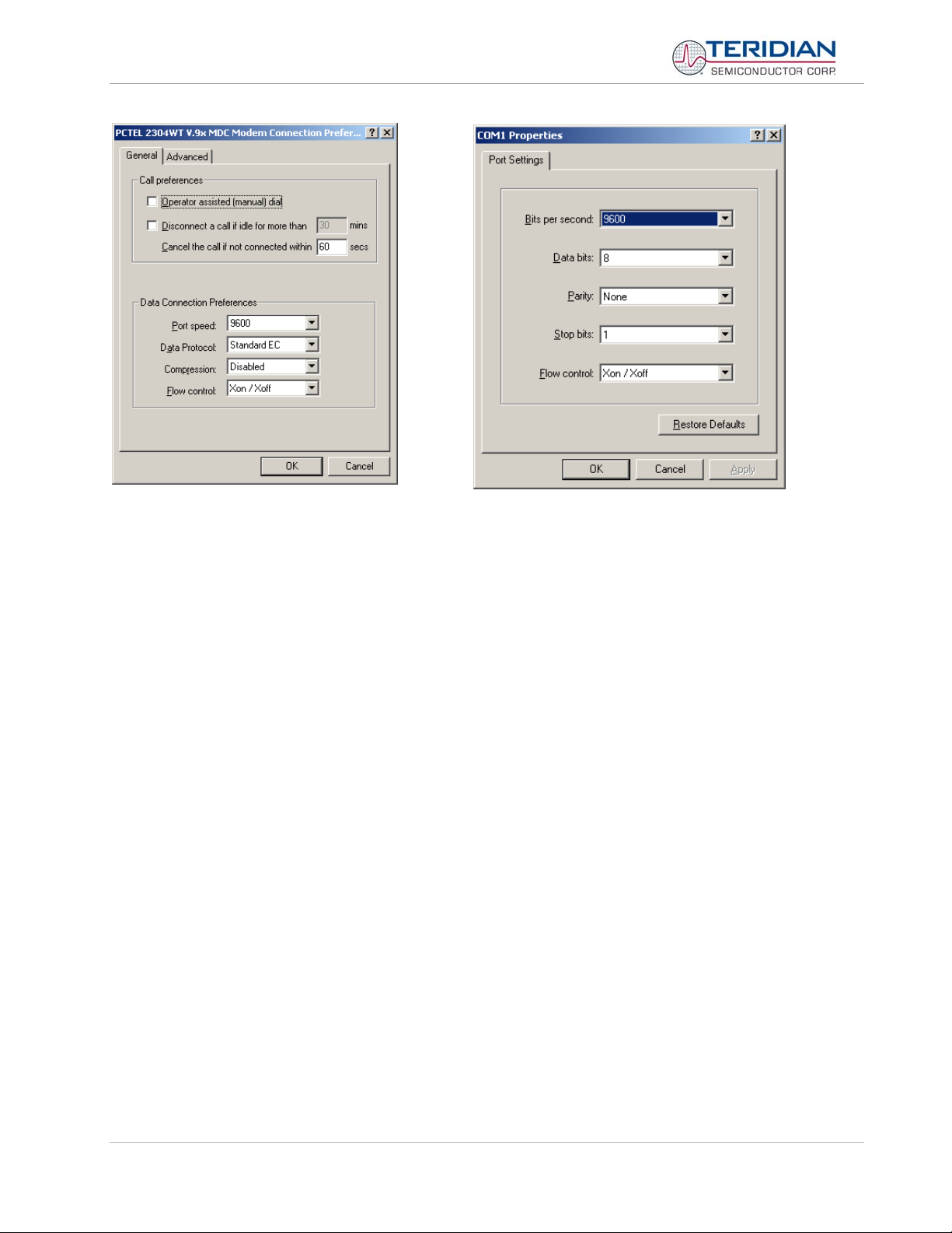
1.7.4 SERIAL CONNECTION SETUP
After connecting the DB9 serial port to a PC, start the HyperTerminal application and create a session using the
following parameters:
Port Speed: 9600 baud
Data Bits: 8
Parity: None
Stop Bits: 1
Flow Control: XON/XOFF
HyperTerminal can be found by selecting Programs ÆAccessories Æ Communications from the Windows
menu. The connection parameters are configured by selecting File Æ Properties and then by pressing the
Configure button. Port speed and flow control are configured under the General tab (Figure 1-5, left), bit settings
are configured by pressing the Configure button (Figure 1-6, right), as shown below. A setup file (file name
“Demo Board Connection.ht”) for HyperTerminal that can be loaded with File Æ Open is also provided with the
tools and utilities.
start
Port parameters can only be adjusted when the connection is not active. The disconnect
Page: 15 of 112
button, as shown in Figure 1-4 must be clicked in order to disconnect the port.
Figure 1-4: Hyperterminal Sample Window with Disconnect Button (Arrow)
© 2005-2006 TERIDIAN Semiconductor Corporation Revision 5.6
71M6513/71M6513H Demo Board User’s Manual
Figure 1-5: Port Speed and Handshake Setup (left) and Port Bit setup (right)
Once, the connection to the demo board is established, press <CR> and the prompt, >, should appear. Type
>? to see the Demo Code help menu. Type >i1 to verify that the demo code revision is 3.04 or later.
1.8 USING THE DEMO BOARD
The 71M6513/6513H Demo Board is a ready-to-use meter prepared for use with an external current transformer.
Using the Demo Board involves communicating with the Demo Code via the command line interface (CLI). The
CLI allows all sorts of manipulations to the metering parameters, access to the EEPROM, initiation of auto-cal
sequences, selection of the displayed parameters, changing calibration factors and many more operations.
Before evaluating the 71M6513/6513H on the Demo Board, users should get familiar with the commands and
responses of the CLI. A complete description of the CLI is provided in section 1.8.1.
Page: 16 of 112
© 2005-2006 TERIDIAN Semiconductor Corporation Revision 5.6
71M6513/71M6513H Demo Board User’s Manual
1.8.1 SERIAL COMMAND LANGUAGE
The Demo Code residing in the flash memory of the 71M6513/6513H provides a convenient way of examining
and modifying key meter parameters. Once the Demo Board is connected to a PC or terminal per the
instructions given in Section 1.7.2 and 1.7.4, typing ‘
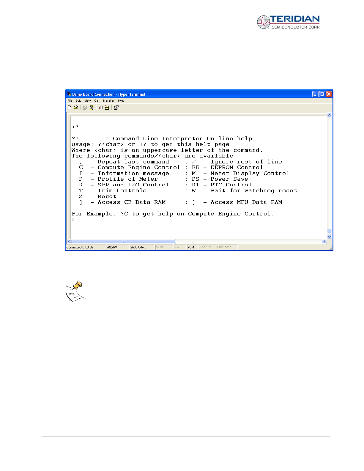
?’ will bring up the list of commands shown in Figure 1-6.
Figure 1-6: Command Line Help Display
The tables in this chapter describe the commands in detail.
Demo Code revision 3.05 offers more commands than revision 3.04. Commands only
available on 3.05 are marked in the tables presented in this chapter.
Page: 17 of 112
© 2005-2006 TERIDIAN Semiconductor Corporation Revision 5.6
71M6513/71M6513H Demo Board User’s Manual
Commands to Display Help on the CLI Commands:
? HELP
Description:
Command
combinations:
?] Display help on access CE data RAM
?) Display help on access MPU RAM
?, Display help on repeat last command
?/ Display help on ignore rest of line
?C
?EE Display help on EEPROM control
?I Display help on information message
?M Display help on meter display control
?P Display help on profile of meter
?R Display help on SFR control
?RT Display help on RTC control
?T Display help on trim control
?Z Display help on reset
Examples:
?C Displays compute engine control help.
Command help available for each of the options below.
? Command line interpreter help menu.
Display help on compute engine control and calibration.
In 3.05, pulse counter functions are offered.
?W Display help on the wait/reset command – 3.05 only
?? Display the command line interpreter help menu.
Commands for CE Data Access:
] CE DATA ACCESS
Description:
Usage:
Command
combinations:
Example:
]7E=12345678=9876ABCD Writes two words starting @ 0x7E
Allows user to read from and write to CE data space.
] [Starting CE Data Address] [option]…[option]
]A??? Read consecutive 16-bit words in Decimal, starting at
address A
]A$$$ Read consecutive 16-bit words in Hex, starting at address A
]A=n=n Write consecutive memory values, starting at address A
]U Update default version of CE Data in flash memory
]40$$$ Reads CE data words 0x40, 0x41 and 0x42.
CE data space is the address range for the CE DRAM (0x1000 to 0x13FF). All CE data words are in 4-byte (32bit) format. The offset of 0x1000 does not have to be entered when using the ] command, thus typing ]A? will
access the 32-bit word located at the byte address 0x1000 + 4 * A = 0x1028.
Page: 18 of 112
© 2005-2006 TERIDIAN Semiconductor Corporation Revision 5.6
71M6513/71M6513H Demo Board User’s Manual
Commands for MPU/XDATA Access:
) MPU DATA ACCESS
Description:
Usage:
Command
combinations:
Example:
)04=12345678=9876ABCD Writes two words starting @ 0x04
Allows user to read from and write to MPU data space.
) [Starting MPU Data Address] [option]…[option]
)A??? Read three consecutive 32-bit words in Decimal, starting at
address A
)A$$$ Read three consecutive 32-bit words in Hex, starting at
address A
)A=n=m Write the values n and m to two consecutive addresses
starting at address A
)08$$$$ Reads data words 0x08, 0x0C, 0x10, 0x14
MPU or XDATA space is the address range for the MPU XRAM (0x0000 to 0x3FF). All MPU data words are in
4-byte (32-bit) format. Typing ]A? will access the 32-bit word located at the byte address 4 * A = 0x28. The
energy accumulation registers of the Demo Code can be accessed by typing two Dollar signs (“$$”), typing
question marks will display negative decimal values if the most significant bit is set.
RAM access is limited to the lower 1KB address range. Read and write operations will “wrap around”
at higher addresses, i.e. )200? will yield the same result as )0?
Commands for DIO RAM (Configuration RAM) and SFR Control:
R DIO AND SFR CONTROL
Description:
Usage:
Command
combinations:
Example:
Allows the user to read from and write to DIO RAM and special function registers (SFRs).
R [option] [register] … [option]
RIx… Select I/O RAM location x (0x2000 offset is automatically
added)
Rx… Select internal SFR at address x
Ra???... Read consecutive SFR registers in Decimal, starting at
address a
Ra$$$... Read consecutive registers in Hex, starting at address a
Ra=n=m… Set values of consecutive registers to n and m starting at
address a
RI2$$$ Read DIO RAM registers 2, 3, and 4 in Hex.
DIO or Configuration RAM space is the address range 0x2000 to 0x20FF. This RAM contains registers used for
configuring basic hardware and functional properties of the 71M6513/6513H and is organized in bytes (8 bits).
The
0x2000 offset is automatically added when the command RI is typed.
The SFRs (special function registers) are located in internal RAM of the 80515 core, starting at address 0x80.
Page: 19 of 112
© 2005-2006 TERIDIAN Semiconductor Corporation Revision 5.6
71M6513/71M6513H Demo Board User’s Manual
Commands for EEPROM Control:
EE EEPROM CONTROL
Description:
Usage:
Command
combinations:
Example:
Allows user to enable read and write to EEPROM.
EE [option] [arguments]
EECn EEPROM Access (1 Æ Enable, 0 Æ Disable)
EERa.b Read EEPROM at address 'a' for 'b' bytes.
EESabc..xyz Write characters to buffer (sets Write length)
EETa Transmit buffer to EEPROM at address 'a'.
EEWa.b...z Write values to buffer
EEShello
EET$0210
Writes 'hello' to buffer, then transmits buffer to EEPROM
starting at address 0x210.
Due to buffer size restrictions, the maximum number of bytes handled by the EEPROM command is
0x40.
Auxiliary Commands:
Typing a comma (“,”) repeats the command issued from the previous command line. This is very helpful when examining
the value at a certain address over time, such as the CE DRAM address for the temperature (0x40).
The slash (“/”) is useful to separate comments from commands when sending macro text files via the serial interface. All
characters in a line after the slash are ignored.
Commands controlling the CE, TMUX and the RTM:
C COMPUTE ENGINE
CONTROL
Description:
Usage:
Command
combinations:
Example:
Allows the user to enable and configure the compute engine.
C [option] [argument]
CEn Compute Engine Enable (1 Æ Enable,
0 Æ Disable)
CTn Select input n for TMUX output pin. n is interpreted as a
decimal number.
CREn RTM output control (1 Æ Enable, 0 Æ Disable)
CRSa.b.c.d Selects CE addresses for RTM output
CE0 Disables CE, followed by “CE OFF” display on LCD. The
Demo Code will reset if the WD timer is enabled.
CT3 Selects the VBIAS signal for the TMUX output pin
Page: 20 of 112
© 2005-2006 TERIDIAN Semiconductor Corporation Revision 5.6
71M6513/71M6513H Demo Board User’s Manual
Commands controlling the Auto-Calibration Function:
CL AUTO-CALIBRATION
CONTROL
Description:
Usage:
Command
combinations:
Example:
Allows the user to initiate auto-calibration and to store calibration values.
CL [option]
CLB Begin auto-calibration. Prior to auto-calibration, the calibration
CLS Save calibration coefficients to EEPROM starting at address
CLR Restore calibration coefficients from EEPROM
CLD Restore coefficients from flash memory
CLB Starts auto-calibration
Before starting the auto-calibration process, target values for voltage and current must be entered in I/O RAM
prior to calibration (V at 0x2029, I at 0x202A, duration in accumulation intervals at 0x2028), and the target voltage
and current must be applied constantly during calibration. No phase adjustment will be performed. Coefficients
can be saved to EEPROM using the CLS command.
coefficients are automatically restored from flash memory. If
the coefficients are not unity gain (0x4000), auto-calibration
will yield poor results.
0x0004
Commands controlling the Pulse Counter Function (Demo Code Revision 3.05 only)
CP PULSE-COUNT CONTROL
Description:
Usage:
Command
combinations:
Example:
Allows the user to control the pulse count functions.
CP [option]
CPA Start pulse counting for time period defined with the CPD
command. Pulse counts will display with commands M15.2,
M16.2
CPC Clear the absolute pulse count displays (shown with
commands M15.1, M16.1)
CPDn Set time window for pulse counters to n seconds, n is inter-
preted as a decimal number.
CPD60 Set time window to 60 seconds.
Page: 21 of 112
Pulse counts accumulated over a time window defined by the CPD command will be displayed by
M15.2 or M16.2 after
Commands M15.1 and M16.1 will display the absolute
the defined time has expired.
pulse count for the W and VAR outputs.
These displays are reset to zero with the CPC command (or the XRAM write )1=2).
Commands M15.2 and M16.2 will display the number of pulses counted during the interval defined
by the CPD command. These displays are reset only after a new reading, as initiated by the CPA
command.
© 2005-2006 TERIDIAN Semiconductor Corporation Revision 5.6
71M6513/71M6513H Demo Board User’s Manual
Commands for Identification and Information:
I INFORMATION MESSAGES
Description:
Usage:
Command
combinations:
Example:
The I commands are mainly used to identify the revisions of Demo Code and the contained CE code.
Allows user to read and write information messages.
I [option] [argument]
I0 Displays complete version information
I1 Displays Demo Code version string
I1=abcdef Change Demo Code version string
I2 Displays Copyright string
I3 CE Version string
I3=abcdef Change CE Code version string
I1 Returns Demo Code version
P PROFILE OF METER
Description:
Usage:
Returns current meter configuration
profile
P
The profile of the meter is a summary of the important settings of the I/O RAM registers.
Page: 22 of 112
© 2005-2006 TERIDIAN Semiconductor Corporation Revision 5.6
71M6513/71M6513H Demo Board User’s Manual
Commands for Controlling the Metering Values Shown on the LCD Display:
M METER DISPLAY
CONTROL (LCD)
Description:
Usage:
Command
combinations:
M2 Frequency (Hz)
M3. [phase] Wh Total Consumption (display wraps around at 999.999)
M4. [phase] Wh Total Inverse Consumption (display wraps around at 999.999)
M5. [phase] VARh Total Consumption (display wraps around at 999.999)
M6. [phase] VARh Total Inverse Consumption (display wraps around at 999.999)
M7. [phase] VAh Total (display wraps around at 999.999)
M8 Operating Time (in hours)
M9 Real Time Clock
M10 Calendar Date
M11. [phase] V/I Angle at Phase (degrees)
M13.1 Main edge count (accumulated) – zero transitions of the input signal
M13.2 CE main edge count for the last accumulation interval
M14.1
M14.2
M15.1
M15.2
Example:
Allows user to select internal variables to be displayed.
M [option]. [option]
M Displays “HELLO” message
M0 Disables display updates
M1 Temperature (C° delta from nominal)
Absolute count for W pulses. Reset with CPC command. Demo Code
revision 3.05 only.
Count for W pulses in time window defined by the CPD command. Demo
Code revision 3.05 only.
Absolute count for VAR pulses. Reset with CPC command. Demo Code
revision 3.05 only.
Count for W pulses in time window defined by the CPD command. Demo
Code revision 3.05 only.
M3.3 Displays Wh total consumption of phase C.
M5.0 Displays VARh total consumption for all phases.
Displays for total consumption wrap around at 999.999Wh (or VARh, VAh) due to the limited
Page: 23 of 112
number of available display digits. Internal registers (counters) of the Demo Code are 64 bits
wide and do not wrap around.
When entering the phase parameter, use 1 for phase A, 2 for phase B, 3 for phase C, and 0 for all
phases.
© 2005-2006 TERIDIAN Semiconductor Corporation Revision 5.6
71M6513/71M6513H Demo Board User’s Manual
Commands for Controlling the RMS Values Shown on the LCD Display:
MR METER RMS DISPLAY
CONTROL (LCD)
Description:
Usage:
Command
combinations:
MR2. [phase] Displays instantaneous RMS voltage
Example:
Allows user to select meter RMS display for voltage or current.
MR [option]. [option]
MR1. [phase] Displays instantaneous RMS current
MR1.3 Displays phase C RMS current.
On the D6513T3C1 Demo Boards, phase 4 is the measured neutral current.
No error message is issued when an invalid parameter is entered, e.g. MR1.8.
Commands for Controlling the MPU Power Save Mode:
PS POWER SAVE MODE
Description:
Usage:
Return to normal mode is achieved by resetting the MPU (Z command).
Enters power save mode Disables CE, ADC, CKOUT, ECK, RTM, SSI, TMUX VREF,
and serial port, sets MPU clock to 38.4KHz.
PS
Commands for Controlling the RTC:
RT REAL TIME CLOCK
CONTROL
Description:
Usage:
Command
combinations:
Example:
Allows the user to read and set the real time clock.
RT [option] [value] … [value]
RTDy.m.d.w: Day of week (year, month, day, weekday [1 = Sunday])
RTR Read Real Time Clock.
RTTh.m.s Time of day: (hr, min, sec).
RTAs.t Real Time Adjust: (start, trim). Allows trimming of the RTC.
RTD05.03.17.5 Programs the RTC to Thursday, 3/17/2005
RTA1.+1234 Speeds up the RTC by 1234 PPB.
The “Military Time Format” is used for the RTC, i.e. 15:00 is 3:00 PM.
If s > 0, the speed of the clock will be adjusted by ‘t’ parts per
billion (PPB). If the CE is on, the value entered with 't' will be
changing with temperature, based on Y_CAL, Y_CALC and
Y_CALC2.
Page: 24 of 112
© 2005-2006 TERIDIAN Semiconductor Corporation Revision 5.6
71M6513/71M6513H Demo Board User’s Manual
Commands for Accessing the Trim Control Registers:
T TRIM CONTROL
Description:
Usage:
Command
combinations:
Example:
Allows user to read trim and fuse values.
T [option]
T4 Read fuse 4 (TRIMM).
T5 Read fuse 5 (TRIMBGA)
T6 Read fuse 6 (TRIMBGB).
T4 Reads the TRIMM fuse.
These commands are only accessible for the 71M6513H (0.1%) parts. When used on a 71M6513 (0.5%) part,
the results will be displayed as zero.
Reset Commands:
W, Z RESET
Description:
Usage:
Commands:
Soft Reset and watchdog control
W, Z
W Halts the Demo Code program, thus suppressing the trigger-
ing of the hardware watchdog timer. This will cause a reset, if
the watchdog timer is enabled.
Demo Code revision 3.05 only.
Z Soft reset. This command acts like a hardware reset. The
energy accumulators in XRAM will retain their values.
Page: 25 of 112
© 2005-2006 TERIDIAN Semiconductor Corporation Revision 5.6

71M6513/71M6513H Demo Board User’s Manual
1.8.2 USING THE DEMO BOARD FOR ENERGY MEASUREMENTS
The 71M6513/6513H Demo Board was designed for use with current transformers (CT).
The Demo Board may immediately be used with current transformers having 2,000:1 winding ratio and is
programmed for a Kh factor of 3.2 and (see Section 1.8.4 for adjusting the Demo Board for transformers with
different turns ratio).
Once, voltage is applied and load current is flowing, the red LED D5 will flash each time an energy sum of 3.2
Wh is collected. The LCD display will show the accumulated energy in Wh when set to display mode 3
(command
>M3 via the serial interface).
Similarly, the red LED D6 will flash each time an energy sum of 3.2 VARh is collected. The LCD display will
show the accumulated energy in VARh when set to display mode 5 (command
>M5 via the serial interface).
1.8.3 ADJUSTING THE KH FACTOR FOR THE DEMO BOARD
The 71M6513/6513H Demo Board is shipped with a pre-programmed scaling factor Kh of 3.2, i.e. 3.2Wh per
pulse. In order to be used with a calibrated load or a meter calibration system, the board should be connected to
the AC power source using the spade terminals on the bottom of the board. The current transformers should be
connected to the dual-pin headers on the bottom of the board.
The Kh value can be derived by reading the values for IMAX and VMAX (i.e. the RMS current and voltage
values that correspond to the 250mV maximum input signal to the IC), and inserting them in the following
equation for Kh:
Kh = IMAX * VMAX * 66.1782 / (In_8 * WRATE * N
* X) = 3.19902 Wh/pulse.
ACC
The small deviation between the adjusted Kh of 3.19902 and the ideal Kh of 3.2 is covered by calibration. The
default values used for the 71M6513/6513H Demo Board are:
WRATE: 683
IMAX: 208
VMAX: 600
In_8: 1 (controlled by IA_SHUNT = -15)
N
: 2520
ACC
X: 1.5
Explanation of factors used in the Kh calculation:
WRATE: The factor input by the user to determine Kh
IMAX: The current input scaling factor, i.e. the input current generating 177mVrms at the IA/IB/IC
input pins of the 71M6513. 177mV rms is equivalent to 250mV peak.
VMAX: The voltage input scaling factor, i.e. the voltage generating 177mVrms at the VA/VB/VC input
pins of the 71M6513
In_8: The setting for the additional ADC gain (8 or 1) determined by the CE register IA_SHUNT
N
: The number of samples per accumulation interval, i.e. PRE_SAMPS *SUM_CYCLES
ACC
X: The pulse rate control factor determined by the CE registers PULSE_SLOW and
PULSE_FAST
Almost any desired Kh factor can be selected for the Demo Board by resolving the formula for WRATE:
WRATE = (IMAX * VMAX * 66.1782) / (Kh * In_8 * N
ACC
* X)
For the Kh of 3.2Wh, the value 683 (decimal) should be entered for WRATE at location 2D (using the CLI
command
>]2D=+683).
Page: 26 of 112
© 2005-2006 TERIDIAN Semiconductor Corporation Revision 5.6

71M6513/71M6513H Demo Board User’s Manual
1.8.4 ADJUSTING THE DEMO BOARDS TO DIFFERENT CURRENT TRANSFORMERS
The Demo Board is prepared for use with 2000:1 current transformers (CTs). This means that for the
unmodified Demo Board, 208A on the primary side at 2000:1 ratio result in 104mA on the secondary side,
causing 177mV at the 1.7Ω resistor pairs R24/R25, R36/R37, R56/R57 (2 x 3.4Ω in parallel).
In general, when IMAX is applied to the primary side of the CT, the voltage Vin at the IA, IB, or IC input of the
71M6513 IC is determined by the following formula:
V
= R * I = R * IMAX/N
in
where N = transformer winding ratio, R = resistor on the secondary side
If, for example, IMAX = 208A are applied to a CT with a 2500:1 ratio, only 83.2mA will be generated on the secondary side, causing only 141mV. The steps required to adapt a 71M6513 Demo Board to a transformer with a
winding ratio of 2500:1 are outlined below:
1) The formula R
= 177mV/(IMAX/N) is applied to calculate the new resistor Rx. We calculate Rx to 2.115Ω
x
2) Changing the resistors R24/R25, R106/R107 to a combined resistance of 2.115Ω (for each pair) will
cause the desired voltage drop of 177mV appearing at the IA, IB, or IC inputs of the 71M6513 IC.
3) WRATE should be adjusted to achieve the desired Kh factor, as described in 1.8.3.
Simply scaling IMAX is not recommended, since peak voltages at the 71M6513 inputs should always be in the
range of 0 through ±250mV (equivalent to 177mV rms). If a CT with a much lower winding ratio than 1:2,000 is
used, higher secondary currents will result, causing excessive voltages at the 71M6513 inputs. Conversely, CTs
with much higher ratio will tend to decrease the useable signal voltage range at the 71M6513 inputs and may
thus decrease resolution.
1.8.5 ADJUSTING THE DEMO BOARDS TO DIFFERENT VOLTAGE DIVIDERS
The 71M6513 Demo Board comes equipped with its own network of resistor dividers for voltage measurement
mounted on the PCB. The resistor values (for the D6513T3B2 Demo Board) are 2.5477MΩ (R15-R21, R26-R31
combined) and 750Ω (R32), resulting in a ratio of 1:3,393.933. This means that VMAX equals
176.78mV*3,393.933 = 600V. A large value for VMAX has been selected in order to have headroom for
overvoltages. This choice need not be of concern, since the ADC in the 71M6513 has enough resolution, even
when operating at 120Vrms or 240Vrms.
If a different set of voltage dividers or an external voltage transformer (potential transformer) is to be used,
scaling techniques similar to those applied for the current transformer should be used.
In the following example we assume that the line voltage is not applied to the resistor divider for VA formed by
R15-R21, R26-R31, and R32, but to a voltage transformer with a ratio N of 20:1, followed by a simple resistor
divider. We also assume that we want to maintain the value for VMAX at 600V to provide headroom for large
voltage excursions.
When applying VMAX at the primary side of the transformer, the secondary voltage V
Vs is scaled by the resistor divider ratio RR. When the input voltage to the voltage channel of the 71M6513 is the
desired 177mV, V
Resolving for R
This divider ratio can be implemented, for example, with a combination of one 16.95kΩ and one 100Ω resistor.
Page: 27 of 112
is:
s
Vs = VMAX / N
is then given by:
s
Vs = RR * 177mV
, we get:
R
= (VMAX / N) / 177mV = (600V / 30) / 177mV = 170.45
R
R
© 2005-2006 TERIDIAN Semiconductor Corporation Revision 5.6
71M6513/71M6513H Demo Board User’s Manual
If potential transformers (PTs) are used instead of resistor dividers, phase shifts will be introduced that will require negative phase angle compensation. TERIDIAN can supply Demo Code that accepts negative calibration
factors for phase.
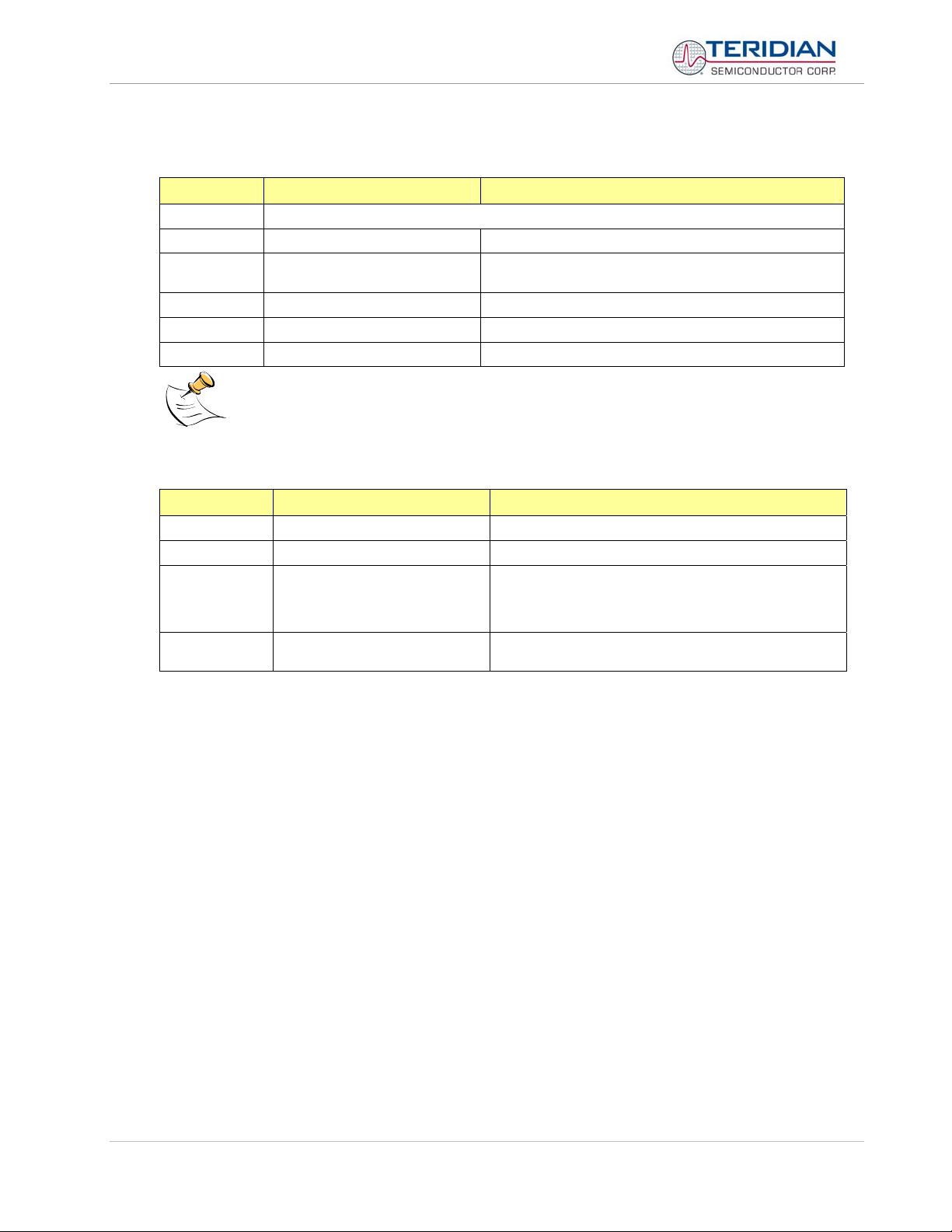
1.9 CALIBRATION PARAMETERS
1.9.1 GENERAL CALIBRATION PROCEDURE
Any calibration method can be used with the 71M6513/6513H chips. This Demo Board User’s Manual presents
calibration methods with three or five measurements as recommended methods, because they work with most
manual calibration systems based on counting "pulses" (emitted by LEDs on the meter).
Naturally, a meter in mass production will be equipped with special calibration code offering capabilities beyond
those of the Demo Code. It is basically possible to calibrate using voltage and current readings, with or without
pulses involved. For this purpose, the MPU Demo Code can be modified to display averaged voltage and
current values (as opposed to momentary values). Also, automated calibration equipment can communicate
with the Demo Boards via the serial interface and extract voltage and current readings. This is possible even
with the unmodified Demo Code.
A complete calibration procedure is given in section 0 of this manual.
Regardless of the calibration procedure used, parameters (calibration constants) will result that will have to be
applied to the 71M6513/6513H chip in order to make the chip apply the modified gains and phase shifts
necessary for accurate operation. Table 1-4 shows the names of the calibration constants, their function, and
their location in the CE RAM.
Again, the command line interface can be used to store the calibration constants in their respective CE RAM
addresses. For example, the command
>]8=+16302
stores the decimal value 16302 in the CE RAM location controlling the gain of the current channel (CAL_IA) for
phase A.
The command
>]9=4005
stores the hexadecimal value 0x4005 (decimal 16389) in the CE RAM location controlling the gain of the voltage
channel for phase A (CAL_VA).
CE
Constant
CAL_VA
CAL_VB
CAL_VC
CAL_IA
CAL_IB
CAL_IC
PHADJ_A
PHADJ_B
PHADJ_C
TEMP_NOM 0x11 TEMP_RAW reading
Address
(hex)
0x09
0x0B
0x0D
0x08
0x0A
0x0C
0x0E
0x0F
0x10
Description
Adjusts the gain of the voltage channels. +16384 is the typical value. The
gain is directly proportional to the CAL parameter. Allowed range is 0 to
32767. If the gain is 1% slow, CAL should be increased by 1%.
Adjusts the gain of the current channels. +16384 is the typical value. The
gain is directly proportional to the CAL parameter. Allowed range is 0 to
32767. If the gain is 1% slow, CAL should be increased by 1%.
This constant controls the CT phase compensation. No compensation
occurs when PHADJ=0. As PHADJ is increased, more compensation is
introduced.
Page: 28 of 112
Table 1-4: CE RAM Locations for Calibration Constants
© 2005-2006 TERIDIAN Semiconductor Corporation Revision 5.6

71M6513/71M6513H Demo Board User’s Manual
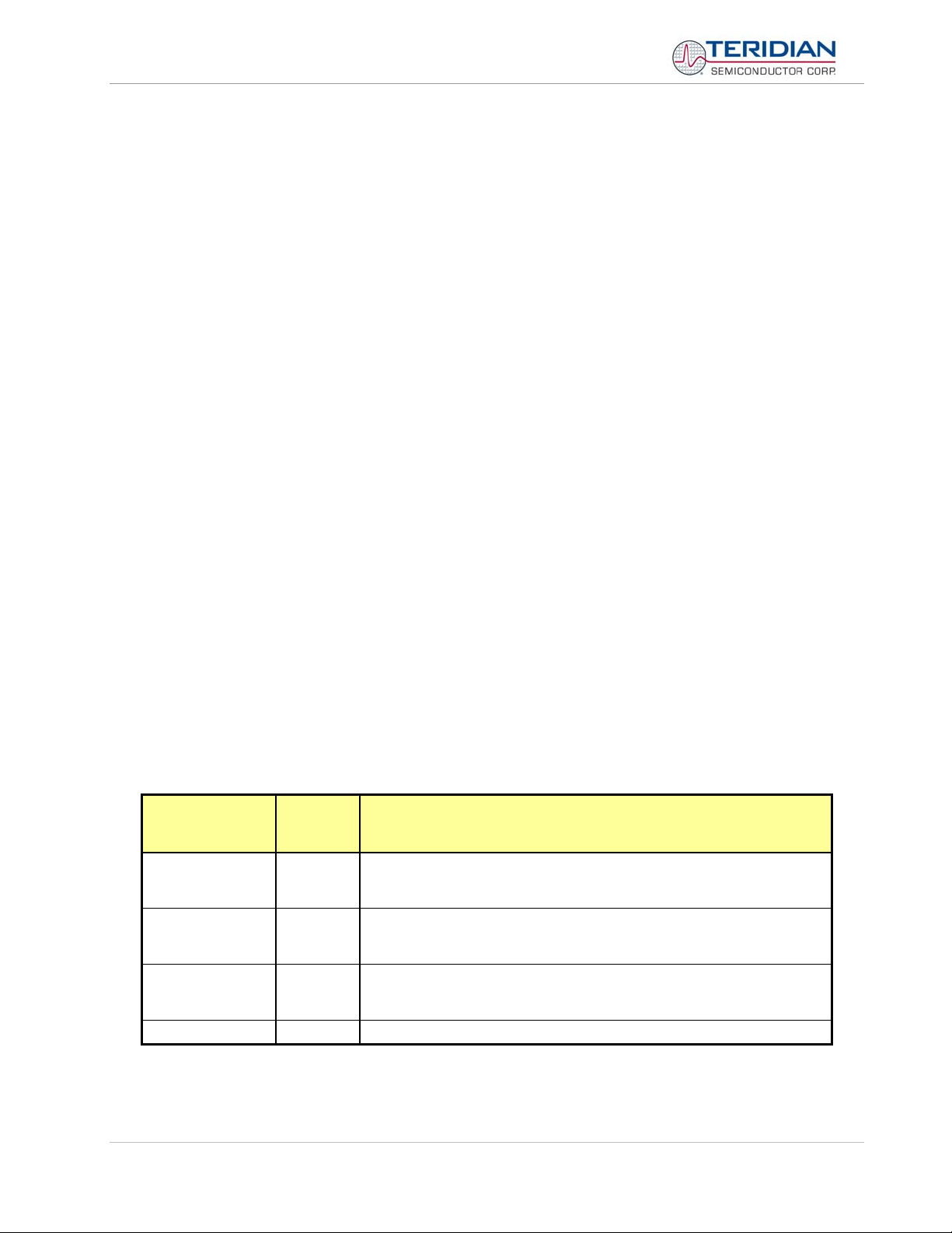
1.9.2 CALIBRATION MACRO FILE
The macro file in Figure 1-7 contains a sequence of the serial interface commands. It is a simple text file and
can be created with Notepad or an equivalent ASCII editor program. The file is executed with HyperTerminal’s
Transfer->Send Text File command.
]8=+16022/ CAL_IA (gain=CAL_IA/16384)
]9=+16381/ CAL_VA (gain=CAL_VA/16384)
]a=+16019/ CAL_IB (gain=CAL_IB/16384)
]b=+16370/ CAL_VB (gain=CAL_VB/16384)
]c=+15994/ CAL_IC (gain=CAL_IC/16384)
]d=+16376/ CAL_VC (gain=CAL_VC/16384)
]e=+115/ PHADJ_A (default 0)
]f=+113/ PHADJ_B (default 0)
]10=+109/ PHADJ_C (default 0)
ce1
Figure 1-7: Typical Calibration Macro file
It is possible to send the calibration macro file to the 71M6513/71M6513H for “temporary” calibration. This will
temporarily change the CE data values. Upon power up, these values are refreshed back to the default values
stored in flash memory. Thus, until the flash memory is updated, the macro file must be loaded each time the
part is powered up. The macro file is run by first issuing the ce0 command to turn off the compute engine and
then sending the file with the transfer
Æ
send text file procedure.
Æ
Use the Transfer
Send Text File command!
1.9.3 UPDATING THE 6513_DEMO.HEX FILE
The io_merge program updates the 6513_demo.hex file with the values contained in the macro file. This
program is executed from a DOS command line window. Executing the io_merge program with no arguments
will display the syntax description. To merge macro.txt and old_6513_demo.hex into new_6513_demo.hex, use
the command:
io_merge old_6513_demo.hex macro.txt new_6513_demo.hex
The new hex file can be written to the 71M6513/71M6513H through the ICE port using the ADM51 in-circuit
emulator. This step makes the calibration to the meter permanent.
1.9.4 UPDATING CALIBRATION DATA IN FLASH MEMORY WITHOUT USING THE
ICE OR A PROGRAMMER
It is possible to make data permanent that had been entered temporarily into the CE RAM. The transfer to flash
memory is done using the following serial interface command:
>]U
Thus, after transferring calibration data with manual serial interface commands or with a macro file, all that has
to be done is invoking the U command.
Similarly, calibration data can also stored in EEPROM using the CLS command.
Page: 29 of 112
After reset, calibration data is copied from the EEPROM, if present. Otherwise, calibration
data is copied from the flash memory. Writing 0xFF into the first few bytes of the EEPROM
deactivates any calibration data previously stored to the EEPROM.
© 2005-2006 TERIDIAN Semiconductor Corporation Revision 5.6

71M6513/71M6513H Demo Board User’s Manual
1.9.5 AUTOMATIC GAINS CALIBRATION
Starting with Demo Code revision 3.04, it is possible to perform a simple automatic calibration. This calibration
is performed for resistive loads only and will not correct phase angle
1. Enter operating values for voltage and current in I/O RAM. The voltage is entered at address 0x2029
(e.g. with the command
)29=+2400 for 240V), the current is entered at 0x202A (e.g. with the command
)2A=+300 for 30A) and the duration measured in accumulation intervals is entered at 0x2028.
2. The operating voltage and current defined in step 1 must be applied to the meter (Demo Board).
3. The CLB (Begin Calibration) command must be entered via the serial interface. The operating voltage
and current must be maintained accurately while the calibration is being performed.
4. The calibration procedure will automatically reset CE addresses 08, 09, 0x0A, 0x0B, 0x0C, and 0x0D
to nominal values (0x4000), and 0x0E, 0x0F and 0x10 to zero prior to starting the calibration.
Automatic calibration also reads the chip temperature and enters it in CE location 0x11 for proper
temperature compensation.
5. The LCD showing the “HELLO” message will signal completion of the automatic calibration. Enter M3
or another serial interface command to bring the display back to normal.
6. CE addresses 08, 09, 0x0A, 0x0B, 0x0C, and 0x0D will now show values other than 0x4000. These
values can be stored in EEPROM by issuing the CLS command.
Tip: Current transformers of a given type usually have very similar phase angle for identical operating
conditions. If the phase angle is accurately determined for one current transformer, the corresponding
phase adjustment coefficient PHADJ_X can be entered for all calibrated units.
. The steps required for the calibration are:
1.9.6 LOADING THE 6513_DEMO.HEX FILE INTO THE DEMO BOARD
Hardware Interface for Programming: The 71M6513/6513H IC provides an interface for loading code into the
internal flash memory. This interface consists of the following signals:
E_RXTX (data)
E_TCLK (clock)
E_RST (reset)
These signals, along with V3P3 and GND are available on the emulator header J14. Production meters may be
equipped with much simpler programming connectors, e.g. a 5x1 header.
Programming of the flash memory requires a specific in-circuit emulator, the ADM51 by Signum Systems
(http//www.signumsystems.com) or the Flash Programmer (TFP-1) provided by TERIDIAN Semiconductor. A
gang programmer is available for high-volume production.
In-Circuit Emulator: If firmware exists in the 71M6513/6513H flash memory, this memory has to be erased
before loading a new file into memory. Figure 1-8 and Figure 1-9 show the emulator software active. In order to
erase the flash memory, the RESET button of the emulator software has to be clicked followed by the ERASE
button (Figure 1-8).
Once the flash memory is erased, the new file can be loaded using the commands File followed by Load. The
dialog box shown in Figure 1-9 will then appear making it possible to select the file to be loaded by clicking the
Browse button. Once the file is selected, pressing the OK button will load the file into the flash memory of the
71M6513/6513H IC.
At this point, the emulator probe (cable) can be removed. Once the 71M6513/6513H IC is reset using the reset
button on the Demo Board, the new code starts executing.
Flash Programmer Module (TFP-1): Follow the instructions given in the User Manual for the TFP-1.
Page: 30 of 112
© 2005-2006 TERIDIAN Semiconductor Corporation Revision 5.6
 Loading...