

Page 1

Simplifying System In tegrationTM
73S8024C
Demo Board User Manual
November 11 , 2009
Rev. 1.3
UM_8024C_061
Page 2

73S 8024C Demo Board User Manual UM_8024C_061
© 20 09 Teridi an Semiconductor C or porati on. All rights r eserved .
Terid i an Semiconductor Corporation is a r egistered trademark of Teridi an Semiconductor Corporation.
Simplifying System Integ r ation i s a trademark of Teridian S emiconduct or C or poration .
All other trademarks ar e the property of thei r r espective owners.
Terid i an Semiconductor Corporation m akes no warranty for the use of i ts p r oduct s, other than expr essly
contained in the Comp any’s warranty d etailed in the Terid ian S emiconductor Corporation st andar d Terms
and C onditions. The company assu mes no responsib i lity for any errors whi ch may appear in this
document, reserves th e r i ght to change device s or sp ecifications detailed herein at any time withou t
notice and does n ot make any commitm ent to upd ate the information contained herein. Accordingl y, the
reader is cautioned to verify that t his document is current by comparing it to the latest version on
http://www.teridian .com or by checking with your sales represen tative.
Terid i an Semiconductor Corp., 64 40 Oak Canyon, Suite 100, Ir vine, CA 92618
TEL (714) 508-8800, FAX (714) 508-8877, http://www.teridian.com
2 Rev. 1.3
Page 3

UM_8024C_061 73S8024C Dem o Boar d User M anual
Table of Contents
1
Introduction ................................................................................................................................... 5
1.1 Packa ge Con tents.................................................................................................................... 5
1.2 Safet y and E SD Notes ............................................................................................................. 5
2 Basic Connections ........................................................................................................................ 6
3 Hardware Description .................................................................................................................... 7
3.1 Demo Board C onnectors, Jump er s and Test Poin ts ................................................................. 7
3.2 Recommended Op er ating Conditions and Absolut e M aximum Rat ings ..................................... 9
3.3 73S8024C Pin Description ....................................................................................................... 9
3.4 73S8024C Pinout .................................................................................................................. 11
4 Design Considerations ................................................................................................................ 12
4.1 Gener al Layout Rules ............................................................................................................ 12
4.2 Optimization for Compliance with EMV and NDS .................................................................... 12
5 73S8024C Demo Board Schematics, PCB Layouts and Bill of Materials .................................. 13
5.1 Schematic .............................................................................................................................. 13
5.2 Bill of Materials ...................................................................................................................... 14
5.3 PCB Layouts .......................................................................................................................... 15
6 Ordering Information ................................................................................................................... 18
7 Related Documentation ............................................................................................................... 18
8 Contact Information ..................................................................................................................... 18
Revision H istory .................................................................................................................................. 19
Rev. 1.3 3
Page 4

73S 8024C Demo Board User Manual UM_8024C_061
Figures
Figure 1: 73S8024C Demo Board
Figure 2: 73S8024C Demo Board Basic Connections
Figure 3: 73S8024C Demo Board Connectors, Jumper s and Test Points
Figure 4: 73S8024C SO28 Pinout (Top View)
Figure 5: 73S8024C Demo Board Electrical Schematic
Figure 6: 73S8024C Demo Board Top View
Figure 7: 73S8024C Demo Board Bottom View
Figure 8: 73S802 4C Demo Board Top Sign al Layer
Figure 9: 73S8024C Demo Board Middl e Layer 1, Grou nd Plane
Figure 10: 73S8024C Middle Layer 2, Supply Plane
Figure 11: 73S8024C D em o Board Bott om Sign al Layer
Tables
Table 1: 73S8024C Dem o Board Con nect or , Jumper and Test P oi nts
Table 2: Recommended Operating Conditi ons
Table 3: Absolu te Maxim um Ratings
Table 4: 73S8024C Card Interface Pins
Table 5: 73S8024C Misce llaneous Pi ns
Table 6: 73S8024C Power and Ground Pins
Table 7: 72S8024C Microcont r ol ler In terface Pins
Table 8: 73S8024C Dem o Board Bi l l of Materials
Table 9: Order Numbers and Packagin g Marks
............................................................................................................ 5
.............................................................................. 6
................................................. 8
........................................................................................ 11
.......................................................................... 13
........................................................................................... 15
...................................................................................... 15
............................................................................... 16
........................................................... 16
.............................................................................. 17
........................................................................ 17
...................................................... 7
......................................................................................... 9
........................................................................................................ 9
................................................................................................... 9
................................................................................................. 10
.......................................................................................... 10
.................................................................................. 10
................................................................................... 14
...................................................................................... 18
4 Rev. 1.3
Page 5
UM_8024C_061 73S8024C Dem o Boar d User M anual
1 Introduction
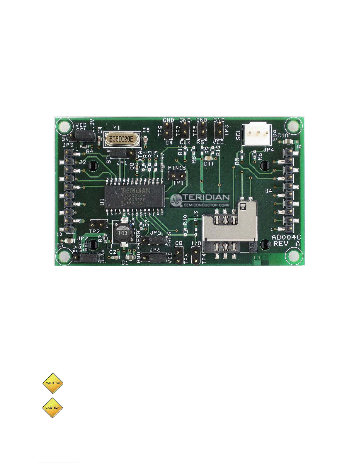
The 73S8024C Demo Board is a pl atform for evaluating th e Teridian 73S8024C Smart Card Interface
device. The board incorporates the 73S802 4C integrated circuit and has been d esigned to operate either
as a st andal one platform ( to be used in conju nction with an extern al microcontroller) or as a daught er
card to be used in conjunction with the 73S1121F evaluation platform.
The board has been designed to comply with the EMV 2 000 Specification, Version 4.0. 73S8024C Demo
Boards can easily be mod i fi ed to comply with NDS specifications by replacing a few external com ponents
that are highlighted in this document.
Figure 1: 73S8024C Demo Boa rd
1.1 Package Contents
The 73S8024C Demo Board Kit includes:
• A 73S8024C Demo Board
• The following documents on C D:
• 73S8024C Data Sheet
• 73S8024C Demo Board Us er Ma n ual (this document)
• Application Note
1.2 Safety an d ES D Notes
Extreme caution should be taken when handling the 73S8024C Demo Board afte r
connection to live voltages!
The 73S8024C Demo Board is ESD sensitive! ESD precautions should be taken when
handling this board!
Rev. 1.3 5
Page 6
73S 8024C Demo Board User Manual UM_8024C_061
1
2
CKDIV2
CKDIV1
RSTIN
CMDVCC
GND
VDD
PWRDN
5V/#V
GND
SCLK
OFF
I/OUC
AUX1UC
AUX2UC
External clock source. JP1 must be in
position SCLK when using an
external clock. Otherwise, pin SCLK
can be left open.
V
PC
Power
Supply:
Configure JP2
to 3.3V
V
DD
Power Supply:
+2.7V to +3.6V
(3.3V Typ.) / 50mA
Note: CLKSTOP and CLKLEV
can be left NC if unused.
5V/#V too, for 5V cards only.
2 Basic Connections
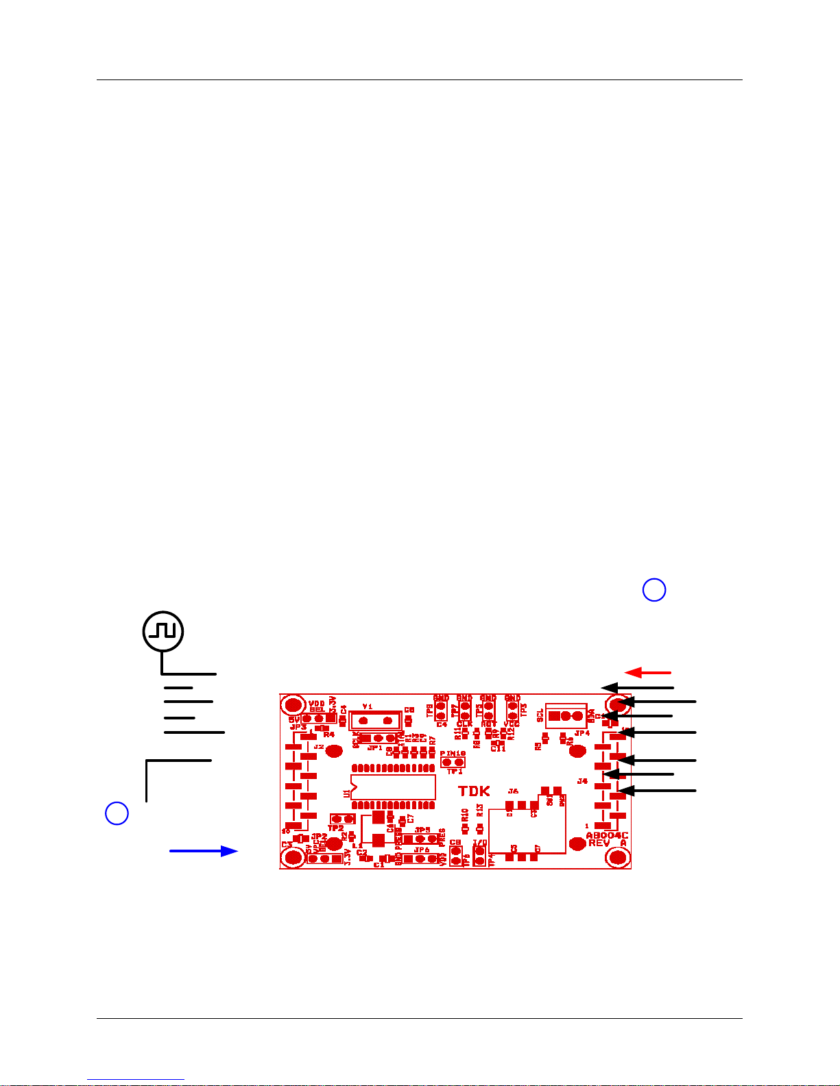
The basic connections to the demo boar d are d escribed below and shown in Figure 2.
1. Connect power supply: Apply 3.3 V to pin 10 of J4.
2. Control signals to the device can be co nnected through J2 and J4 (see Figure 2 and the Electrical
Schematic, Figure 5).
3. To set the clock frequency with an extern al cl ock source:
• Set JP1 to the SCLK setting.
• App l y clock source to pin 1 of J2.
• Apply 3.3V (1) or GND (0) to CLKDIV1 and CLKDI V2 pins to set the desi r ed clock rate as follows:
CLKDIV1 = CLKDIV2 = 0 clock frequency = SCLK/8
CLKDIV1 = 0, CLKDIV2 =1 clock frequency = SCLK/4
CLKDIV1 = 1, CLKDIV2 =0 clock frequency = SCLK
CLKDIV1 = CLKDIV2 = 1 clock frequency = SCLK/2
4. To set the clock frequency using crystal Y1:
• The crystal included on the demo board is 12 MHz.
• Set JP1 to XTAL position.
• Apply 3.3V (1) or GND (0) to CLKDIV1 and CLKDIV2 pins to set the desired clock r ate as fol lows:
CLKDIV1 = CLKDI V2 = 0 clock frequency = 1.5 MHz
CLKDIV1 = 0, CLKDIV2 =1 clock frequency = 3 MHz
CLKDIV1 = 1, CLKDIV2 =0 clock frequency = 12 MHz
CLKDIV1 = CLKDIV2 = 1 clock frequency = 6 MHz
Figure 2: 73S8024C De mo Board Basic Connections
6 Rev. 1.3
Page 7
UM_8024C_061 73S8024C Dem o Boar d User M anual
Schematic/
Connectors:
CLKDIV2 and CLKDIV1.
(under neath the P CB) . No SIM / SAM sh o uld be inse r t e d
when using the credit-card size connector J5.
3 Hardware Description
3.1 Demo Board C onne ctors, Ju mpers an d Test Poi n ts
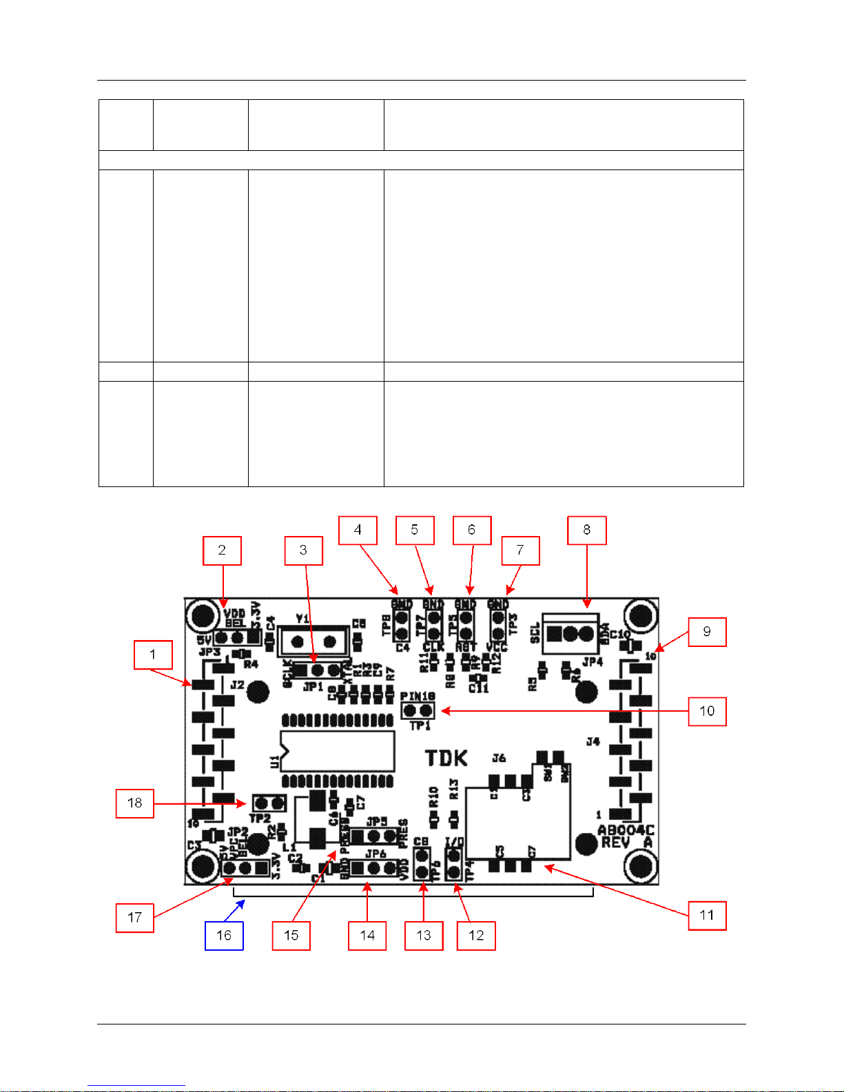
Table 1 describe s the 73S8024C Demo Board connectors, jump er s and t est points. The Item # in Table 1
refers to Figure 3.
Table 1: 73S8024C Demo Board Connector, Jumper and Test Points
Item
#
1 J2 5V Board Supply /
9 J4 3.3V Board Power /
16 J5 Smart Card
11 J6 Smart Card
Jumpers:
3 JP1 Clock Selection Jumper to select between a crysta l or an external clock
17 JP2 VPC Sel e ct Jumper to select the value of the power supply for the
2 JP3 VDD Select Jumper to select th e digital voltag e wh ich supp lies the
8 JP4 – Not used.
15
14
Silkscreen
Reference
JP5
JP6
Name Function
73S8024C auxiliary interface (I/OUC, AUX1UC,
Auxiliary Interface
Digital Control
Signals
Connector
Connector
Card Polarity
Detect Select
AUX2UC), external clock (SCLK) and interrupt (OFF)
pins. The external clock ( SCLK) can be left open when
JP1 is in position XTAL.
The 5V power supply is unused and must be left open
and JP2 m ust be inse r t e d i n po sition 3.3V.
3.3V board power supply and the 73S8024C host
control sign als RSTIN, CMDVCC, 5V /#V, PWRDWN,
Smart card connector.
When inse r ting a card (credit card si ze format), contacts
must face up.
SIM /SAM smart card form at con nect or .
J6 i s wired in parall el to the smart car d connector J5
as the frequency reference to the device. The default
setting is for a cr ystal.
smart card DC-DC converter ( 73S8024C input VPC).
To sup port both car d voltages, JP2 must be se t to
position 3.3V. The default setting is 3.3V.
73S8024C. Must be set for 3.3V.
The setting of JP5 and JP6 depends on the type of
smar t card connector used (nominall y open or closed)
and which 73S8024C card presen ce switch inp ut is
used. The switch is nominally open for the 73S8024C
Demo Board. The jumpers can be set to:
Rev. 1.3 7
1. Use of PR ES (default): JP5 set to PRES; JP6 set
to VDD.
2. Use of PRES: JP5 set to PRE B; JP6 set to GND.
Page 8
73S 8024C Demo Board User Manual UM_8024C_061
Schematic/
Test Points:
deter mination of the r esistor values.
Item
#
Silkscreen
Reference
Name Function
10 TP1 Pin 17 (VDDF_ADJ) VD D voltage fault adjustment. The pin to the left is
connected to the VDDF_ADJ pin of the 73S8024C and
the pin to the rig ht is GND. When either a r esist or R 3,
or a resistor network R1 and R3 is populated on the
board, it adjusts the VDD fault l evel that internally
triggers a card deacti vation se quence.
By default, the resistor s R1 and R3 are n ot con nect ed.
This provides a VDD fault level of 2.3V typical (internally
set to the 73S8024C). Refer to the 73S8024C Data
Sheet for further information about VDD fault level and
20 TP2 Factory Test Factory test pin. Do not conn ect.
7
12
6
13
5
4
TP3
TP4
TP5
TP6
TP7
TP8
VCC
I/O
RST
C8
CLK
C4
2-pin test points for each respective smar t card sig nal.
The pin lab el nam e i s the respect ive signal (i. e. VCC ,
CLK) and th e 2nd pin is GND.
Figure 3: 73S8024C Demo Board Connectors, Jumpers and Te st Points
8 Rev. 1.3
Page 9
UM_8024C_061 73S8024C Dem o Boar d User M anual
Parameter
Rating
Name
Pin #
Description
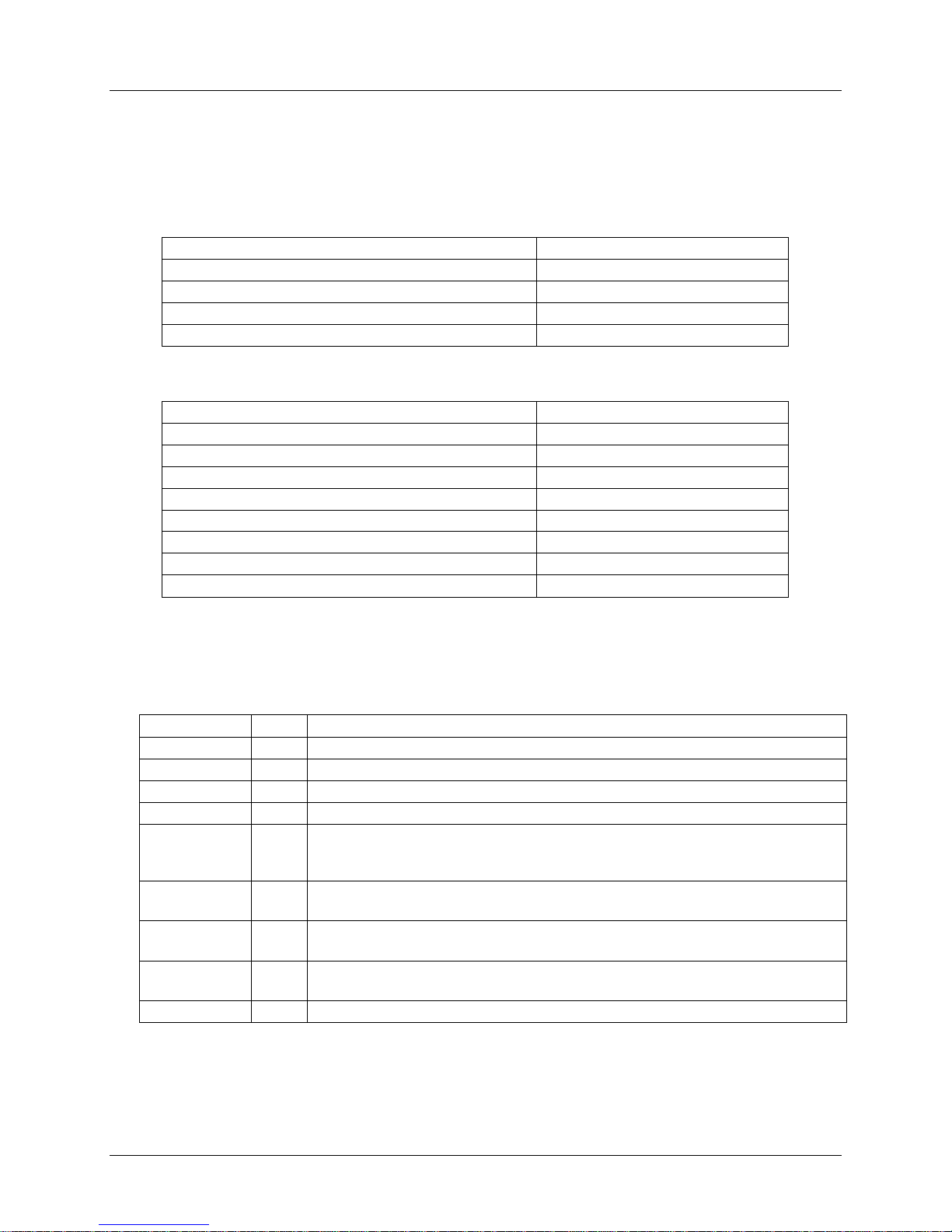
3.2 Recommended Operating Conditions and Absolute Maximum Ratings
Table 2 l i sts the recommended operating co nditi ons and Table 3 list s t he absolute maximum rati ngs.
Oper ation outside th ese rating limits may cause perm anent damage to the d evice.
Table 2: Recommended Operating Conditions
Parameter Rating
Sup ply Voltage VDD 2.7 to 3.6 VDC
Sup ply Voltage VPC 2.7 to 3.6 VDC
Ambient Operating Temperature -40 °C to +85 °C
Input Voltage for Di gital Inputs 0 V to VDD + 0.3 V
Table 3: Absolute Maximum Ratings
Sup ply Voltage VDD -0.5 to 4.0 VDC
Sup ply Voltage VPC -0.5 to 4. 0 VDC
Input Voltage for Di gital Inputs -0.3 to (VDD+0.5) VDC
Stor age Temperature -60 °C to 150 °C
Pin Voltage -0.3 to (VDD+0.5) VDC
Pin Current ±100 mA
ESD Toleran ce – Card interface p i ns +/- 6 kV
ESD Toleran ce – Other pins +/- 2 kV
ESD testing on Car d pins is HBM condition, 3 pulses, each polarity refer enced to grou nd.
3.3 73S8024C Pin Des cript i on
Table 4: 73S8024C Card Interface Pins
I/O 11 Card I /O: Data sig nal to/from card. Includes a pul l -up resistor to V
AUX1 13 AUX1: Auxili ary data sig nal to/from card. Includes a pull-up resistor to V
AUX2 12 AUX2: Auxili ary data sig nal to/from card. Includes a pull-up resistor to V
RST 14 Card rese t: provides r eset (RST) si gnal to card.
CLK 15 Card clock: provides clock signal ( C LK) to card. The rate of this clock is
deter mined by crystal osci llator frequen cy or ext er nal clock inpu t and
CLKDIV selections.
PRES 10 Card Presence switch: active hi gh i ndicates card is present. Should be tied
to GND when not used, but it includes a high-impedance pull-down resistor.
PRES 9 Card Presence switch: active low indicates card is prese nt. Should be tied
to V
when not used, but it include s a hi gh-impedance pull-up resistor.
DD
VCC 17 Card power supply: logica lly controlled by sequencer output of LDO
regulator. Req uires an extern al filter cap acitor to t he card GND.
GND 14 Card grou nd.
CC.
CC.
CC.
Rev. 1.3 9
Page 10
73S 8024C Demo Board User Manual UM_8024C_061
Name
Pin #
Description
19
Command VC C ( negative assertion): Logic low on this pin ca uses the LDO
When the part is to be used with
CLKDIV1
CLKDIV2
CLOCK RATE
0 1 XTALIN/4
1 1 XTALIN/2
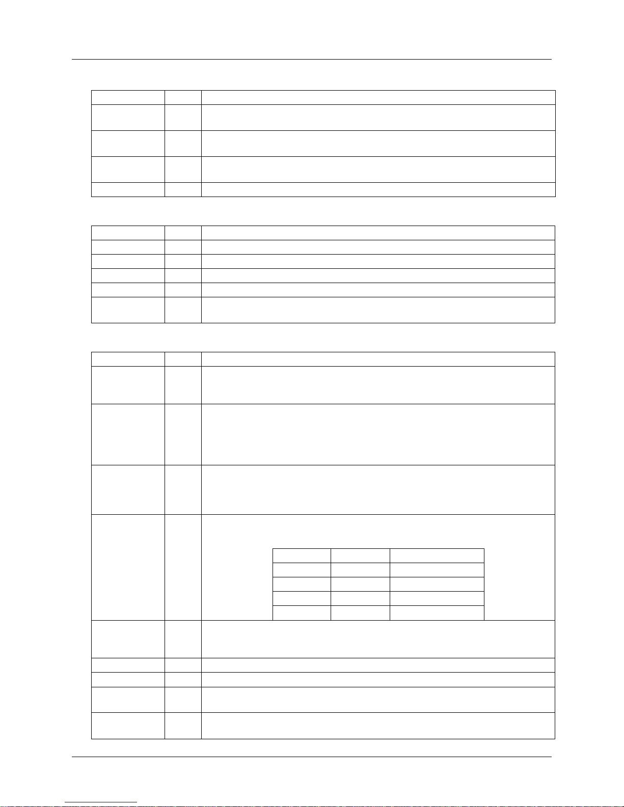
Table 5: 73S8024C Miscellaneous Pins
Name Pin # Description
XTALIN 24 Crystal oscillator inp ut: can either be connected to crystal or driven as a
source for th e card clock.
XTALOUT 25 Crystal oscillator output: connected to cr ystal. Left op en if XTA LIN is being
used as external clock in put.
VDDF_ADJ 18 VDD fault threshold adj ustment input: this pin ca n be used to adjust the V
DDF
values (con trols deact i vation of the card). Must be left open if unused.
NC 5,7 Non-connected pin.
Table 6: 73S8024C Power and Ground Pins
VDD 21 System interface supply voltage and supply voltage for internal cir cuitry.
VPC 6 DC-DC converter power supply source.
GND 4 DC-DC converter ground.
GND 22 Digital grou nd .
LIN 5 External inductor. Connect external in duct or from p i n 2 to VPC. Keep the
inductor close t o pin 2.
Table 7: 72S8024C Micro co nt r ol l er In ter face Pins
Name Pin # Description
CMDVCC
regulator to ramp the VCC supply to the card and initiates a card activation
sequence , if a card is p r esent .
5V/#V 3 5 volt / 3 volt card se lection: Logic one selects 5 volts for VCC and card
interface, logi c low selects 3 volt op er ati on.
a sin gle card voltage, this pin should be tied to either GND or VDD. However,
it includes a high impedance pull-up resistor to default this pin high
(selection of 5V card ) wh en not connected.
PWRDN 8 Power Down control input. Active high. When th e Power Down mod e i s set
high, all internal analog functi ons are disabled to place the 73S8024C in i ts
lowest power consumption mode. The Power Down mode i s only allowed
out of a card session (i.e. when CM D VCC = 1)
CLKDIV1
CLKDIV2
1 2 Sets the d i vide rati o from the XTAL osci llator (or external clock input) to the
card clock. These pins include pull-down resistors.
0 0 XTALIN/8
1 0 XTALIN
OFF 23 Int er r upt signal to the p r ocessor. Active low - multi-funct ion indicating fault
conditi ons and /or card presence. Open drain output configuration; includes
an internal 22 kΩ pull-up to V
DD.
RSTIN 20 Reset Input: This signal is the reset command to the card.
I/OUC 26 System co ntroller data I/O to/from the car d. Includes a pull-up resistor to V
DD.
AUX1UC 27 System controller auxili ary data I/O to/ from the card. Includes a pull-up
resistor to V
DD.
AUX2UC 28 System controller auxili ary data I/O to/ from the card. Includes a pull-up
resistor to V
DD.
10 Rev. 1.3
Page 11
UM_8024C_061 73S8024C Dem o Boar d User M anual
CLKDIV1
CLKDIV2
5V/#V
GND
VPC
PRES
PRES
I/O
AUX2
AUX1
GND
AUX2UC
AUX1UC
I/OUC
XTALIN
XTALOUT
OFF
VDD
RSTIN
CMDVCC
VCC
RST
CLK
NC
LIN
PWRDN
VDDF_ADJ
GND
73S8024C
1
18
17
16
15
14
13
12
11
10
9
8
7
6
5
4
3
2
19
20
28
27
26
25
24
23
22
21
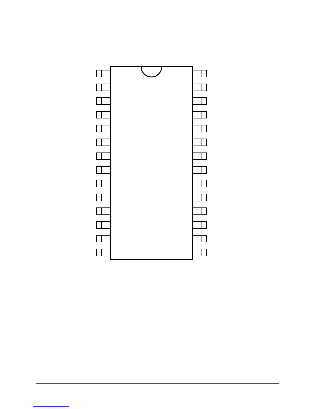
3.4 73S8024C Pinout
Figure 4: 73S8024C SO28 Pinout (Top View)
Rev. 1.3 11
Page 12

73S 8024C Demo Board User Manual UM_8024C_061
4 Design Considerations
4.1 General Layout Rules
• Route the auxiliary signals away from card interface signal s.
• Keep the CLK signal as short as possible and with few bends in the t r ace. Keep the route of th e CLK
trace to one layer (avoid vias to ot her p l ane). Keep the CLK trace a way from other traces, especially
RST and VCC. Filter i ng of the CLK trace is al lowed for noise pu r pose. U p to 30 pF to gr ound i s
allow ed at the CLK pin of the sm ar t card connector. In addition, the zero ohm seri es resistor, R 7, ca n
be replaced for addi tional filt er i ng ( no mor e than 100 Ω).
• Keep the VCC trace as shor t as p ossible. Make the trace a minimum of 0.5 mm thick. In addition,
keep the VCC away fr om other traces, especially RST and CLK.
• Keep the trace from L1 to pin 5 of the IC as sh or t as p ossib le.
• Keep the RST trace a way from the VCC and CLK traces. Up to 30 pF to ground is allo w ed for
filtering.
• Keep the 0.1 µF capacitor close to the VDD pin of the device and dir ectly take the other end to
ground.
• Keep the 0.1 µF capacitor close to the VPC pin of th e device and directly take the other end to
ground.
• Keep the 3.3 µF (1.0 µF for NDS) capacitor close to the VC C pin of t he smart card connector and
directly take other end to ground.
4.2 O ptimization for Compliance with EMV and NDS
The default configuration of the demo board contains a 27 pF capacitor (C12) from the CLK pin of the
smar t conn ector t o grou nd and a 27 pF capacitor (C13) from the RST pin of th e smart con nect or to
ground. These capacitor s serve as filters for the C LK and RST sig nals i n the case of long traces or test
equipment perturbati ons. The capacitor on CLK reduces r ing in g on the trace, r educes coupling to other
traces and slows down the edge of t he CLK signal. The capacit or on RS T helps the perturbation
specification in a noisy environment. The filt er capacitors can be useful in the EMV test environment and
have no effect on NDS testing .
C12 and C13 are r epresented on both the schematic and the BOM. These ca pacitors are optional filter
capacitors on the smart card lines CL K and RST, r espectively for each card interface. These capacitors
may be adju sted ( value not to exceed 30 p F) or rem oved to op tim i ze performance in each specific
app l ication (PCB, card clock frequency, compli ance with applicable standards etc).
The default VCC capaci tor of 3.3 µF is requi r ed to meet the d ynamic VCC (smar t card suppl y) transient
curr ent requir ement as specified in the EMV2000 version 4 .0 specification. For compl iance wit h NDS, a
smaller capacitor of 1 µF is r equi r ed to meet the activat ion d ischarge t ime specification.
12 Rev. 1.3
Page 13
UM_8024C_061 73S8024C Demo Board User M anual
Rev. 1.3 13
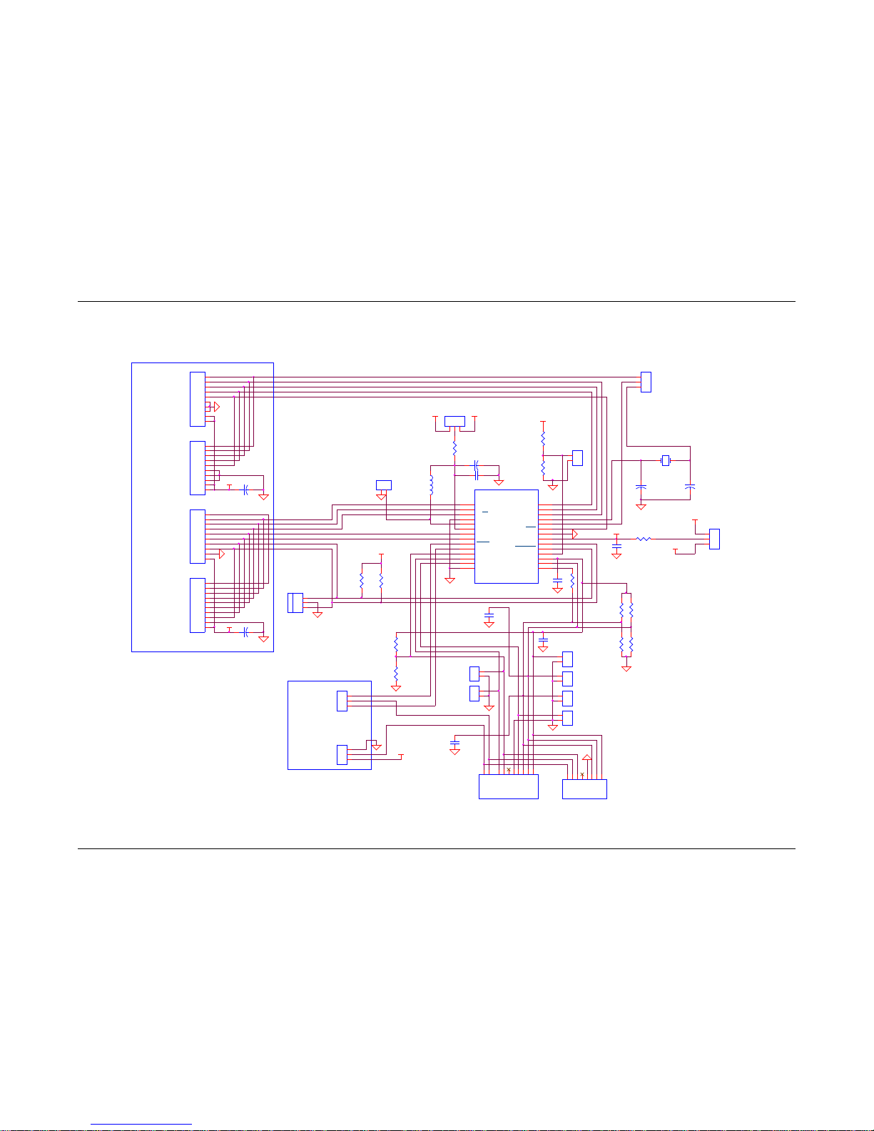
5 73S8024C Demo Bo ard S ch ematics, PCB Layouts and Bill of Materials
5.1 Schematic
USR3
CLK
GND
JP6
1
2
3
PGND
5V
C4
22pF
J4
TSM_110_01_L_SV
1
2
3
4
5
6
7
8
9
10
SC4
3.3V
R8
Ru
TP6
1
2
VDD
USR5
C4
VPC
R10
Ru
Resistors
not
populated
+
C10
10uF
3.3V
GND
C11
0.1uF
Connectors are positioned to allow
multiple 8024C boards (stacking) to a
73S1121F evaluation board. Also used for
connecting external signals when used as a
stand alone board.
JP4
HEADER LOC K 3
1
2
3
CLKDIV1
GND
USR2
+
C1 10uF
JP2 must be
set to 3.3V
Card detection
switches are
normally open
CARD DETECT
POLARITY SELECT
I/O
VDD
R11
Rd
SIO
L1
10uF
R2
0
R5
R7
0
R12
Rd
C8
GND
5.0V
TP7
1
2
JP2
123
R13
Rd
USR1
3.3V
C2 0.1uF
R6
OFFB
R4
0
C8
0.1uF
C1, C2, C8, C9 and L1 must be
placed within 5mm of the U1 pins
and connected by thick track
(wider than 0.5mm)
5V
S_C8
Resistors not
populated
U1
73S8024C
1
2
3
4
5
6
7
12
8
9
10
11
13
14 15
16
17
18
19
20
21
22
23
28
27
25
24
26
CLKDIV1
CLKDIV2
5V3V
GND_4
LIN
VPC
NC
AU X2
PWRDN
PRES
PRES
I/O
AU X1
GND_14 CLK
RST
VCC
VDDF_ADJ
CMDVCC
RSTIN
VDD
GND
OFF
AUX2UC
AUX1UC
XTALOUT
XTAL IN
I/OUC
JP3 must be
set to 3.3V
J5
Smart Card C onnec t or
123456789
10
VCC
RST
CLK
C4
GND
VPP
I/O
C8
SW-1
SW-2
SIO
TP2
1
2
CLKDIV2
JP3
1
2
3
3.3V
J2
TSM_110_01_L_SV
1
2
3
4
5
6
7
8
9
10
+
C3
10uF
5.0V
TP8
1
2
SC8
5V3VB
3.3V
TP4
1
2
PIN18
Signal names
refer to
73S1121F
Evaluation
board.
GND
NC
USR6
JP5
1
2
3
VDD
C5
22pF
5V
XTALIN
SELECT
GND
PWRDN
USR4
J1
SSM_110_L_SV
1
2
3
4
5
6
7
8
9
10
SCLK
R9
Ru
TP1
1
2
SCLK
VDD
SELECT
Signal names
refer to
73S1121F
Evaluation
board.
VDD
CMDVCCB
TP5
1
2
XTAL
TP3 to TP8 to be placed
very close to the pads
of J5
R3
J6
SIM/SAM Connector
1234567
8
C1C2C3C5C6
C7
SW1
SW2
SCLK
+5V
TP3
1
2
RSTIN
L1 must be
placed close
to pin 5
VPC
SELECT
INT2
PRESB
S_C4
+5V
JP1
1
2
3
GND
PRES
J3
SSM_110_L_SV
1
2
3
4
5
6
7
8
9
10
VCC
C9
0.47uF
+3.3V
VDD
C13
27pF
R1
RST
Y1
12.000MHz
1 4
C12
27pF
5.0V
USR7
USR0
Figure 5: 73S8024C Demo Board Electrical Schematic
Page 14
73S8024C Demo Board User M anual UM_8024C_061
14 Rev. 1 .3
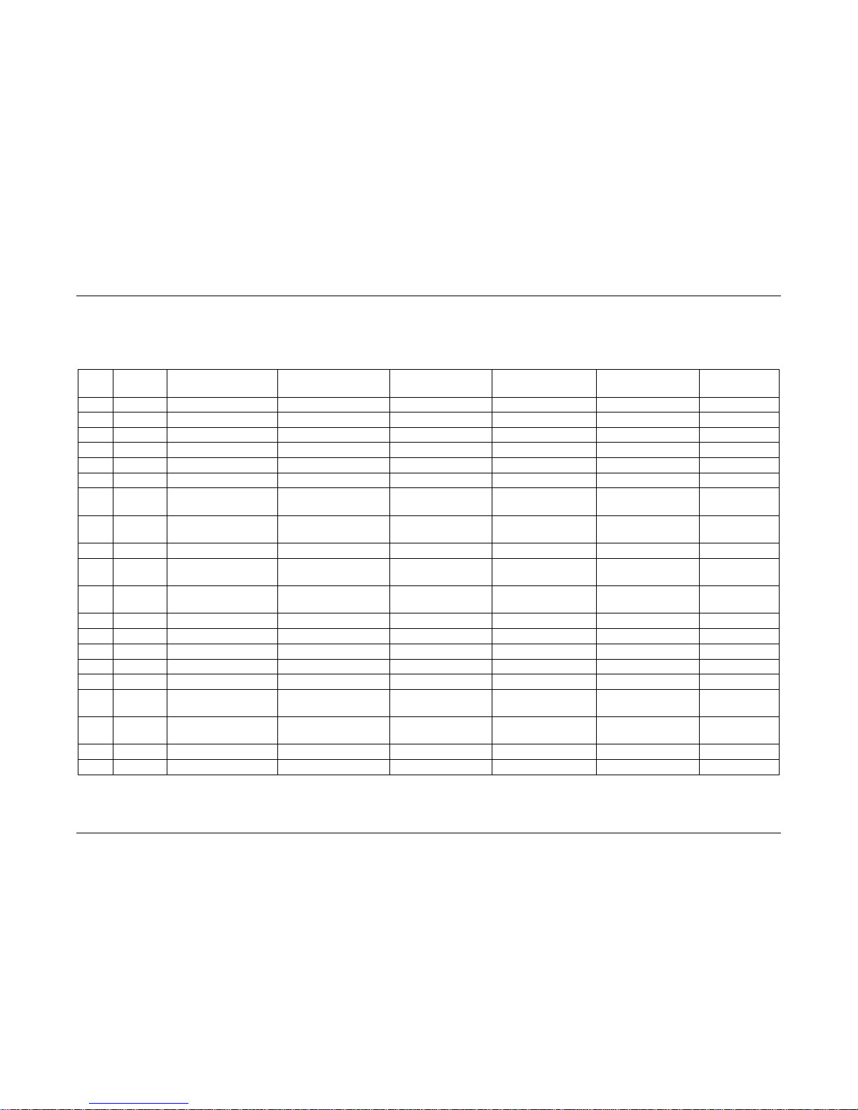
5.2 Bill of Materials
Table 8 p r ovides the bi l l of materials for the 73S 8024C Dem o Board schematic provided in Figure 5.
Table 8: 73S8024C Demo Board Bill of Materials
Item Quantity Reference Part PCB Footprint
Digikey Part
Number
Part Number Manufacturer
1 3 C1,C3,C10 10 µF 805 PCC2225CT-ND ECJ-2FB0J106M Panasonic
2 2 C2,C8 0.1 µF 603 PCC1762CT-ND ECJ-1VB1C104K Panasonic
3 2 C4,C5 22 pF 603 PCC220ACVCT-ND ECJ-1VC1H220J Panasonic
4 1 C11
3.3 µF
805
PCC1925CT-ND
ECJ-2YB0J335K
Panasonic
5 2 C12, C13 27 pF 402 PCC270CQCT-ND ECJ-0EC1H270J Panasonic
6 1 L1 10 µH X SLF6025 TDK
7 5 JP1,JP2,JP3,JP5,
JP6
HEADER 3 3pins, 2.54 mm
pitch
S1011-36-ND PZC36SAAN Sullins
8 1 JP4
Header L ock 3
3pins, 2.54 mm
pitch
WM2701-ND
22-11-2032
Molex
9 2 J1,J3 SSM_110_L_SV SSM_110_L_SV X SSM_110_L_SV Samtec
10 2 J2,J4 TSM_110_01_L_SV TSM_110_01_L_SV X TSM_110_01_L_SV Samtec
11 1 J5 Smart Card
Connector
ITT_CCM02-2504 ccm02-2504-ND ccm02-2504 ITTCannon
12 1 J6 SIM/SAM Connector ITT_CCM03-3754 CCM03-3754CT-ND CCM03-3754 ITTCannon
13 3 R2,R4,R7 0 603 P0.0GCT-ND ERJ-3GEY0R00V Panasonic
14 2 R5,R6 X 603 X X
15 4 R1,R8,R9,R10 Ru 603 X X
16 4 R3,R11,R12,R13 Rd 603 X X
17 8 TP1,TP2,TP3,TP4,
TP5,TP6,TP7,TP8
TP2 2X1_Header S1011-36-ND PZC36SAAN Sullins
18 1 U1 73S8024C 28SOP X 73S8024C Teridian
Semiconductor
19 1 Y1
12.000 MHz
HC-49US
X190-ND
ECS-120-20-4DN
ECS
20 2 C4,C5 22 pF 603 PCC220ACVCT-ND ECJ-1VC1H220J Panasonic
1
Ru and Rd are not populated on the board. They can be implemented to ad j ust the features of the smart card reader.
Page 15
UM_8024C_061 73S8024C Demo Board U ser Manual
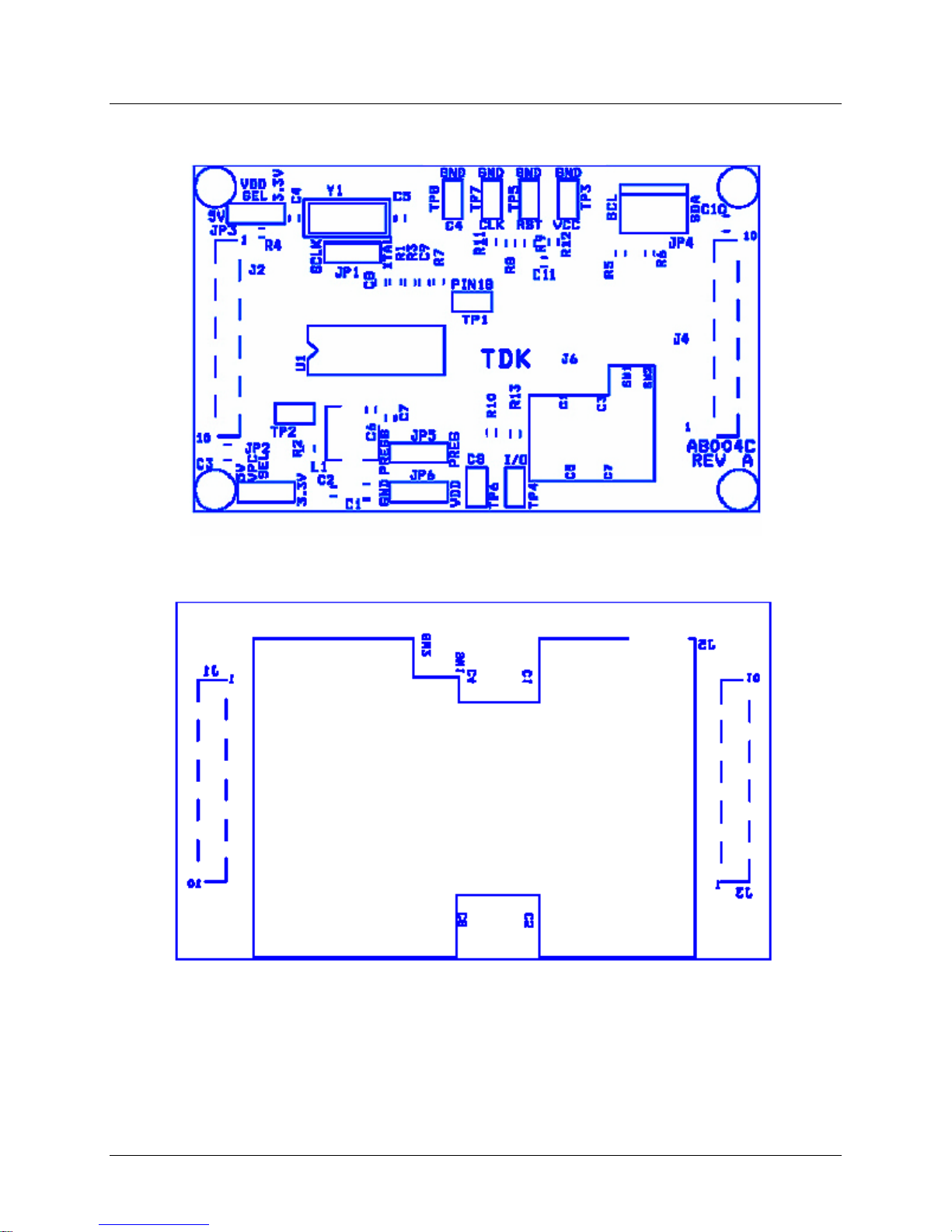
5.3 PCB Layouts
Figure 6: 73S8024C Demo Board Top View
Figure 7: 73S8024C Demo Board Bottom View
Rev. 1.3 15
Page 16
73S 8024C Demo Board User Manual UM_8024C_061
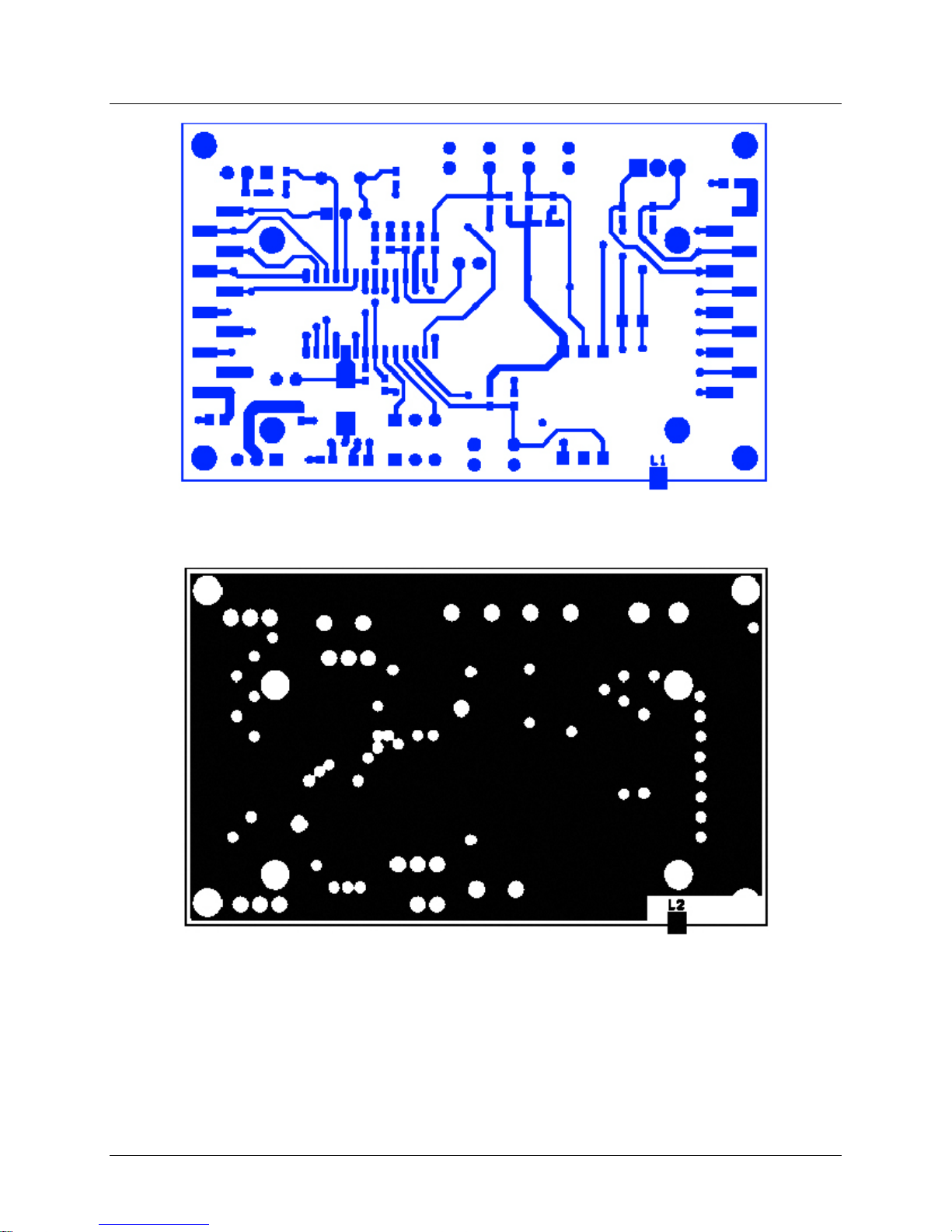
Figure 8: 73S8024C De mo Board Top Signal Layer
Figure 9: 73S8024C De mo Board Middle Layer 1, Ground Plane
16 Rev. 1.3
Page 17
UM_8024C_061 73S8024C Demo Board U ser Manual
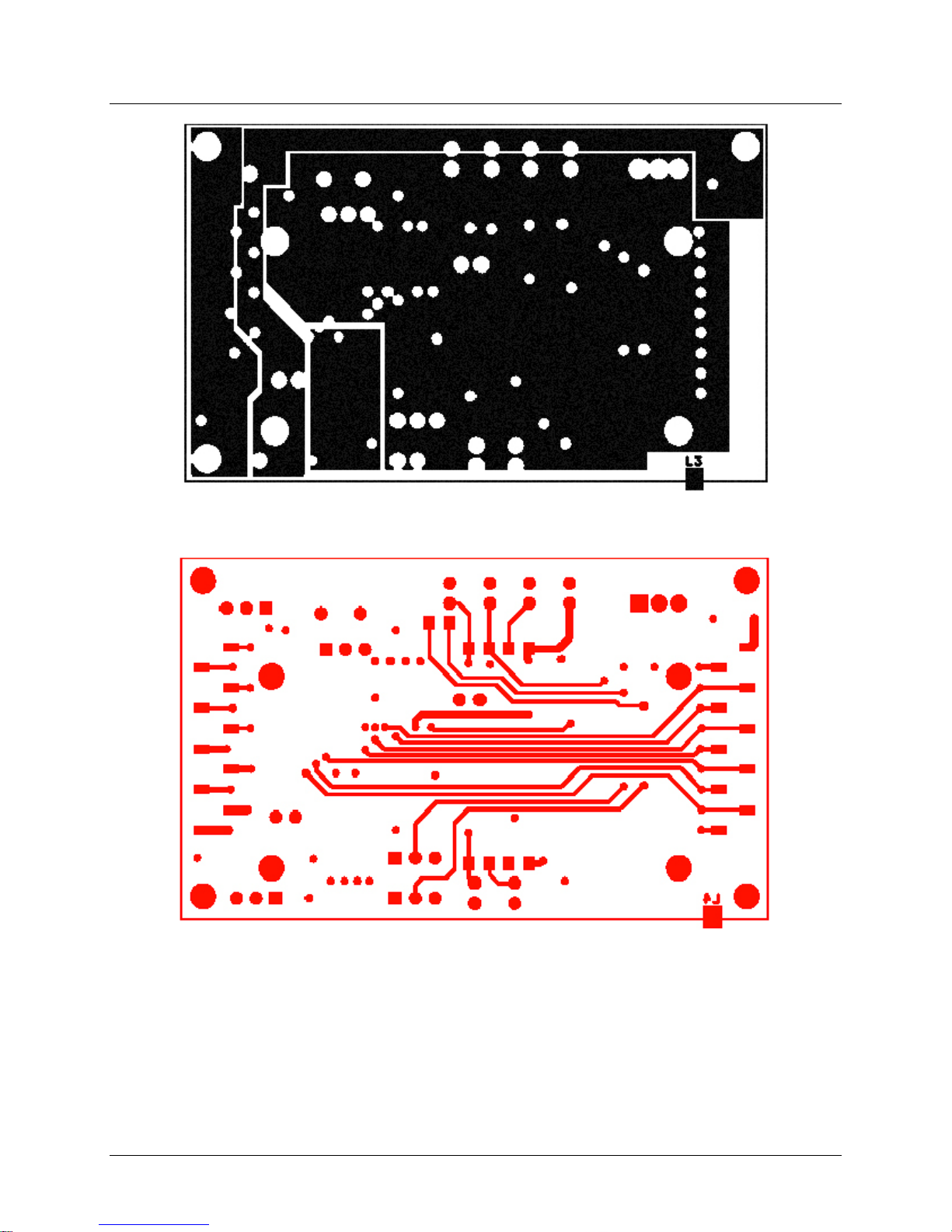
Figure 10: 73S8024C Middle Layer 2, Su p ply Plan e
Figure 11: 73S8024C Demo Board Bottom Signal Layer
Rev. 1.3 17
Page 18

73S 8024C Demo Board User Manual UM_8024C_061
6 Ordering Information
Table 9 lists the order num ber used to ide nti fy the 73S8024C Demo Board.
Table 9: Order Numbers and Packaging Marks
Part Description Ord er Number
73S8 02 4C 28-Pin SO Demo Boar d 73S8024C-DB
7 Related Documentation
The following 73S8024C documents ar e available fr om Terid i an Semiconductor Corporation:
73S8024C Data Sheet
73S8024C Demo Board User Manual (this document)
Teridian 73S8024C versus Philips TDA8024T Application Note
8 Contact Information
For m or e i nform ation about Teridian Semiconductor pr oducts or to check the availabilit y of the
73S8024C, contact us at:
644 0 Oak Canyon Road
Suite 100
Irvin e, CA 92618-5201
Telephone: (714) 508-8800
FAX: (714) 508-8878
Email: [email protected]
For a complete list of worldwide sa les offic es, g o to http://www.teridian.com.
18 Rev. 1.3
Page 19
UM_8024C_061 73S8024C Demo Board U ser Manual
1.2
8/23/2005
Added new logo.
Revision Hi story
Revision Date Description
1.0 6/8/2004 First publication.
1.1 8/2/2004 Min or correct ion s.
1.3 11/11/2009 Added Section 1.1, Package Contents.
Add ed Section 1 .2, Safety and E SD Not es.
Add ed Section 6 , Orderi ng Information.
Add ed Section 7 , R el ated Documentat i on.
Add ed Section 8 , C ontact Information.
Miscel lane ous editorial changes.
Rev. 1.3 19
Page 20

Mouser Electronics
Authorized Distributor
Click to View Pricing, Inventory, Delivery & Lifecycle Information:
Maxim Integrated:
73S8024C-DB
 Loading...