

Teridian 73S8023C User Manual

Simplifying System In tegrationTM
73S8023C
Demo Board User Manual
November 11 , 2009
Rev. 1.3
UM_8023C_027

73S 8023C Demo Board User Manual UM_8023C_027
© 20 09 Teridi an Semiconductor C or porati on. All rights r eserved .
Terid i an Semiconductor Corporation is a registered trademark of Teridi an Semiconductor Corporation.
Simplifying System Integ r ation i s a trademark of Teridian S emiconduct or C or poration .
All other trademarks ar e the property of thei r r espective owners.
Terid i an Semiconductor Corporation m akes n o warranty for the use of i ts p r oduct s, other than expr essly
contained in the Comp any’s warranty d etailed in the Terid ian S emiconductor Corporation st andar d Terms
and C onditions. The company assu mes no responsib i lity for any errors whi ch may appear in t his
document, reserves th e r i ght to change device s or sp ecifications detailed herein at any time withou t
notice and does n ot make any commitm ent to upd ate the information contained herein. Accordingl y, the
reader is cautioned to verify that t his document is current by comparing it to the latest version on
http://www.teridian .com or by checking with your sales represen tative.
Terid i an Semiconductor Corp., 64 40 Oak Canyon, Suite 100, Ir vine, CA 92618
TEL (714) 508-8800, FAX (714) 508-8877, http://www.teridian.com
2 Rev. 1.3

UM_8023C_027 73S8023C Demo Board U ser Manual
Table of Contents
1
Introduction ................................................................................................................................... 5
1.1 Packa ge Con tents.................................................................................................................... 5
1.2 Safety and ESD Not es ............................................................................................................. 5
2 Basic Connections ........................................................................................................................ 6
3 Hardware Description .................................................................................................................... 7
3.1 Demo Board C onnectors, Jump er s and Test Poin ts ................................................................. 7
3.2 Recommended Op er ating Conditions and Absolut e M aximum Rat ings ..................................... 9
3.3 73S 8023C Pin Descrip tion ....................................................................................................... 9
3.4 73S8023C Pinout ................................................................................................................... 11
4 Design Considerations ................................................................................................................ 12
4.1 Gener al Layout Rules ............................................................................................................ 12
4.2 Optimization for Compliance with EMV and NDS .................................................................... 12
5 73S8023C Demo Board Schematics, PCB Layouts and Bill of Materials .................................. 13
5.1 Schematic .............................................................................................................................. 13
5.2 Bill of Materials ...................................................................................................................... 14
5.3 PCB Layouts .......................................................................................................................... 15
6 Ordering Information ................................................................................................................... 18
7 Related Documentation ............................................................................................................... 18
8 Contact Information ..................................................................................................................... 18
Revision H istory .................................................................................................................................. 19
Rev. 1.3 3

73S 8023C Demo Board User Manual UM_8023C_027
Figures
Figure 1: 73S8023C Demo Board
Figure 2: 73S8023C Demo Board Basic Connections
Figure 3: 73S8023C Demo Board Connectors, Jumper s and Test Points
Figure 4: 73S8023C 32QFN Pinout (Top View)
Figure 5: 73S8023C Demo Board Electrical Schematic
Figure 6: 73S8023C Demo Board Top View
Figure 7: 73S8023C Demo Board Bottom View
Figur e 8: 73S8023C Demo B oar d Top S i gnal L ayer
Figure 9: 73S8023C Demo Board Middl e Layer 1, Grou nd Plane
Figure 10: 73S8023C Middle Layer 2, Supply Plane
Figure 11: 73S8023C D em o Board Bott om Sign al Layer
Tables
Table 1 : 73S8023C Dem o Board Con nect or , Jumper and Test P oi nts
Table 2: Recommended Operating Conditi ons
Table 3: Absolu te Maxim um Rat i ngs
Table 4: 73S8023C Card Interface Pins
Table 5: 73S8023C Misce llaneous Pi ns
Table 6: 73S8023C Power and Ground Pins
Table 7: 72S8023C Microcont r ol ler In terface Pins
Table 8: 73S8023C Demo Board Bill of Materials
Table 9: Order Numbers and Packagin g Marks
............................................................................................................ 5
.............................................................................. 6
................................................. 8
...................................................................................... 11
.......................................................................... 13
........................................................................................... 15
...................................................................................... 15
............................................................................... 16
........................................................... 16
.............................................................................. 17
........................................................................ 17
...................................................... 7
......................................................................................... 9
........................................................................................................ 9
................................................................................................... 9
................................................................................................. 10
.......................................................................................... 10
.................................................................................. 10
................................................................................... 14
...................................................................................... 18
4 Rev. 1.3
UM_8023C_027 73S8023C Demo Board U ser Manual
1 Introduction
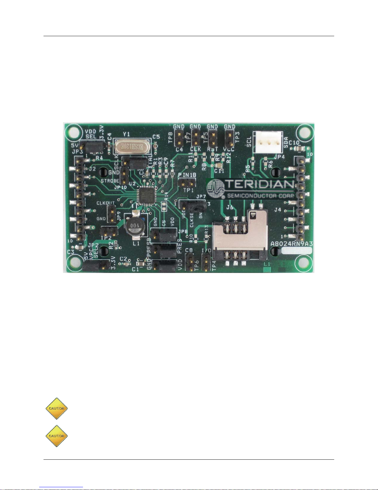
The 73S8023C Demo B oar d is a platform for evaluating the Teridian 73S8023C Smart Card Interface
device. The board incorporates the 73S8023C integrated circuit and has been design ed to operate either
as a st andal one platform ( to be used in conju nction with an extern al microcontroller) or as a daught er
card to be used in conjunction with the 73S1121F evaluation platform.
The board has been designed to comply with the EMV 2000 Specification, Version 4.0. 73S8023C Demo
Boards can easily be mod i fi ed to comply with NDS specifications by replacing a few external components
that are highlighted in this document.
Figure 1: 73S8023C Demo Boa rd
1.1 Package Contents
The 73S8023C Demo Board Kit includes:
• A 73S8023C Demo Board
• The following documents on CD:
• 73S8023C Data Sheet
• 73S8023C Demo Boar d Us er Ma n ual (this document)
• Application Note
1.2 Safety an d ES D Notes
Connecti ng live voltages to the 73S8023C Demo Board system will r esult in potentiall y hazard ous
voltages on the boards.
Extreme caution should be taken when handling the 73S8023C Demo Board after
connection to live voltages!
The 73S8023C Demo Board is ESD sensitive! ESD precautions should be taken when
handling this board!
Rev. 1.3 5
73S 8023C Demo Board User Manual UM_8023C_027
2 Basic Connections
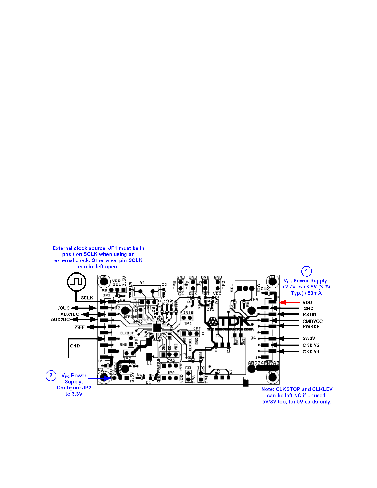
The basic connections to the demo boar d are d escribed below and shown in Figure 2.
1. Connect power supply: Apply 3.3 V to pin 10 of J4.
2. Control signals to the device can be connected through J2 and J4 (see Figure 2 and the Electrical
Schematic, Figure 5).
3. To set the clock frequency with an extern al cl ock source:
• Set JP1 to the SCLK setting.
• App l y clock source to pin 1 of J2.
• Apply 3. 3V (1) or GND (0) to C LKDIV1 and CLKDIV2 pins to set the desired clock r ate as f ol lows:
CLKDIV1 = CLKDIV2 = 0 clock frequency = SCLK/8
CLKDIV1 = 0, CLKDIV2 =1 clock frequency = SCLK/4
CLKDIV1 = 1, CLKDIV2 =0 clock frequency = SCLK
CLKDIV1 = CLKDIV2 = 1 clock frequency = SCLK/2
4. To set the clock frequency using crystal Y1:
• The crystal included on the demo boar d is 12 MHz.
• Set JP1 to XTAL position.
• Apply 3.3V (1) or GND (0) to CLKDIV1 and CLKDIV2 pins to set the desired clock rate as fol l ows:
CLKDIV1 = CLKDIV2 = 0 clock frequency = 1.5 MHz
CLKDIV1 = 0, CLKDIV2 =1 clock frequency = 3 MHz
CLKDIV1 = 1, CLKDIV2 =0 clock frequency = 12 MHz
CLKDIV1 = CLKDIV2 = 1 clock frequency = 6 MHz
Figure 2: 73S8023C Demo Board Basic Connections
6 Rev. 1.3
 Loading...