

Page 1
Page 2

XTS-FMC User
Manual
1 www.terasic.com
June 26, 2019
TABLE OF CONTENTS
Chapter 1 Introduction ................................................................................................................... 2
1.1 Features ............................................................................................................................................... 2
1.2 The Package Contents ......................................................................................................................... 3
1.3 Assemble XTS-FMC with FPGA Main board .................................................................................... 4
1.4 Getting Help ........................................................................................................................................ 5
Chapter 2 Board Specification ......................................................................................................... 6
2.1 Layout and Components ..................................................................................................................... 6
2.2 Block Diagram .................................................................................................................................... 7
2.3 Mechanical Specifications .................................................................................................................. 9
Chapter 3 Board Components ....................................................................................................... 10
3.1 FMC Expansion Connector ............................................................................................................... 10
3.2 Programmable Clock Generator........................................................................................................ 14
Chapter 4 Demonstrations ............................................................................................................. 15
4.1 XTS-FMC Loopback on the TR5 ..................................................................................................... 15
4.2 XTS-FMC Loopback on the Han Pilot Platform .............................................................................. 19
4.3 XTS-FMC SuperLite Loopback on the Han Pilot Platform.............................................................. 21
Appendix
24
Revision History ..................................................................................................................................... 24
Page 3

XTS-FMC User
Manual
2 www.terasic.com
June 26, 2019
Chapter 1
Introduction
The XTS-FMC daughter card is designed to convert FPGA transceiver channels to SMA connectors
through a FPGA Mezzanine Card(FMC) interface. It is intended to allow users to evaluate the
performance of transceiver-based host boards with FMC interface specifically the Stratix, Arria and
Cyclone FPGA with integrated transceivers. Through the SMA connectors, the FPGA transceiver
signals can be easily connected to measurement instruments as well as allowing gigabit data rate
communication between multiple FPGA boards. In addition, there is a clock generator (CDCM6208)
that can output the various reference clock for different applications to the transceiver bank of the
FPGA through the FMC connector.
The XTS-FMC daughter card is the ideal platform to allow users to prototype and test their
high-speed interfaces quickly and easily in support of transceiver performance for jitter, protocol
compliance, and equalization.
11..1
1
FFeeaattuurreess
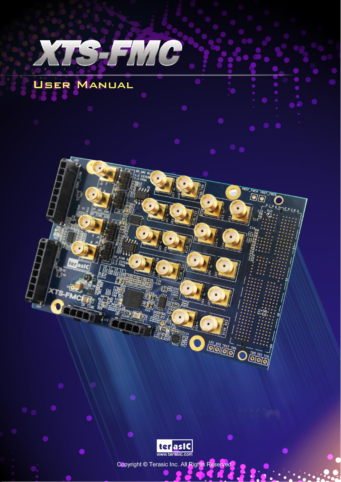
Figure 1-1 shows the photo of the XTS-FMC card. The important functions of the XTS-FMC card
are listed below:
• Convert FPGA transceiver channels to SMA connectors through FMC connector
• Support maximum 4 transceiver channels (Depend on the FPGA host board)
• SMA connectors for external clock input
• Programmable clock generator for reference clock input
Page 4
XTS-FMC User
Manual
3 www.terasic.com
June 26, 2019
Figure 1-1 The XTS-FMC Card.
11..2
2
TThhee PPaacckkaaggee CCoonntteennttss
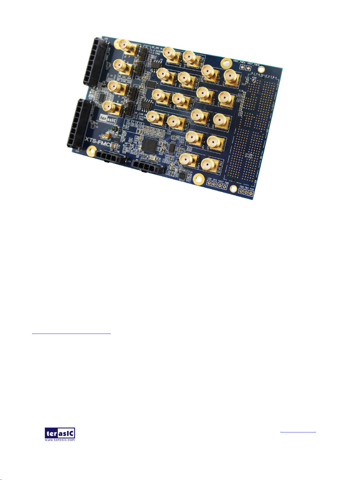
The XTS-FMC kit comes with the following items (see Figure 1-2):
1. XTS-FMC Daughter Card
2. Screw & Copper Pillar Package
3. CD Download Guide
The system CD contains technical documents of the XTS-FMC card, which include component
datasheets, demonstrations, schematic and user manual. Users can download the CD from the link
below:
http://xts-fmc.terasic.com/cd
Page 5
XTS-FMC User
Manual
4 www.terasic.com
June 26, 2019
Figure 1-2 The contents of the XTS-FMC card.
11..3
3
AAsssseemmbbllee XXTTSS--FFMMCC wwiitthh FFPPGGAA MMaaiinn bbooaarrdd
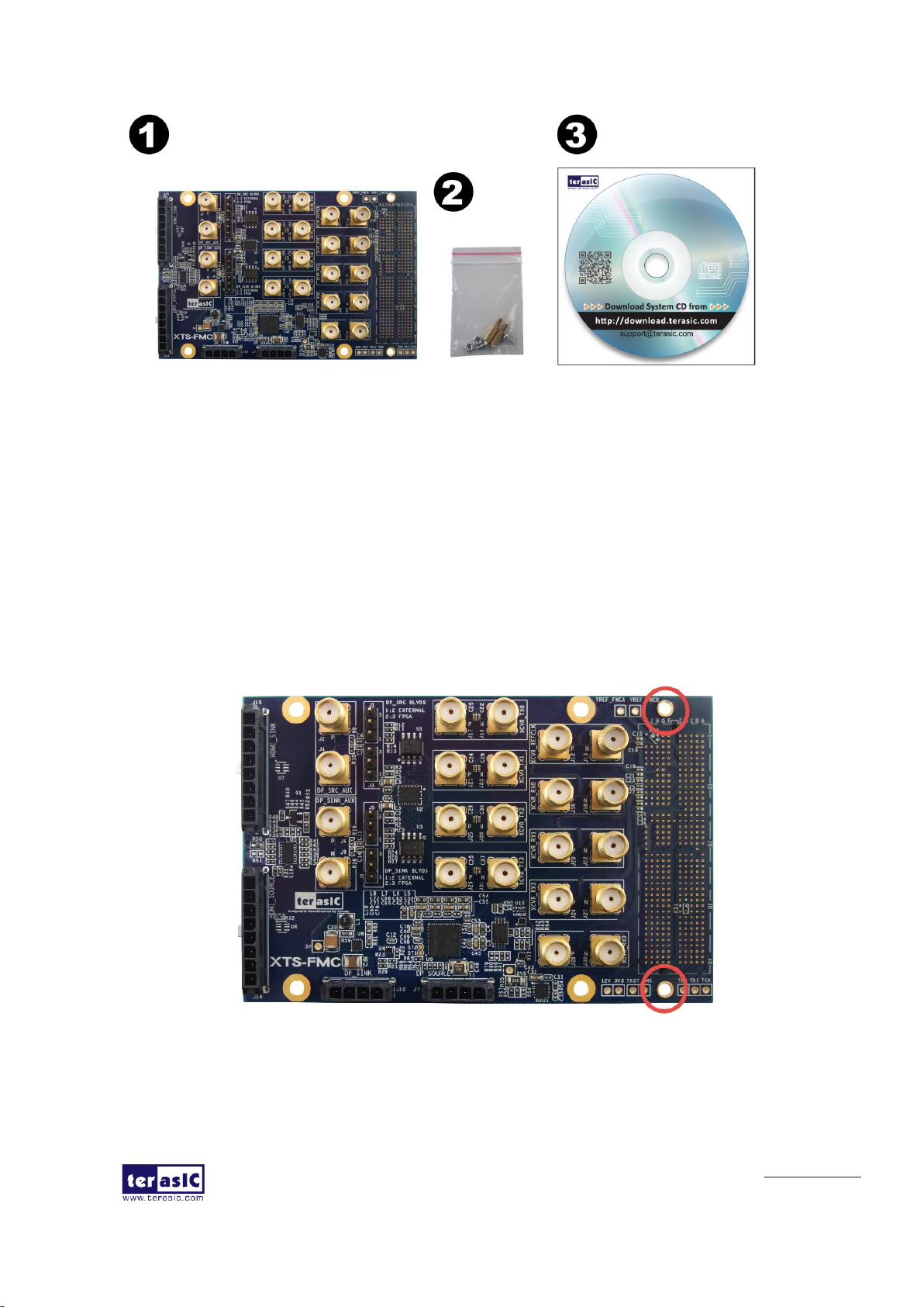
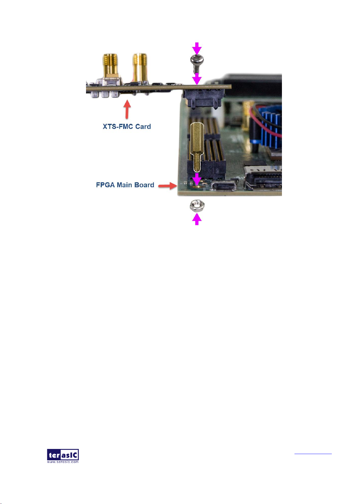
In order to make the XTS-FMC daughter card and the FMC connector on the FMC card with more
secure hookup, the FMC side of the XTS-FMC daughter card has reserved two screw holes, as
shown in Figure 1-3. Users can use the screws, copper pillars, and nuts that come with the XTSFMC, to secure the XTS-FMC on the FPGA main board, as shown in Figure 1-4. Because
transceiver is mostly used for high-speed transmission applications, we strongly recommend that
users use the screws to secure the connection between the FPGA main board and the XTS-FMC
card.
Figure 1-3 The two screw holes on XTS-FMC card.
Page 6
XTS-FMC User
Manual
5 www.terasic.com
June 26, 2019
Figure 1-4 Secure the XTS-FMC on the FPGA main board
11..4
4
GGeettttiinngg HHeellpp
Here are the addresses where you can get help if you encounter any problems:
Terasic Technologies
9F., No.176, Sec.2, Gongdao 5th Rd, East Dist, Hsinchu City, 30070. Taiwan
Email: support@terasic.com
Tel.: +886-3-575-0880
Website: xts-fmc.terasic.com
Page 7
XTS-FMC User
Manual
6 www.terasic.com
June 26, 2019
Chapter 2
Board Specification
This chapter describes the architecture of the XTS card including block diagram and components.
22..1
1
LLaayyoouutt aanndd CCoommppoonneennttss
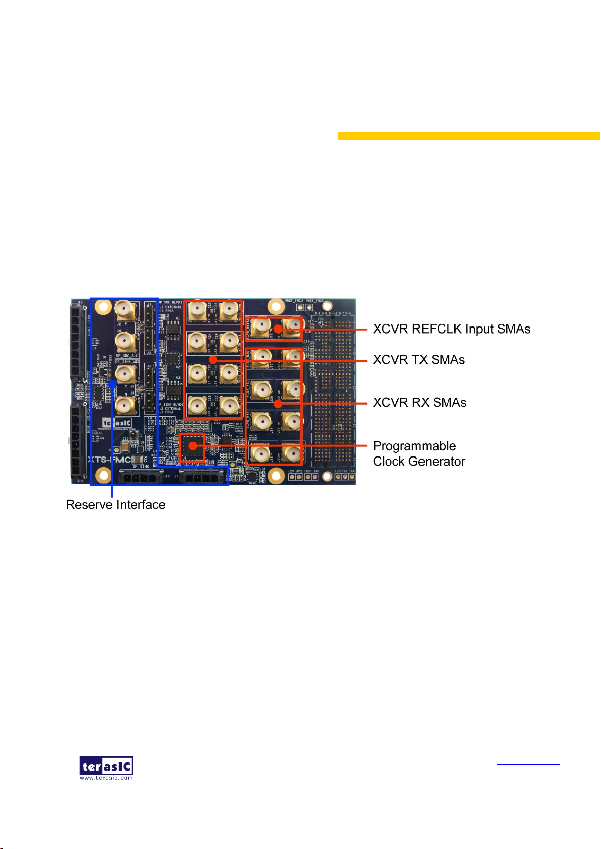
The picture of the XTS-FMC card is shown in Figure 2-1 and Figure 2-2. It depicts the layout of
the board and indicates the locations of the connectors and key components.
Note: The interface labeled with the blue block in Figure 2-1 is the reserve interface and can be
ignored.
Figure 2-1 Mechanical Layout of the XTS-FMC card
Page 8
XTS-FMC User
Manual
7 www.terasic.com
June 26, 2019
Figure 2-2 Mechanical Layout of the XTS-FMC card
The following components are provided on the XTS-FMC card:
• FMC expansion connector (J11)
• TX SMAs (J17/J19,J21/J23,J25/J26,J29/J31)
• RX SMAs (J16/J18,J20/J22,J24/J27,J28/J30)
• XCVR reference input SMAs (J12/J13)
22..2
2
BBlloocckk DDiiaaggrraamm
Figure 2-3 is the block diagram of the XTS-FMC card.
Page 9

XTS-FMC User
Manual
8 www.terasic.com
June 26, 2019
Figure 2-3 Block diagram of the XTS-FMC card
Page 10

XTS-FMC User
Manual
9 www.terasic.com
June 26, 2019
22..3
3
MMeecchhaanniiccaall SSppeecciiffiiccaattiioonnss
Figure 2-3 is the mechanical layout of the XTS-FMC board.
Figure 2-4 The mechanical layout of the XTS-FMC card
Page 11

XTS-FMC User
Manual
10
www.terasic.com
June 26, 2019
Chapter 3
Board Components
This chapter will describe the detailed information of the components, connector interface, and the
pin mappings on the XTS-FMC card.
33..1
1
FFMMCC EExxppaannssiioonn CCoonnnneeccttoorr
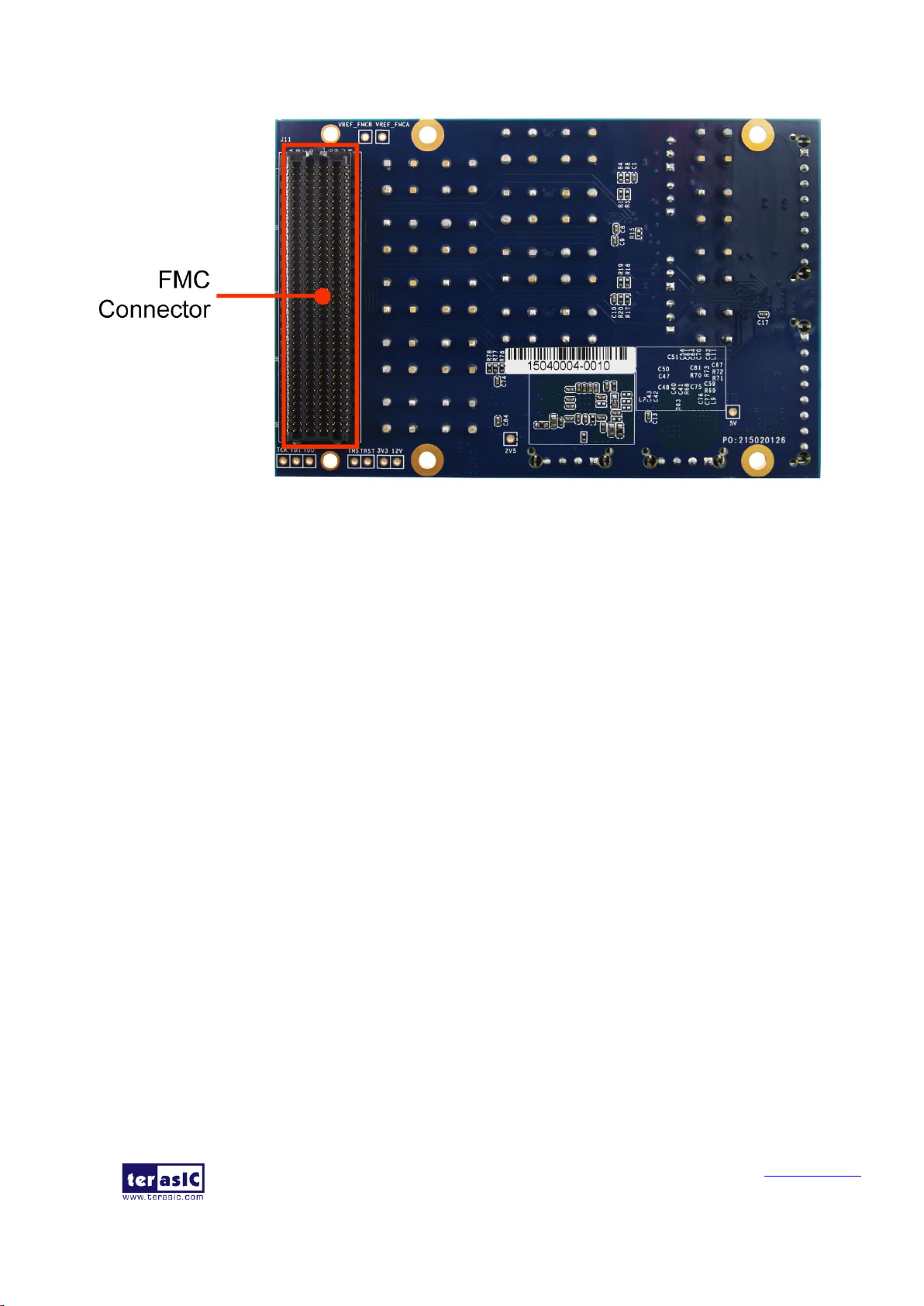
The XTS-FMC card contains an FPGA Mezzanine Card (FMC) connector. All the other interfaces
on the XTS-FMC card are connected to the FMC connector. Figure 3-1, Figure 3-2, Figure 3-3,
and Figure 3-4 show the pin-outs of the FMC connector and Table 3-1 lists the description of each
signals corresponding to the FMC connector.
Figure 3-1 Signal names of XTS-FMC connector part 1
Page 12

XTS-FMC User
Manual
11
www.terasic.com
June 26, 2019
Figure 3-2 Signal names of XTS-FMC connector part 2
Figure 3-3 Signal names of XTS-FMC connector part 3
Page 13

XTS-FMC User
Manual
12
www.terasic.com
June 26, 2019
Figure 3-4 Signal names of XTS-FMC connector part 4
Table 3-1 FMC Pin Assignments
Signal Name
FMC Pin
No.
Direction
I/O Standard
Description
XCVR_TX0_p
PIN_C2
Output
1.4-V PCML
SMA Transceiver Output Port0,
connected to J17(SMA)
XCVR_TX0_n
PIN_C3
Output
1.4-V PCML
SMA Transceiver Output Port0,
connected to J19(SMA)
XCVR_TX1_p
PIN_A22
Output
1.4-V PCML
SMA Transceiver Output Port1,
connected to J21(SMA)
XCVR_TX1_n
PIN_A23
Output
1.4-V PCML
SMA Transceiver Output Port1,
connected to J23(SMA)
Page 14

XTS-FMC User
Manual
13
www.terasic.com
June 26, 2019
XCVR_TX2_p
PIN_A26
Output
1.4-V PCML
SMA Transceiver Output Port2,
connected to J25(SMA)
XCVR_TX2_n
PIN_A27
Output
1.4-V PCML
SMA Transceiver Output Port2,
connected to J26(SMA)
XCVR_TX3_p
PIN_A30
Output
1.4-V PCML
SMA Transceiver Output Port3,
connected to J29(SMA)
XCVR_TX3_n
PIN_A31
Output
1.4-V PCML
SMA Transceiver Output Port3,
connected to J31(SMA)
XCVR_RX0_p
PIN_C6
Input
1.4-V PCML
SMA Transceiver Input Port0,
connected to J16(SMA)
XCVR_RX0_n
PIN_C7
Input
1.4-V PCML
SMA Transceiver Input Port0,
connected to J18(SMA)
XCVR_RX1_p
PIN_A2
Input
1.4-V PCML
SMA Transceiver Input Port1,
connected to J20(SMA)
XCVR_RX1_n
PIN_A3
Input
1.4-V PCML
SMA Transceiver Input Port1,
connected to J22(SMA)
XCVR_RX2_p
PIN_A6
Input
1.4-V PCML
SMA Transceiver Input Port2,
connected to J24(SMA)
XCVR_RX2_n
PIN_A7
Input
1.4-V PCML
SMA Transceiver Input Port2,
connected to J27(SMA)
XCVR_RX3_p
PIN_A10
Input
1.4-V PCML
SMA Transceiver Input Port3,
connected to J28(SMA)
XCVR_RX3_n
PIN_A11
Input
1.4-V PCML
SMA Transceiver Input Port3,
connected to J30(SMA)
XCVR_REFCLK0_p
PIN_D4
Input
LVDS
External reference clock input,
connected to J12(SMA)
XCVR_REFCLK0_n
PIN_D5
Input
LVDS
External reference clock input,
connected to J13(SMA)
XCVR_REFCLK1_p
PIN_B20
Input
LVDS
External reference clock input,
connected to the clock generator
CDCM6208.
XCVR_REFCLK1_n
PIN_B21
Input
LVDS
External reference clock input,
connected to the clock generator
CDCM6208.
FMC_I2C_SDA
PIN_C31
Inout
VCCADJ
I2C data bus for the clock generator
CDCM6208
FMC_I2C_SCL
PIN_C30
Ouput
VCCADJ
I2C clock bus for the clock generator
CDCM6208
Page 15

XTS-FMC User
Manual
14
www.terasic.com
June 26, 2019
33..2
2
PPrrooggrraammmmaabbllee CClloocckk GGeenneerraattoorr
The XTS-FMC card provides a programmable clock generator: CDMC6208. This clock generator
provides a variety of frequencies which can have different formats to the FPGA's transceiver bank
for different applications as reference clock. The user can modify the output frequency of
DMC6208 from the FPGA through the I2C interface. The I2C address of this device is 7'b1010100.
Figure 3-5 Block diagram of the FMC connector and the CDCM208
Page 16

XTS-FMC User
Manual
15
www.terasic.com
June 26, 2019
Chapter 4
Demonstrations
This chapter illustrates the transcevier loopback reference design for the XTS-FMC card.
44..1
1
XXTTSS--FFMMCC LLooooppbbaacckk oonn tthhee TTRR55
The transceiver test code is used to verify 4 transceiver channels of the FMC connector through the
XTS-FMC card and SMA cables. The transceiver channels are verified with PRBS31 test pattern
and with the data rates. For 5SGXEA7N2F45C2 Device of the TR5 board, the data rate of the
transceiver channel on the FMC connector runs at 12.5G bps.
◼ Required Equipments
To enable an external loopback of transceiver channels, the following fixtures are required:
⚫ TR5 board and XTS-FMC card.
⚫ 8 SMA cables for loopback the TX and RX port on the XTS-FMC card.
◼ Demonstration Setups
The transceiver test code is available in the folder System CD\Demonstrations\TR5\demo_batch.
Here are the procedures to perform transceiver channel test:
1. Use the SMA cables to connect the TX ports and the RX ports on the XTS-FMC card to
implement the loopback function (See Figure 4-1, Figure 4-2). There are four channels in total,
note the difference between positive and negative ports.
Figure 4-1 SMA loopback setup
Page 17

XTS-FMC User
Manual
16
www.terasic.com
June 26, 2019
2. Connect the XTS-FMC card to the FMC D or FMC A connector of the TR5 board. Make sure
the FMC connector between the two boards is locked with copper posts and screws (See
section 1.3).
Figure 4-2 The Connections between the XTS-FMC card and TR5 board
3. Connect your TR5 board to your PC with a mini USB cable.
4. Connect Power to the TR5 board.
5. Copy the demo_batch folder (from System CD) to your local disk.
6. Power on the TR5 board.
7. Execute 'test.bat" in the demo_batch folder under your local disk.
8. The batch file will download .sof and .elf files, and start the test. The Nios-Terminal as shown
in Figure 4-3 will appear and choose “0” to test all the transceiver loopback test.
Page 18

XTS-FMC User
Manual
17
www.terasic.com
June 26, 2019
Figure 4-3 Choose the Test function
9. Then enter how many seconds you want to test the transmission (See Figure 4-4). For example,
enter “60” for test 60 second.
Page 19

XTS-FMC User
Manual
18
www.terasic.com
June 26, 2019
Figure 4-4 Choose test duration
10. The test result will be displayed after the test time has elapsed (See Figure 4-5). It should be
noted that this test code will test all the transceivers of the FMC A and FMC D connectors on
the TR5 board (8 pairs of transceivers for each connector). Since XTS-FMC card can only test
4 pairs of transceivers. So the test result will only show the first four transceivers (0~3) of
FMC A or FMC D are PASS or NG. Other transceiver test results can be ignored.
Figure 4-5 The test result of the transceiver loopback
Page 20

XTS-FMC User
Manual
19
www.terasic.com
June 26, 2019
44..2
2
XXTTSS--FFMMCC LLooooppbbaacckk oonn tthhee HHaann PPiilloott PPllaattffoorrmm
This section describes the use of the XTS-FMC card to test the FPGA's transceiver loopback on the
HAN pilot platform. The basic operation is roughly the same as section 4.1, except that the FPGA
board is replaced. The following is a detailed test procedure.
◼ Required Equipments
To enable an external loopback of transceiver channels, the following fixtures are required:
⚫ HAN Pilot Platform and XTS-FMC card.
⚫ 8 SMA cables for loopback the TX and RX ports on the XTS-FMC card.
◼ Demonstration Setups
The transceiver test code is available in the folder System CD\Demonstrations\HAN\XCVT
loopback. Here are the procedures to perform transceiver channel test:
1. Use the SMA cables to connect the TX ports and the RX ports on the XTS-FMC card to
implement the loopback function (See Figure 4-6).
2. Connect the XTS-FMC card to the FMC connector of the HAN Pilot Platform board. Make
sure the FMC connector between the two boards is locked with copper posts and screws (See
section 1.3).
Figure 4-6 The Connections between the XTS-FMC and HAN Pilot Platform board
Page 21

XTS-FMC User
Manual
20
www.terasic.com
June 26, 2019
3. Connect your HAN board to your PC with a mini USB cable.
4. Connect Power to the HAN Pilot Platform board.
5. Copy the demo_batch folder (from System CD) to your local disk.
6. Power on the HAN Pilot Platform board.
7. Execute 'test.bat" in the demo_batch folder under your local disk.
8. The batch file will download .sof and .elf files, and start the test in the Nios-Terminal as shown
in Figure 4-7. When the menu option appears, you can choose 0 for starting test. The program
will automatically start the test and report the test results every five seconds until the user
closes the window (see Figure 4-8).
Figure 4-7 The test program
Page 22

XTS-FMC User
Manual
21
www.terasic.com
June 26, 2019
Figure 4-8 Test result
44..3
3
XXTTSS--FFMMCC SSuuppeerrLLiittee LLooooppbbaacckk oonn tthhee HHaann PPiilloott PPllaattffoorrmm
This section also describes the use of the XTS-FMC card to test the FPGA's RX/TX transceiver
loopback on the HAN pilot platform, this XTS-FMC SuperLite Loopback demonstration is created
based on Intel High Speed Transceiver Demo Designs, we ported it to HAN Pilot Platform
combined with XTS-FMC card, the data rate of the transceiver channel on the FMC connector runs
at 12.5Gbps.
User can refer to A10GX_SIBoard_SuperliteII_V3_4_lanes_10Gbps_QSFP+.pdf document
in the folder System CD\Demonstrations\HAN\A10GX_SIBoard_SuperliteII_V3_4_lanes_10Gbp
s_QSFP+.pdf for detail description.
◼ Demonstration Setups
The transceiver test code is available in the folder System CD\Demonstrations\HAN\
SuperLite Loopback\demo_batch. Here are the procedures to perform transceiver channel test:
1. Use the SMA cables to connect the TX ports and the RX ports on the XTS-FMC card to
implement the loopback function (See Figure 4-9).
2. Connect the XTS-FMC card to the FMC connector of the HAN Pilot Platform board. Make sure
the FMC connector between the two boards is locked with copper posts and screws (See section
1.3).
Page 23

XTS-FMC User
Manual
22
www.terasic.com
June 26, 2019
Figure 4-9 The Connections between the XTS-FMC and HAN Pilot Platform board
3. Connect your HAN board to your PC with a mini USB cable.
4. Connect Power to the HAN Pilot Platform board.
5. Copy the demo_batch folder (from System CD) to your local disk.
6. Power on the HAN Pilot Platform board.
7. Execute 'test.bat" in the demo_batch folder under your local disk.
8. The batch file will download .sof and .elf files, and start the test in the Nios-Terminal as shown
in Figure 4-10. When the menu option appears, use can choose C to start the test, if the
Nios-Terminal shows ‘0’ all the time, it means that the loopback test is passed without error.
Page 24

XTS-FMC User
Manual
23
www.terasic.com
June 26, 2019
Figure 4-10 Start the test in the Nios-Terminal
9. The signal XCVR quality depends on the device (such as scope, SMA cables) which is
connected to the XCVR REFCLK Input SMA connector, user needs to modify the PMA
parameters. Choose the action 3 (Select Channel to Control) in the Nios-Terminal to change
channel, then choose action 4 (Show/Control Transceiver PMA Settings on Links) to modify the
PMA parameters. Based on our actual experiment, we provided a group of PMA parameters as
shown in Table 4-1, user can modify the PMA parameters by referring the values in .
Table 4-1 PMA parameters based on our actual experiment
VOD
29
PostTap
-9
PreTap
-1
other
Default
Page 25

XTS-FMC User
Manual
24
www.terasic.com
June 26, 2019
Appendix
RReevviissiioonn HHiissttoorryy
Version
Change Log
V1.0
Initial Version (Preliminary)
V1.1
Add section 2.3
V1.2
Add section 4.3
Copyright © Terasic Inc. All rights reserved.
 Loading...