

Page 1
1
Page 2

1
CONTENTS
CONTENTSCONTENTS
CONTENTS
CHAPTER 1
CHAPTER 1CHAPTER 1
CHAPTER 1
INTRODUCTION OF THE
INTRODUCTION OF THE INTRODUCTION OF THE
INTRODUCTION OF THE VEEK
VEEKVEEK
VEEK----MT
MTMT
MT----C5SOC
C5SOCC5SOC
C5SOC
................................
................................................................
................................................................
................................................................
.................................... 1111
1.1
Cyclone V SX SoC Development Board ............................................................................................. 2
1.2
Setup License for Terasic Multi-touch IP ............................................................................................ 6
1.3
Getting Help ........................................................................................................................................ 7
CHAPTER 2
CHAPTER 2CHAPTER 2
CHAPTER 2
ARCHITECTURE
ARCHITECTUREARCHITECTURE
ARCHITECTURE
................................
................................................................
................................................................
................................................................
................................................................
................................................................
............................................
........................
............ 8888
2.1 Layout and Components ............................................................................................................................. 8
2.2 Block Diagram of the VEEK-MT-C5SOC ................................................................................................. 9
CHAPTER 3
CHAPTER 3CHAPTER 3
CHAPTER 3
USING VEEK
USING VEEKUSING VEEK
USING VEEK----MT
MTMT
MT----C5SOC
C5SOCC5SOC
C5SOC
................................
................................................................
................................................................
................................................................
............................................................
........................................................
............................ 10
1010
10
3.1 Using the Cyclone® V SX SoC FPGA .................................................................................................... 10
3.2 Using the 7” LCD Capacitive Touch Screen ............................................................................................ 10
3.3 Using 5-megapixel Digital Image Sensor ................................................................................................. 12
3.4 Using the Digital Accelerometer .............................................................................................................. 13
3.5 Using the Ambient Light Sensor .............................................................................................................. 14
3.6 Using Terasic Multi-touch IP.................................................................................................................... 14
CHAPTER 4
CHAPTER 4CHAPTER 4
CHAPTER 4
VEEK
VEEKVEEK
VEEK----MT
MTMT
MT----C5SOC DEMONSTRATION
C5SOC DEMONSTRATIONC5SOC DEMONSTRATION
C5SOC DEMONSTRATIONSSSS
................................
................................................................
................................................................
................................................................
......................................
............
...... 17
1717
17
4.1 System Requirements ............................................................................................................................... 17
4.2 Painter Demonstration .............................................................................................................................. 17
4.3 Camera Application .................................................................................................................................. 21
4.4 Digital Accelerometer Demonstration ...................................................................................................... 25
CHAPTER 5
CHAPTER 5CHAPTER 5
CHAPTER 5
APPENDIX
APPENDIXAPPENDIX
APPENDIX
................................
................................................................
................................................................
................................................................
................................................................
................................................................
...................................................
......................................
................... 28
2828
28
5.1 Revision History ....................................................................................................................................... 28
5.2 Copyright Statement ................................................................................................................................. 28
Page 3

1
Chapter 1
Chapter 1Chapter 1
Chapter 1
Introduction
IntroductionIntroduction
Introduction of the
of the of the
of the VEEK
VEEKVEEK
VEEK----MT
MTMT
MT----C5SOC
C5SOCC5SOC
C5SOC
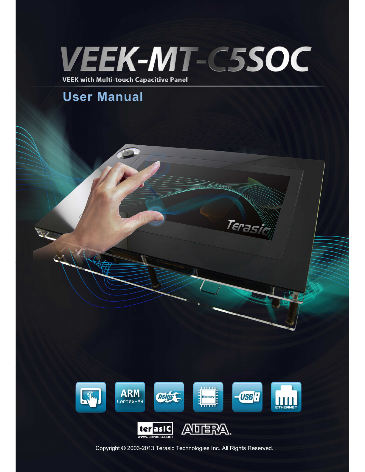
The Video and Embedded Evaluation Kit - Multi-touch on Cyclone® V SOC Development Board
(VEEK-MT-C5SOC) is a comprehensive design environment with everything embedded developers
need to create processing-based systems. VEEK-MT-C5SOC delivers an integrated platform that
includes hardware, design tools, intellectual property (IP) and reference designs for developing
embedded software and hardware platform in a wide range of applications. The fully integrated kit
allows developers to rapidly customize their processor and IP to best suit their specific application.
The VEEK-MT-C5SOC features the Altera Cyclone® V SoC development board targeting the
Altera Cyclone® V SX SoC FPGA, as well as a capacitive LCD multimedia color touch panel
which natively supports multi-touch gestures. A 5-megapixel digital image sensor, ambient light
sensor, and 3-axis accelerometer make up the rich feature-set.
The all-in-one embedded solution offered on the VEEK-MT-C5SOC, in combination of the LCD
touch panel and digital image module, provides embedded developers the ideal platform for
multimedia applications with unparallel processing performance. Developers can benefit from the
use of FPGA-based embedded processing system such as mitigating design risk and obsolescence,
design reuse, reducing bill of material (BOM) costs by integrating powerful graphics engines within
the FPGA, and lower cost.
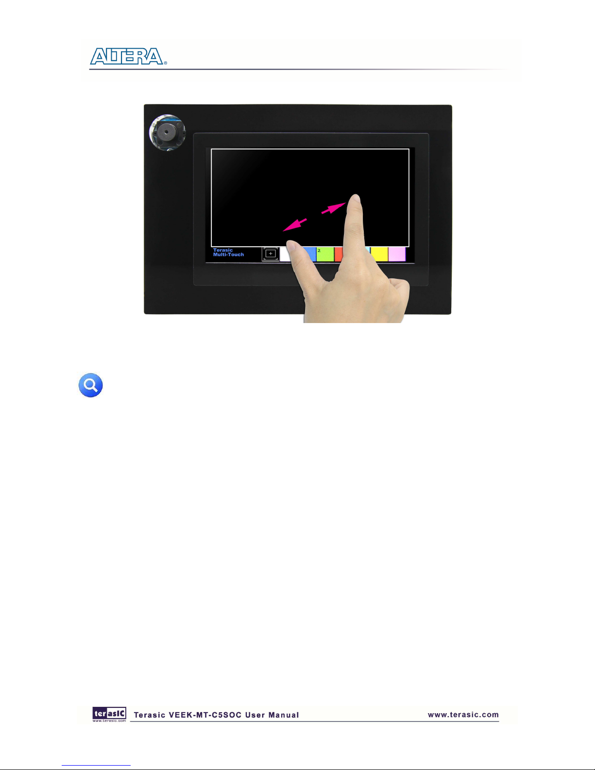
Figure 1-1 shows a photograph of VEEK-MT-C5SOC.
Page 4

2
Figure 1-1 The VEEK-MT-C5SOC board overview
The key features of the board are listed below:
11..1
1
CCyycclloonnee VV SSXX SSooCC DDeevveellooppmmeenntt
BBooaarrd
d
•••• Cyclone V SX SoC—5CSXFC6D6F31C6N
o 110K LEs, 41509 ALMs
o 5140 M10K memory blocks
o 224 18x18 Multiplier
o 6 FPGA PLLs and 3 HPS PLLs.
•••• Configuration Sources
o Active Serial (AS) x1 or x4 configuration (EPCQ256SI16N)
o MAX® V CPLD (5M2210ZF256I5N) in a 256-pin FBGA package as the System
Controller
o Flash fast passive parallel (FPP) configuration
o MAX II CPLD (EPM570GM100) as part of the embedded USB-BlasterTM II for
use with the Quartus® II Programmer
•••• Memory Devices
o One 1,024-Mbyte (MB) HPS DDR3 SDRAM with error correction code (ECC)
support
o One 1,024-MB FPGA DDR3 SDRAM
o One 256-Megabit (Mb) quad serial peripheral interface (QSPI) flash
o One 512-Mb CFI flash
o One 32-Kb I2
Page 5

3
o C serial electrically erasable PROM (EEPROM)
o One Micro SD flash memory card
•••• Switches and Indicators
o LEDs and displays
o Eight user LEDs
o One configuration load LED
o One configuration done LED
o One error LED
o Three configuration select LEDs
o Four on-board USB-Blaster II status LEDs
o One HSMC interface LED
o Two UART data transmit and receive LEDs
o One power on LED
o One two-line character LCD display
o Push buttons
o One CPU reset push button
o One MAX V reset push button
o One program select push button
o One program configuration push button
o Six general user push buttons
o DIP switches
o One MAX V CPLD System Controller control switch
o One JTAG chain control DIP switch
o One mode select DIP switch
o One general user DIP switch
•••• On-board Clocking Circuitry
o Si570, Si571, and Si5338 programmable oscillators
o 25-MHz, 50-MHz,100-MHz, 125-MHz, 148.50-MHz, and 156.25-MHz
•••• Oscillators
o SMA input (LVCMOS)
•••• Communication Ports
o One PCI Express x4 Gen1 socket
o One universal HSMC port
o One USB 2.0 on-the-go (OTG) port
o One Gigabit Ethernet port
o Dual 10/100 Ethernet ports
o One SDI port (option for SMA connection)
o One controller area network (CAN) port
o One RS-232 UART (through the mini-USB port)
o One real-time clock
Page 6
4
•••• Power
o 14–20-V (laptop) DC input
•••• Mechanical
o 5.2" × 8.2" rectangular form factor
Capacitive LCD Touch Screen
•••• Equipped with an 7-inch Amorphous-TFT-LCD (Thin Film Transistor Liquid
Crystal Display) module
•••• Module composed of LED backlight
•••• Support 24-bit parallel RGB interface
•••• Converting the X/Y coordination of touch point to its corresponding digital data via the Touch
controller.
Table 1-1 shows the general physical specifications of the touch screen (Note*).
Table 1-1 General physical specifications of the LCD
Item Specification Unit
LCD size 7-inch (Diagonal) Resolution 800 x3(RGB) x 480 dot
Dot pitch 0.1926(H) x0.1790 (V) mm
Active area 154.08 (H) x 85.92 (V) mm
Module size 164.9(H) x 100.0(V) x 5.7(D) mm
Surface treatment Glare Color arrangement RGB-stripe Interface Digital -
5-Megapixel Digital Image Sensor
•••• Superior low-light performance
•••• High frame rate
•••• Global reset release, which starts the exposure of all rows simultaneously
•••• Bulb exposure mode, for arbitrary exposure times
•••• Snapshot-mode to take frames on demand
•••• Horizontal and vertical mirror image
•••• Column and row skip modes to reduce image size without reducing field-of-view
•••• Column and row binning modes to improve image quality when resizing
•••• Simple two-wire serial interface
•••• Programmable controls: gain, frame rate, frame size, exposure
Page 7

5
Table 1-2 shows the key parameters of the CMOS sensor (Note*).
Table 1-2 Key performance parameters of the CMOS sensor
Parameter Value
Active Pixels 2592Hx1944V
Pixel size 2.2umx2.2um
Color filter array RGB Bayer pattern
Shutter type Global reset release(GRR)
Maximum data rate/master clock 96Mp/s at 96MHz
Frame rate
Full resolution Programmable up to 15 fps
VGA mode Programmable up to 70 fps
ADC resolution 12-bit
Responsivity 1.4V/lux-sec(550nm)
Pixel dynamic range 70.1dB
SNRMAX 38.1dB
Supply Voltage
Power 3.3V
I/O 1.7V~~~~3.1V
DDiiggiittaall AAcccceelleerroommeetteerr
o Up to 13-bit resolution at +/- 16g
o SPI (3- and 4-wire) digital interface
o Flexible interrupts modes
AAmmbbiieenntt LLiigghhtt SSeennssoorr
o Approximates human-eye response
o Precise luminance measurement under diverse lighting conditions
o Programmable interrupt function with user-defined upper and lower threshold settings
o 16-bit digital output with I2C fast-mode at 400 kHz
o Programmable analog gain and integration time
o 50/60-Hz lighting ripple rejection
Note: for more detailed information of the LCD touch panel and CMOS sensor module,
please refer to their datasheets respectively.
Page 8
6
11..2
2
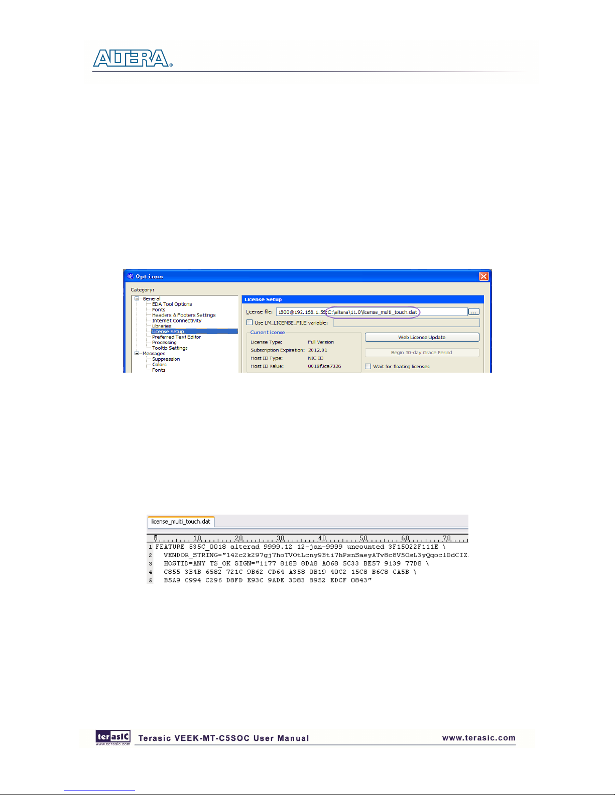
SSeettuupp LLiicceennssee ffoorr TTeerraassiicc MMuullttii--ttoouucchh IIPP
To utilize the multi-touch panel in a Quartus II project, a Terasic Multi-Touch IP is required. After a
license file for Quartus II is installed, there is one more license file needed to implement Terasic’s
Multi-touch IP. Error messages will be displayed if the license file is not added before compiling
projects using Terasic Multi-touch IP. The license file is located at:
VEEK-MT-C5SOC System CD\License\license_multi_touch.dat
There are two ways to install the License. The first one is to add the license file
(license_multi_touch.dat) to the licensed file listed in Quartus II, as shown in Figure 1-2.
Figure 1-2 License Setup
The second way is to add license content to the existing license file. The procedures are listed
below:
Use Notepad or other text editing software to open the file license_multi_touch.dat.
1. The license contains the FEATURE lines required to license the IP Cores as shown in Figure
1-3.
Figure 1-3 Content of license_multi_touch.dat
2. Open your Quartus II license.dat file in a text editor.
3. Copy everything under license_multi_touch.dat and paste it at the end of your Quartus II
license file. (Note: Do not delete any FEATURE lines from the Quartus II license file. Doing
so will result in an unusable license file.) .
4. Save the Quartus II license file.
Page 9

7
11..3
3
GGeettttiinngg HHeellpp
Here is the contact information should you encounter any problem:
•••• Terasic Technologies
•••• Tel: +886-3-575-0880
•••• Email: support@terasic.com
Page 10

8
Chapter 2
Chapter 2Chapter 2
Chapter 2
Architecture
ArchitectureArchitecture
Architecture
This chapter describes the architecture of the VEEK-MT-C5SOC including block diagram and
components.
22..1
1
LLaayyoouutt aanndd CCoommppoonneennttss
The picture of the VEEK-MT-C5SOC is shown in Figure 2-1 and Figure 2-2. It depicts the layout
of the board and indicates the locations of the connectors and key components.
Figure 2-1 VEEK-MT-C5SOC PCB and Component Diagram (top view)
Page 11

9
Figure 2-2 VEEK-MT-C5SOC PCB and Component Diagram (bottom view)
22..2
2
BBlloocckk DDiiaaggrraamm ooff tthhee VVEEEEKK--MMTT--CC55SSOOCC
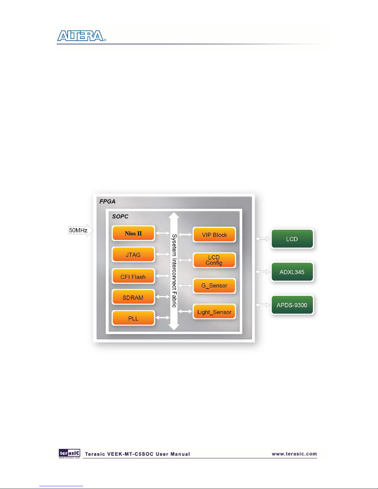
Figure 2-3 gives the block diagram of the VEEK-MT-C5SOC board. VEEK-MT-C5SOC is a
Cyclone V SoC development board and a Multi-touch LCD Camera Card (MTLC) combination
connected via the HSMC connector. MTLC module is not only equipped with a 7"LCD screen, it
also equips a 5-Megapixel digital image sensor module, G-sensor and Light sensor. All these
sensors connect to the FPGA device via the HSMC connector, so they can be controlled and directly
used by the FPGA device.
Figure 2-3 Block Diagram of VEEK-MT-C5SOC
Page 12

10
Chapter 3
Chapter 3Chapter 3
Chapter 3
Using
Using Using
Using VEEK
VEEKVEEK
VEEK----MT
MTMT
MT----C5SOC
C5SOCC5SOC
C5SOC
This section describes the detailed information of the components, connectors, and pin assignments
of the VEEK-MT-C5SOC.
33..1
1
UUssiinngg tthhee CCyycclloonnee®® VV SSXX SSooCC FFPPGGAA
The VEEK-MT-C5SOC is composed of Cyclone V SoC development board and 7" touch panel
daughter card. In this combination, the Cyclone V SoC development board which equips the FPGA
device is considered as the main part. Therefore, it can refer to the User Guide
(http://www.altera.com/literature/ug/ug_cv_soc_dev_kit.pdf) of Cyclone V SoC development board
on the FPGA device configuration and board setup.
33..2
2
UUssiinngg tthhee 77”” LLCCDD CCaappaacciittiivvee TToouucchh SSccrreeeenn
The VEEK-MT-C5SOC features a 7-inch capacitive amorphous TFT-LCD panel. The LCD touch
screen offers resolution of (800x480) to provide users the best display quality for developing
applications. The LCD panel supports 24-bit parallel RGB data interface.
The VEEK-MT-C5SOC is also equipped with a Touch controller, which can read the coordinates of
the touch points through the serial port interface of the Touch controller.
To display images on the LCD panel correctly, the RGB color data along with the data enable and
clock signals must act according to the timing specification of the LCD touch panel as shown in
Table 3-1. Table 3-2 gives the pin assignment information of the LCD touch panel.
Table 3-1 LCD timing specifications
ITEM SYMBOL
MIN.
TYP. MAX. UNIT NOTE
DCLK
Dot Clock 1/tCLK 33 MHZ
DCLK pulse duty Tcwh 40 50 60 %
DE
Setup time Tesu 8 ns
Hold time Tehd 8 ns
Horizontal period tH 1056 tCLK
Horizontal Valid tHA 800 tCLK
Page 13

11
Horizontal Blank tHB 256 tCLK
Vertical Period tV 525 tH
Vertical Valid tVA 480 tH
Vertical Blank tVB 45 tH
SYNC
HSYNC setup time Thst 8 ns
HSYNC hold time Thhd 8 ns
VSYNC Setup Time Tvst 8 ns
VSYNC Hold Time Tvhd 8 ns
Horizontal Period th 1056 tCLK
Horizontal Pulse Width
thpw 30 tCLK
thb+thpw=46DCLK
is fixed Horizontal Back Porch
thb 16 tCLK
Horizontal Front Porch thfp 210 tCLK
Horizontal Valid thd 800 tCLK
Vertical Period tv 525 th
Vertical Pulse Width tvpw 13 th tvpw + tvb =
23th
is fixed Vertical Back Porch tvb 10 th
Vertical Front Porch tvfp 22 th
Vertical Valid tvd 480 th
DATA
Setup time Tdsu 8 ns
Hold time Tdsu 8 ns
Table 3-2 Pin assignment of the LCD touch panel
Signal Name
FPGA Pin
No.
Description I/O Standard
LCD_B0
C4
LCD blue data bus bit 0 2.5V
LCD_B1
D5
LCD blue data bus bit 1 2.5V
LCD_B2
A3
LCD blue data bus bit 2 2.5V
LCD_B3
A4
LCD blue data bus bit 3 2.5V
LCD_B4
E11
LCD blue data bus bit 4 2.5V
LCD_B5
F11
LCD blue data bus bit 5 2.5V
LCD_B6
F8
LCD blue data bus bit 6 2.5V
LCD_B7
F9
LCD blue data bus bit 7 2.5V
LCD_DCLK
E6
LCD Clock 2.5V
LCD_DE
C3
Data Enable signal 2.5V
LCD_DIM
F13
LCD backlight enable 2.5V
LCD_DITH
H8
Dithering setting 2.5V
LCD_G0
D12
LCD green data bus bit 0 2.5V
LCD_G1
E12
LCD green data bus bit 1 2.5V
LCD_G2
D10
LCD green data bus bit 2 2.5V
Page 14
12
LCD_G3
D11
LCD green data bus bit 3 2.5V
LCD_G4
D9
LCD green data bus bit 4 2.5V
LCD_G5
E9
LCD green data bus bit 5 2.5V
LCD_G6
B5
LCD green data bus bit 6 2.5V
LCD_G7
B6
LCD green data bus bit 7 2.5V
LCD_HSD
C12
Horizontal sync input. 2.5V
LCD_MODE
G8
DE/SYNC mode select 2.5V
LCD_POWER_CTL
G10
LCD power control 2.5V
LCD_R0
A13
LCD red data bus bit 0 2.5V
LCD_R1
B13
LCD red data bus bit 1 2.5V
LCD_R2
C9
LCD red data bus bit 2 2.5V
LCD_R3
C10
LCD red data bus bit 3 2.5V
LCD_R4
B8
LCD red data bus bit 4 2.5V
LCD_R5
C8
LCD red data bus bit 5 2.5V
LCD_R6
A8
LCD red data bus bit 6 2.5V
LCD_R7
A9
LCD red data bus bit 7 2.5V
LCD_RSTB
B1
Global reset pin 2.5V
LCD_SHLR
B3
Left or Right Display Control 2.5V
LCD_UPDN
B2
Up / Down Display Control 2.5V
LCD_VSD
B11
Vertical sync input. 2.5V
TOUCH _I2C_SCL
F14
touch I2C clock 2.5V
TOUCH _I2C_SDA
F15
touch I2C data 2.5V
TOUCH _INT_n
B12
touch interrupt 2.5V
33..3
3
UUssiinngg 55--mmeeggaappiixxeell DDiiggiittaall IImmaaggee SSeennssoorr
The VEEK-MT-C5SOC is equipped with a 5-megapixel digital image sensor that provides an active
imaging array of 2,592H x 1,944V. It features low-noise CMOS imaging technology that achieves
CCD image quality. In addition, it incorporates sophisticated camera functions on-chip such as
windowing, column and row skip mode, and snapshot mode.
The sensor can be operated in its default mode or programmed by the user through a simple
two-wire serial interface for frame size, exposure, gain settings, and other parameters. Table 3-3
contains the pin names and descriptions of the image sensor module.
Page 15

13
Table 3-3 Pin assignment of the CMOS sensor
Signal Name
FPGA Pin
No.
Description I/O Standard
CAMERA_PIXCLK
AG2
Pixel clock 2.5V
CAMERA_D0
H14
Pixel data bit 0 2.5V
CAMERA_D1
G13
Pixel data bit 1 2.5V
CAMERA_D2
K12
Pixel data bit 2 2.5V
CAMERA_D3
J12
Pixel data bit 3 2.5V
CAMERA_D4
J10
Pixel data bit 4 2.5V
CAMERA_D5
J9
Pixel data bit 5 2.5V
CAMERA_D6
K7
Pixel data bit 6 2.5V
CAMERA_D7
K8
Pixel data bit 7 2.5V
CAMERA_D8
G12
Pixel data bit 8 2.5V
CAMERA_D9
G11
Pixel data bit 9 2.5V
CAMERA_D10
J7
Pixel data bit 10 2.5V
CAMERA_D11
H7
Pixel data bit 11 2.5V
CAMERA_STROBE
D6
Snapshot strobe 2.5V
CAMERA_LVAL
D7
Line valid 2.5V
CAMERA_FVAL
E8
Frame valid 2.5V
CAMERA_RESET_n
E4
Image sensor reset 2.5V
CAMERA_SCLK
AF9
Serial clock 2.5V
CAMERA_TRIGGER
C5
Snapshot trigger 2.5V
CAMERA_SDATA
AG7
Serial data 2.5V
CAMERA_XCLKIN
AJ2
External input clock 2.5V
33..4
4
UUssiinngg tthhee DDiiggiittaall AAcccceelleerroommeetteerr
The VEEK-MT-C5SOC is equipped with a digital accelerometer sensor module. The ADXL345 is a
small, thin, and ultralow-power-consumption 3-axis accelerometer with high resolution
measurement. Digitalized output is formatted as 16-bit twos complement and could be accessed
either using SPI interface or I2C interface. This chip uses the 3.3V CMOS signaling standard. Main
applications include medical instrumentation, industrial instrumentation, personal electronic aid and
hard disk drive protection etc. Some of the key features of this device are listed below. For more
detailed information of better using this chip, please refer to its datasheet which is available on
manufacturer’s website or under the /datasheet folder of the system CD.
Page 16

14
Table 3-4 contains the pin names and descriptions of the G sensor module.
Signal Name FPGA Pin No. Description I/O Standard
GSENSOR_INT1 E3 Interrupt 1 output 2.5V
GSENSOR_INT2 E2 Interrupt 2 output 2.5V
GSENSOR_CS_n D4 Chip Select 2.5V
GSENSOR_ALT_ADDR E1 I2C Address Select 2.5V
GSENSOR_SDA_SDI_SDIO D1 Serial Data 2.5V
GSENSOR_SCL_SCLK D2 Serial Communications Clock 2.5V
33..5
5
UUssiinngg tthhee AAmmbbiieenntt LLiigghhtt SSeennssoorr
The APDS-9300 is a low-voltage digital ambient light sensor that converts light intensity to digital
signal output capable of direct I2C communication. Each device consists of one broadband
photodiode (visible plus infrared) and one infrared photodiode. Two integrating ADCs convert the
photodiode currents to a digital output that represents the irradiance measured on each channel. This
digital output can be input to a microprocessor where luminance (ambient light level) in lux is
derived using an empirical formula to approximate the human-eye response. For more detailed
information of better using this chip, please refer to its datasheet which is available on
manufacturer’s website or under the /datasheet folder of the system CD.
Table 3-5 contains the pin names and descriptions of the ambient light sensor module.
Signal Name FPGA Pin No. Description I/O Standard
LSENSOR_ADDR_SEL A6 Chip select 2.5V
LSENSOR_INT B7 Interrupt output 2.5V
LSENSOR_SCL A5 Serial Communications Clock 2.5V
LSENSOR_SDA C7 Serial Data 2.5V
33..6
6
UUssiinngg TTeerraassiicc MMuullttii--ttoouucchh IIPP
Terasic Multi-touch IP is provided for developers to retrieve user inputs, including multi-touch
gestures and single-touch. The file name of this IP is i2c_touch_config and it is encrypted. To
compile projects with the IP, users need to install the IP license first. For license installation, please
refer to section 1.2 Setup License for Terasic Multi-touch IP in this document. The license file
is located at:
VEEK-MT-C5SOC System CD\License\license_multi_touch.dat
The IP decodes I2C information and outputs coordinate and gesture information. The IP interface is
shown below:
Page 17

15
The signal purpose of the IP is described in Table 3-6. The IP requires a 50 MHz signal as a
reference clock to the iCLK pin and system reset signal to iRSTN. iTRIG, I2C_SCLK, and
IC2_SDAT pins should be connected of the TOUCH_INT_n, TOUCH_I2C_SCL, and
TOUCH_I2C_SDA signals in the 2x20 GPIO header respectively. When oREADY rises, it means
there is touch activity, and associated information is given in the oREG_X1, oREG_Y1, oREG_X2,
oREG_Y2, oREG_TOUCH_COUNT, and oREG_GESTURE pins.
For the control application, when touch activity occurs, it should check whether the value of
oREG_GESTURE matched a pre-defined gesture ID defined in Table 3-7. If it is not a gesture, it
means a single-touch has occurred and the relative X/Y coordinates can be derived from oREG_X1
and oREG_Y1.
Table 3-6 Interface Definitions of Terasic Multi-touch IP
Pin Name Direction Description
iCLK Input Connect to 50MHz Clock
iRSTN Input Connect to system reset signal
iTRIG Input Connect to Interrupt Pin of Touch IC
oREADY Output Rising Trigger when following six output data
is valid
oREG_X1 Output 10-bits X coordinate of first touch point
oREG_Y1 Output 9-bits Y coordinate of first touch point
oREG_X2 Output 10-bits X coordinate of second touch point
oREG_Y2 Output 9-bits Y coordinate of second touch point
oREG_TOUCH_COUNT Output 2-bits touch count. Valid value is 0, 1, or 2.
oREG_GESTURE Output 8-bits gesture ID (See
Table 3-7)
I2C_SCLK Output Connect to I2C Clock Pin of Touch IC
I2C_SDAT Inout Connect to I2C Data Pin of Touch IC
The supported gestures and IDs are shown in Table 3-7.
Page 18

16
Table 3-7 Gestures
Gesture ID (hex)
One Point Gesture
North 0x10
North-East 0x12
East 0x14
South-East 0x16
South 0x18
South-West 0x1A
West 0x1C
North-West 0x1E
Rotate Clockwise 0x28
Rotate Anti-clockwise 0x29
Click 0x20
Double Click 0x22
Two Point Gesture
North 0x30
North-East 0x32
East 0x34
South-East 0x36
South 0x38
South-West 0x3A
West 0x3C
North-West 0x3E
Click 0x40
Zoom In 0x48
Zoom Out 0x49
Note: The Terasic IP Multi-touch IP can also be found under the \IP folder in the system CD as
well as the \IP folder in the reference designs.
Page 19

17
Chapter 4
Chapter 4Chapter 4
Chapter 4
VEEK
VEEKVEEK
VEEK----MT
MTMT
MT----C5SOC
C5SOCC5SOC
C5SOC Demonstrations
DemonstrationsDemonstrations
Demonstrations
This chapter gives detailed description of the provided bundles of exclusive demonstrations
implemented on VEEK-MT-C5SOC. These demonstrations are particularly designed (or ported) for
VEEK-MT-C5SOC, with the goal of showing the potential capabilities of the kit and showcase the
unique benefits of FPGA-based SOPC systems such as reducing BOM costs by integrating
powerful graphics and video processing circuits within the FPGA.
44..1
1
SSyysstteemm RReeqquuiirreemmeennttss
To run and recompile the demonstrations, you should:
•••• Install Altera Quartus II 13.0 and NIOS II EDS 13.0 or a later edition on the host computer
•••• Install the USB-Blaster II driver software.
•••• Copy the entire demonstrations folder from the VEEK-MT-C5SOC system CD to your host
computer
44..2
2
PPaaiinntteerr DDeemmoonnssttrraattiioonn
This chapter shows how to control LCD and touch controller to establish a paint demo based on
Qsys and Altera VIP Suite. The demonstration shows how multi-touch gestures and single-touch
coordinates operate.
Figure 4-1 shows the hardware system block diagram of this demonstration. For LCD display
processing, the reference design is developed based on the Altera Video and Image Processing Suite
(VIP). The Frame Reader VIP is used for reading display content from the associated video memory,
and VIP Video Out is used to display the display content. The display content is filled by NIOS II
processor according to users’ input.
For multi-touch processing, a Terasic Memory-Mapped IP is used to retrieve the user input,
including multi-touch gesture and single-touch resolution. Note, the IP is encrypted, so the license
should be installed before compiling the Quartus II project. For IP--usage details please refer to the
section 3.6 Using Terasic Multi-touch IP in this document.
Page 20

18
Figure 4-1 Block diagram of the Painter demonstration
Demonstration Source Code
•••• Project directory: Painter
•••• Bit stream used: Painter.sof
•••• Nios II Workspace: Painter \Software
Demonstration Batch File
Demo Batch File Folder: Painter \demo_batch
The demo batch file includes the following files:
•••• Batch File: test.bat, test_bashrc
•••• FPGA Configure File: Painter.sof
•••• Nios II Program: Painter.elf
Demonstration Setup
•••• Make sure Quartus II and Nios II are installed on your PC
•••• Power on the Cyclone V SoC development board
•••• Connect USB-Blaster to the Cyclone V SoC development board and install USB-Blaster driver
if necessary
Page 21

19
•••• Execute the demo batch file “test.bat” under the batch file folder, Painter \demo_batch
• After Nios II program is downloaded and executed successfully, you will see a painter GUI in
the LCD. Figure 4-2 shows the GUI of the Painter Demo.
•••• The GUI is classified into three areas: Palette, Canvas, and Gesture. Users can select pen color
from the color palette and start painting in the Canvas area. If gesture is detected, the associated
gesture symbol is shown in the gesture area. To clear canvas content, click the “Clear” button.
•••• Figure 4-3 shows the photo when users paint in the canvas area. Figure 4-4 shows the phone
when counter-clockwise rotation gesture is detected. Figure 4-5 shows the photo when zoom-in
gesture is detected.
Figure 4-2 GUI of Painter Demo
Page 22

20
Figure 4-3 Single Touch Painting
Figure 4-4 Counter-clockwise Rotation Gesture
Page 23
21
Figure 4-5 Zoom-in Gesture
Note: execute the test.bat under Picture_Viewer\demo_batch will automatically download
the .sof and .elf file.
44..3
3
CCaammeerraa AApppplliiccaattiioonn
This demonstration shows a digital camera reference design using the 5-Megapixel CMOS sensor
and 8-inch LCD modules on the VEEK-MT-C5SOC. The CMOS sensor module sends the raw
image data to FPGA on the Altera Cyclone® V SoC board, the FPGA on the board handles image
processing part and converts the data to RGB format to display on the LCD module. The I2C
Sensor Configuration module is used to configure the CMOS sensor module. Figure 4-6 shows the
block diagram of the demonstration.
As soon as the configuration code is downloaded into the FPGA, the I2C Sensor Configuration
block will initial the CMOS sensor via I2C interface. The CMOS sensor is configured as follow:
•••• Row and Column Size: 800 * 480
•••• Exposure time: Adjustable
•••• Pix clock: MCLK*2 = 25*2 = 50MHz
•••• Readout modes: Binning
•••• Mirror mode: Line mirrored
According to the settings, we can calculate the CMOS sensor output frame rate is about 44.4 fps.
Page 24

22
After the configuration, The CMOS sensor starts to capture and output image data streams, the
CMOS sensor Capture block extracts the valid pix data streams based on the synchronous signals
from the CMOS sensor. The data streams are generated in Bayer Color Pattern format. So it’s then
converted to RGB data streams by the RAW2RGB block.
After that, the Multi-Port SDRAM Controller acquires and writes the RGB data streams to the
SDRAM which performs as a frame buffer. The Multi-Port SDRAM Controller has two write ports
and read ports also with 16-bit data width each. The writing clock is the same as CMOS sensor pix
clock, and the reading clock is provided by the LCD Controller, which is 33MHz.
Finally, the LCD controller fetches the RGB data from the buffer and displays it on the LCD panel
continuously. Because the resolution and timing of the LCD is compatible with WVGA@800*480,
the LCD controller generates the same timing and the frame rate can achieve about 25 fps.
For the objective of a better visual effect, the CMOS sensor is configured to enable the left right
mirror mode. User could disable this functionality by modifying the related register value being
written to CMOS controller chip.
Figure 4-6 Block diagram of the digital camera design
Demonstration Source Code
•••• Project directory: Camera
•••• Bit stream used: Camera.sof
Page 25

23
Demonstration Batch File
Demo Batch File Folder: Camera\demo_batch
The demo batch file includes the following files:
•••• Batch File: test.bat
•••• FPGA Configure File: Camera.sof
Demonstration Setup
•••• Load the bit stream into FPGA by executing the batch file ‘test.bat’ under Camera\demo_batch\
folder
•••• The system enters the FREE RUN mode automatically. Press S6 on the Altera Cyclone® V SoC
board to reset the circuit
•••• User can use the SW1.5 and S5 to set the exposure time for brightness adjustment of the image
captured. When SW1.5 is set to Off, the brightness of image will be increased as S5 is pressed
longer. If SW1.5 is set to On, the brightness of image will be decreased as S5 is pressed shorter
•••• User can use SW1.8 to mirror image of the line. However, remember to press S6 after toggle
SW1.8]
Note: execute the test.bat under Camera\demo_batch will automatically download
the .sof file.
Table 4-1 and Figure 4-7 summarizes the functional keys of the digital camera. Figure 4-8 gives a
run-time photograph of the demonstration.
Table 4-1 The functional keys of the digital camera demonstration
Component Function Description
S6 Reset circuit
S5 Set the new exposure time (use with SW1.5
)
SW1.5
Off: Extend the exposure time
On: Shorten the exposure time
S1.8
Mirror image (use with S6)
Page 26

24
Figure 4-7 Block diagram of the digital camera design
Figure 4-8 Screen shot of the VEEK-MT-C5SOC camera demonstration
Page 27
25
44..4
4
DDiiggiittaall AAcccceelleerroommeetteerr DDeemmoonnssttrraattiioonn
This demonstration shows a bubble level implementation based on a digital accelerometer. We use
I2C protocol to control the ADXL345 digital accelerometer, and the APDS-9300 Miniature Ambient
Light Photo Sensor. The LCD displays the interface of our game. When tilting the
VEEK-MT-C5SOC, the ADXL345 measures the static acceleration of gravity. In our Nios II
software, we compute the change of angle in the x-axis and y-axis, and show angle data in the LCD
display. The value of light sensor will change as the brightness changes around the light-sensor.
Figure 4-9 shows the hardware system block diagram of this demonstration. The system is clocked
by an external 50MHz Oscillator. Through the internal PLL module, the generated 150MHz clock is
used for Nios II processor and other components, and there is also 10MHz for low-speed
peripherals.
Figure 4-9 Block diagram of the digital accelerometer demonstration
Demonstration Source Code
•••• Project directory: G_sensor
•••• Bit stream used: G_sensor.sof
•••• Nios II Workspace: G_sensor\Software
Page 28

26
Demonstration Batch File
Demo Batch File Folder: G_sensor\demo_batch
The demo batch includes the following files:
•••• Batch File: G_sensor.bat, test_bashrc
•••• FPGA Configure File: G_sensor.sof
•••• Nios II Program: G_sensor.elf
Demonstration Setup
•••• Load the bit stream into the FPGA on the VEEK-MT-C5SOC.
•••• Run the Nios II Software under the workspace G_sensor\Software (Note*).
•••• After the Nios II program is downloaded and executed successfully, a prompt message will be
displayed in nios2-terminal: “its ADXL345’s ID = e5”.
•••• Tilt the VEEK-MT-C5SOC to all directions, and you will find that the angle of the g-sensor and
value of light sensor will change. When turning the board from -80º to -10º and from 10º to 80
º in Y-axis, or from 10ºto 80º and from -80º to -10º in Y-axis, the image will invert Figure
4-10 shows the demonstration in action.
Figure 4-10 Digital Accelerometer demonstration
Page 29

27
Note:
Execute G_sensor \demo_batch\test.bat to download .sof and .elf files.
Page 30

28
Chapter 5
Chapter 5Chapter 5
Chapter 5
Appendix
AppendixAppendix
Appendix
55..1
1
RReevviissiioonn HHiissttoorryy
Version Change Log
V1.0 Initial Version (Preliminary)
55..2
2
CCooppyyrriigghhtt SSttaatteemmeenntt
Copyright © 2013 Terasic Technologies. All rights reserved.
 Loading...