

Page 1
Page 2

TSoM User Manual
1 www.terasic.com
March 8, 2019
TABLE OF CONTENTS
Chapter 1 Introduction ................................................................................................................... 2
1.1 TSoM Design Package ........................................................................................................................ 2
1.2 Getting Help ........................................................................................................................................ 2
Chapter 2 Board Specification ......................................................................................................... 3
2.1 Layout and Components ..................................................................................................................... 3
2.2 Block Diagram .................................................................................................................................... 3
2.3 Mechanical Specifications .................................................................................................................. 5
2.4 Power Requirement ............................................................................................................................. 5
Chapter 3 System Interface ............................................................................................................. 7
3.1 Device Configuration .......................................................................................................................... 7
3.2 Clock System .................................................................................................................................... 10
3.3 Reset System ..................................................................................................................................... 11
3.4 260-pin Edge Connector ................................................................................................................... 11
Chapter 4 HPS Fabric Components ............................................................................................... 13
4.1 USB 2.0 ............................................................................................................................................. 13
4.2 Gigabit Ethernet ................................................................................................................................ 14
4.3 eMMC ............................................................................................................................................... 15
4.4 HPS 3.3V GPIO ................................................................................................................................ 16
4.5 DDR3 ................................................................................................................................................ 18
Chapter 5 FPGA Fabric Components ............................................................................................. 21
5.1 DDR3 ................................................................................................................................................ 21
5.2 FPGA IOs on 260-Pin Edge Connector ............................................................................................ 23
Page 3

TSoM User Manual
2 www.terasic.com
March 8, 2019
Chapter 1
Introduction
TSoM (Terasic SoC System on Module) are small, integrated single-board computers with
Cyclone® V SoCs at the core. The SoC SoM includes DDR3 memory, flash memory, power
management, common interface controllers, and board support package (BSP) software to help you
create a fully customized embedded design without starting from scratch.
11..1
1
TTSSooMM DDeessiiggnn PPaacckkaaggee
The TSoM design package contains all the documents and supporting materials associated with
TSoM module, including the user manual, system builder, reference designs, and device datasheets.
Users can download this design package from the link: http://TSoM.terasic.com/cd.
11..2
2
GGeettttiinngg HHeellpp
Here are the addresses where you can get help if you encounter any problems:
Terasic Technologies
9F., No.176, Sec.2, Gongdao 5th Rd, East Dist, Hsinchu City, 30070. Taiwan
Email: support@terasic.com
Tel.: +886-3-575-0880
Website: TSoM.terasic.com
Page 4
TSoM User Manual
3 www.terasic.com
March 8, 2019
Chapter 2
Board Specification
This chapter provides an introduction to the features and design characteristics of the module.
22..1
1
LLaayyoouutt aanndd CCoommppoonneennttss
Figure 2-1 shows a photograph of the module. It depicts the layout of the module and indicates the
location of the connectors and key components.
Note: The Cyclone® V system-on-a-chip (SoC) is composed of two distinct portions: a single or
dual-core Arm® Cortex® A9 hard processor system (HPS) and an FPGA. The HPS architecture
integrates a wide set of peripherals that reduce board size and increase performance within a
system.
Figure 2-1 Mechanical Layout of the TSoM Module
22..2
2
BBlloocckk DDiiaaggrraamm
Figure 2-2 is the block diagram of the module. The most FPGA I/Os of TSoM module are all
connected to the onboard 260-pin Edge connector, then it’s easy to connected to customer’s main
board.
Page 5
TSoM User Manual
4 www.terasic.com
March 8, 2019
Figure 2-2 Block diagram of the TSoM Module
Detailed information about Figure 2-2 are listed below.
◼ Module:
⚫ FPGA: Cyclone V SE 5CSEBA6U23I7NDK (110K LEs)
⚫ Interface: DDR4 Edge (include 3.3V power source)
⚫ Dimension: 50 mm x 70 mm
◼ FPGA Fabric side:
⚫ DDR3 SDRAM 1GB, 32bit – 303MHz (Soft IP)
⚫ LVDS Transmitter x15 & LVDS Receiver x17 pairs & GPIO x3 ( Total GPIO x67)
⚫ Optional EPCS64
◼ HPS Fabric side:
⚫ Boot Selection DIP Switch: boot from eMMC or MicroSD Card
⚫ DDR3 SDRAM 1GB, 32bit - 400MHz
⚫ USB 2.0 PHY
⚫ Gigabit Ethernet PHY
⚫ 3.3V GPIO x25 (Can/UART/SPI/I2C/Trace Buses)
⚫ 1.5V GPI x4 (Input pins)
⚫ Optional eMMC 8GB
Page 6
TSoM User Manual
5 www.terasic.com
March 8, 2019
22..3
3
MMeecchhaanniiccaall SSppeecciiffiiccaattiioonnss
Figure 2-3 is the Mechanical Layout of TSoM module and Table 2-1 shows the mechanical data of
the TSoM module.
Figure 2-3 Mechanical Layout of the TSoM Module
Table 2-1 Mechanical data of the TSoM Module
Symbol
Value
Size
70 x50mm
22..4
4
PPoowweerr RReeqquuiirreemmeenntt
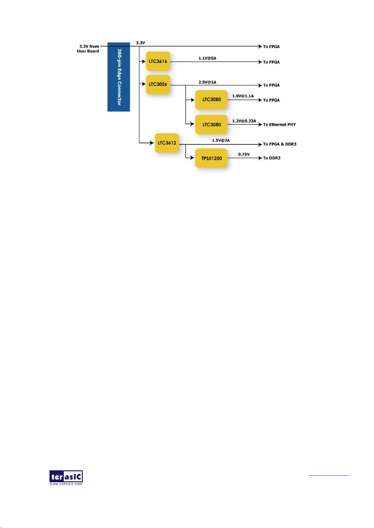
The TSoM module is powered by the 260-pin edge connector. The user only needs to supply
3.3V/6A to the 260-pin edge connector of the TSoM module. The power circuit on the TSoM
module can convert 3.3V to 1.1V/1.2V/1.5V/1.8V/2.5V, which then is supplied to the FPGA and
other components. Figure 2-4 shows the power tree of TSoM module.
Page 7
TSoM User Manual
6 www.terasic.com
March 8, 2019
Figure 2-4 Power Tree of the TSoM Module
Page 8
TSoM User Manual
7 www.terasic.com
March 8, 2019
Chapter 3
System Interface
This chapter will introduce the system level interfaces on the TSoM module. Users can get the Boot
method of the HPS, the clock and reset system on the module, and the detailed pin distribution of
the 260-pin edge connector connected externally.
33..1
1
DDeevviiccee CCoonnffiigguurraattiioonn
This section describes the various interfaces on the TSoM module that can be configured with
FPGAs and HPS. Users can learn about the JTAG interface on TSoM module, the sources that can
be used as boot devices on the HPS side, and the configuration chips on the FPGA side through this
section.
◼ JTAG
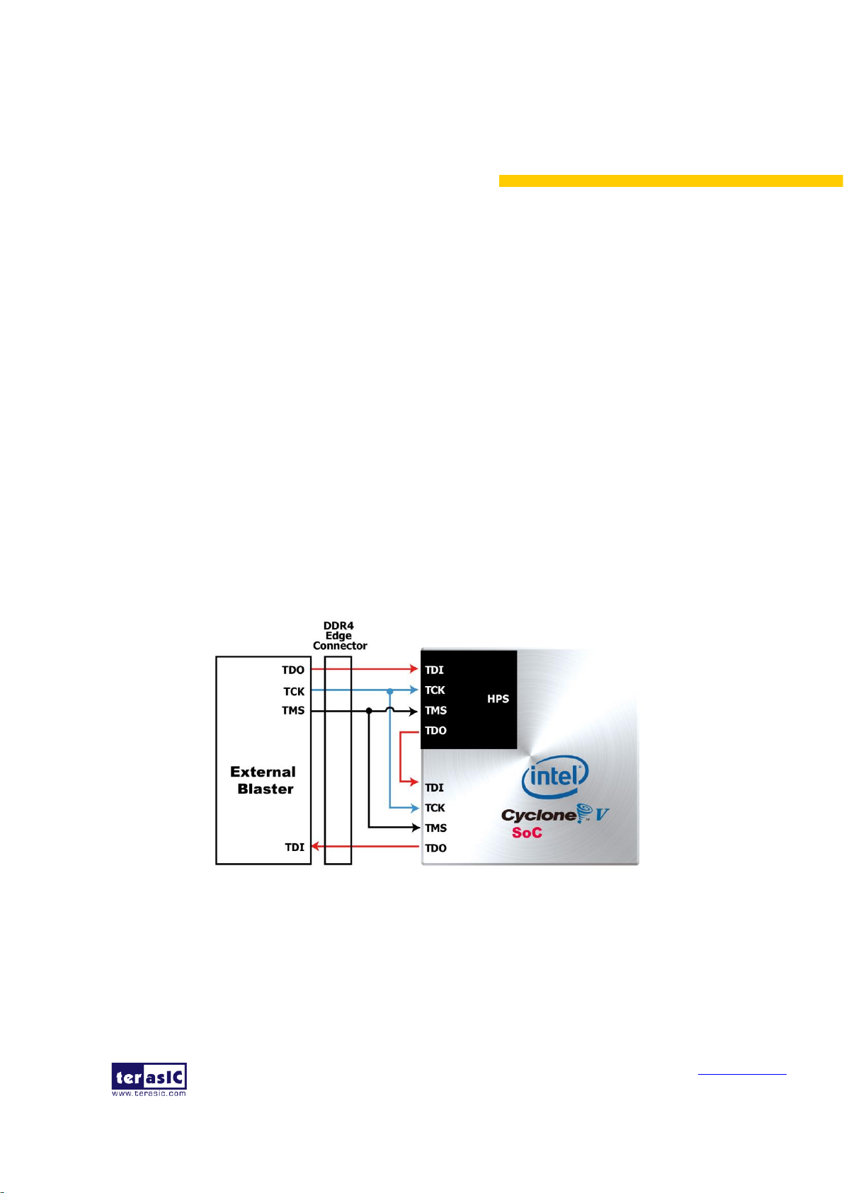
Figure 3-1 is the JTAG interface on TSoM module, users can configure the FPGA from host PC
through the JTAG interface, the HPS is also included in the JTAG chain on TSoM module which
allows user to debug and develop the HPS ARM through the JTAG interface. The JTAG signals
come from the 260-pin edge connector, USB Blaster circuit or external Blaster connector need to be
reserved on customer’s main board for the JTAG communication with the FPGA on the TSoM
module.
Figure 3-1 JTAG Interface on the TSoM Module
◼ HPS Boot Mode
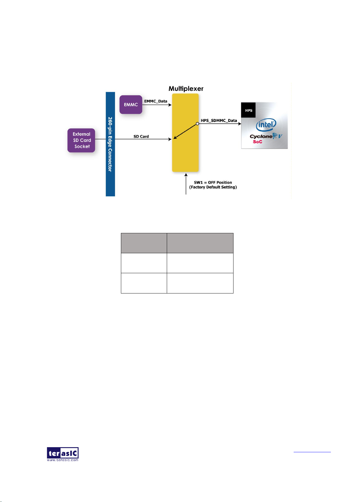
As shown in Figure 3-2, The TSoM module has two HPS boot source, one is the 8G eMMC
(Embedded Multimedia Card) memory, another is the external boot device on the 260-pin edge
connector. When the 260-pin edge connector is connected to the main board which contains
Page 9
TSoM User Manual
8 www.terasic.com
March 8, 2019
external SD card socket or QSPI flash, the external SD card socket is used as the HPS boot source.
Only one of the two boot sources can be chosen for the boot source on TSoM board . User can
control the multiplexer and choose eMMC or external boot device as the boot source through SW1,
as shown in Table 3-1.
Figure 3-2 Boot Source on the TSoM Module
Table 3-1 SW1 Setting for Boot Source
SW1 Status
Boot Source
ON Position
eMMC device
OFF Position
External SD card
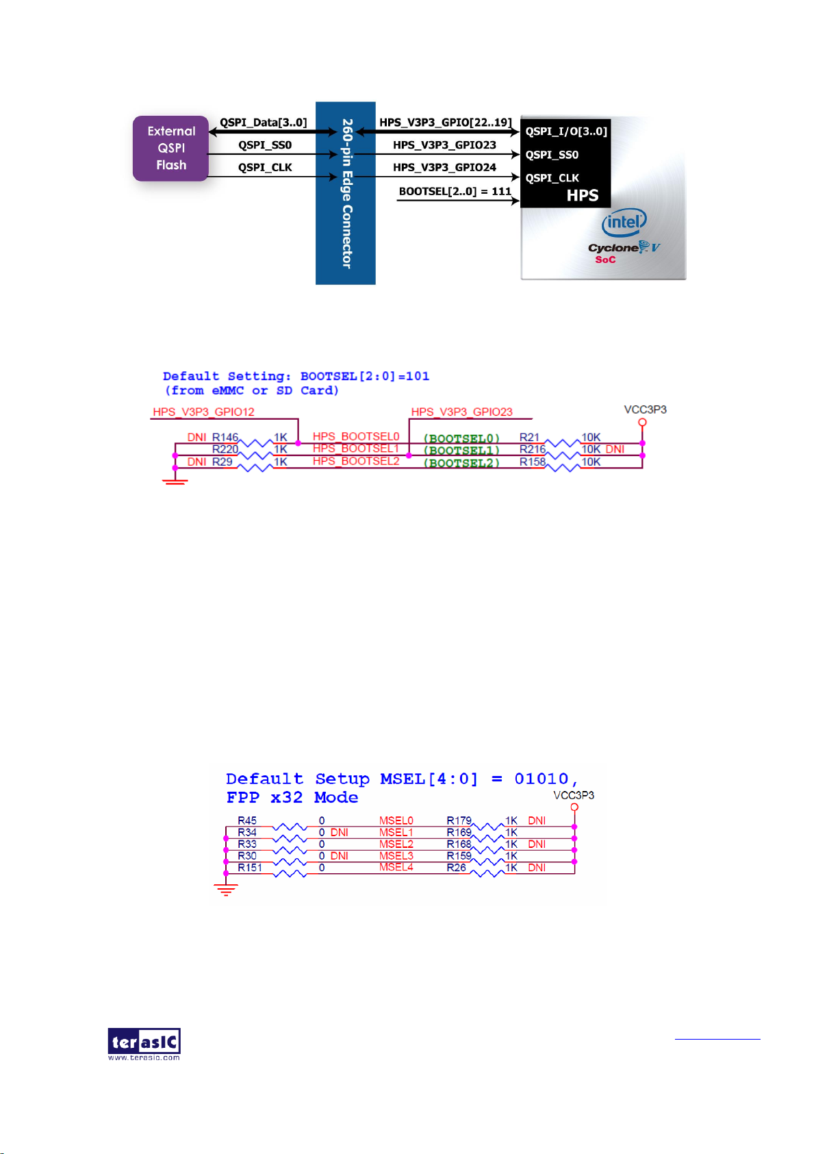
In addition, the QSPI interface on the TSoM HPS side is connected to the 260-pin edge connector
(HPS_V3P3_GPIO[24..19]), so user also can use the external QSPI flash as the HSP boot source by
connecting QSPI flash on the external main board to the TSoM 260-pin edge connector. But please
note that the HPS boot source setting control pins (HPS_BOOTSEL[2:0]) are by default set as
SD/MMC mode by the resistors, as shown in Figure 3-3. To set the external QSPI flash as the HPS
source, user needs to set HPS_BOOTSEL[2:0] as "111". Figure 3-4 shows the resistors setting.
Page 10
TSoM User Manual
9 www.terasic.com
March 8, 2019
Figure 3-3 Using QSPI Flash as HPS boot source on the TSoM Module
Figure 3-4 HPS_BOTSEL[2..0] resistors setting
◼ EPCS
There is an EPCS64 configuration device reserved on the TSoM module. The EPCS device is a
flash memory device that can store configuration data that you use for FPGA configuration purpose
after powering on. You can use the EPCS device on all FPGAs that support AS x1configuration
scheme. User needs to modify the setting resistors of the FPGA MSEL pins if they want to use the
EPCS64 device. The factory setting of the MSEL[4:0] on the TSoM module is FPPx32 mode which
is used to configure FPGA from HPS. If user wants to the EPCS64 device, he can modify the
resistors as shown in Figure 3-5 to set the MSEL[4:0] as "10010" to switch to AS mode. Figure 3-6
and Figure 3-7 show the resistors actual position on the TSoM module (Top and Bottom Side).
Figure 3-5 MSEL[4:0] Setting Resistors (FPPx32 Mode)
Page 11
TSoM User Manual
10
www.terasic.com
March 8, 2019
Figure 3-6 MSEL[4:0] Setting Resistors on the TSoM Module (Top Side)
Figure 3-7 MSEL[4:0] Setting Resistors on the TSoM Module (Bottom Side)
33..2
2
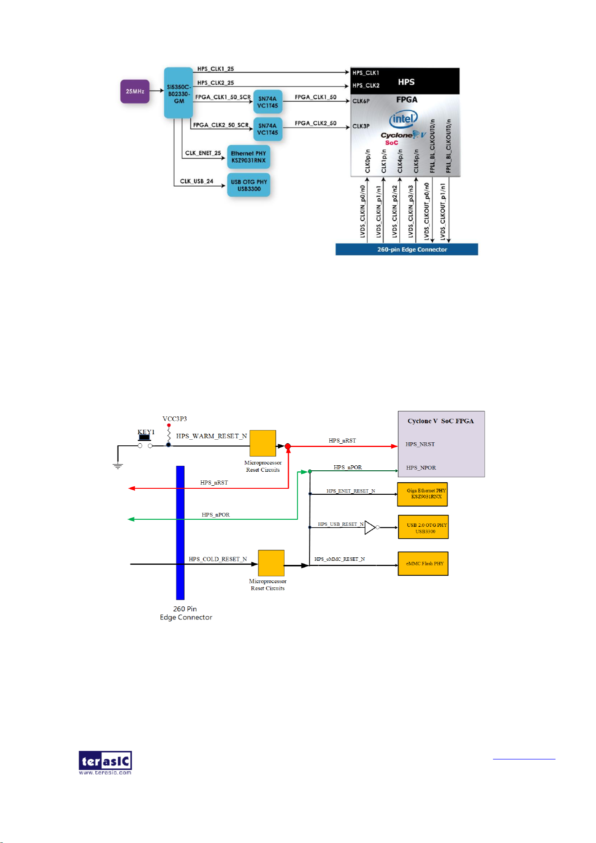
CClloocckk SSyysstteemm
The clock source on the TSoM module is provided by an Si5350C clock generator, which can
generate several groups of clocks for the devices on the TSoM module. The Si5350C generates
25MHz clock for the clock groups in the HPS, and provides two 50MHz clocks for the FPGA fabric
to drive customer’s design. Users also can multiple or devise the 50MHz clock through the FPGA
internal PLL. The Si5350C also provides clock for Ethernet PHY and USB OTG PHY.
Besides the Si5350C clock generator, users can input/output clock to the FPGA through the 260-pin
edge connector. There are four pairs LVDS clock inputs and two pairs LVDS clock outputs defined
on the 260-pin edge connector. These I/O are all connected to the dedicated clock pin of the FPGA
and can also be used as Single-end.
Page 12
TSoM User Manual
11
www.terasic.com
March 8, 2019
Figure 3-8 Clock System of the TSoM Module
33..3
3
RReesseett SSyysstteemm
The TSoM module provides warm reset and cold reset function for the HPS, as shown in the Figure
3-9. The cold reset comes from external mainboard and is used for HPS Ethernet PHY, USB OTG
PHY and eMMC memory through the 260-pin edge connector. The HPS_nRST pin is connected to
the 260-pin edge connector to be reserved for Intel DS-5 software tool to reset the HPS and connect
to the USB Blaster connector of the mainboard.
Figure 3-9 Reset System of the TSoM Module
33..4
4
226600--ppiinn EEddggee CCoonnnneeccttoorr
The TSoM module can be connected to external mainboard through the 260-pin edge connector
with the same specification (See Figure 3-10.), all the externally connected signals on the TSoM
module are communicated with and transferred to external main board through the edge connector,
which includes the FPGA and HPS I/O, the circuit of Ethernet PHY and USB OTG PHY, and also
Page 13

TSoM User Manual
12
www.terasic.com
March 8, 2019
provides system power and JTAG function. Users can refer to TSoM schematic for the detailed
signal connections. Users can connect the TSoM module to the main board that contains DDR4
SODIMM socket. Table 3-2 lists the several recommended DDR4 SODIMM sockets for reference.
Table A-1 in the Appendix chapter shows the detailed pin assignments of the 260-pin edge
connector.
Figure 3-10 260-pin edge connector on the TSoM module
Table 3-2 DDR4 SODIMM Socket
Vendor
Part
Number
Descriptions
TE
Connectivity
2309409-3
TE Connectivity DDR4 SODIMM 260P 5.2H STD
BellWether
80888-2023
DDR4 5.2H Connector 0.5mm Pitch, 260 Circuits Standard Type, SMT
Type, 10u"
Page 14
TSoM User Manual
13
www.terasic.com
March 8, 2019
Chapter 4
HPS Fabric
Components
The HPS and FPGA portions of the device each have their own pins. Pins are not freely shared
between the HPS and the FPGA fabric. This chapter will describe the peripherals connected to HPS
fabric, such as DDR3, Ethernet, eMMC and USB OTG.
44..1
1
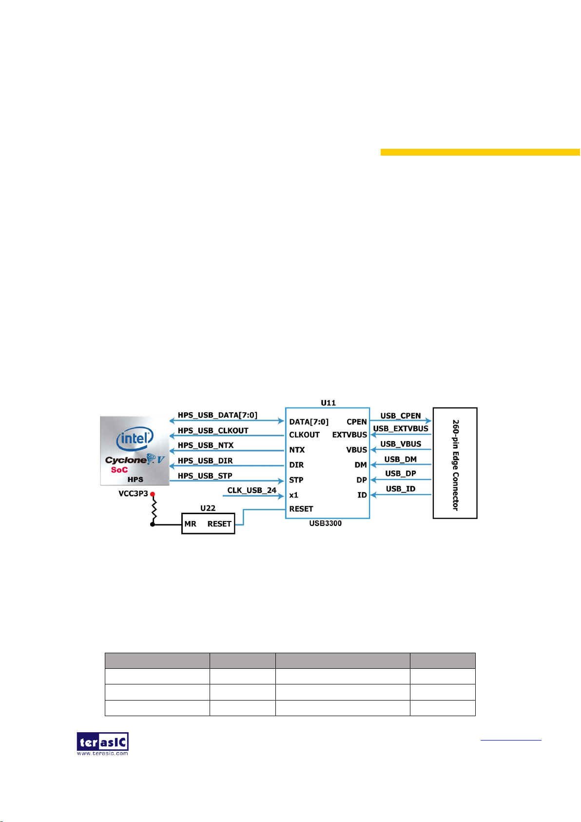
UUSSBB 22..00
The TSoM module has a single Host/Device (USB OTG) USB 2.0 PHY that connects to the SoC
device, the PHY can operate in USB host, USB device and USB On-The-Go (host and device
capable) modes. The PHY is connected to the 260-pin DDR4 SO-DIMM edge connector. The
following Figure 4-1 shows the connections between the USB 2.0 PHY and the HPS.
Note: There is only a USB 2.0 OTG PHY on the TSoM module (without any USB physical
interface), for using this function, users need to connect a TSoM Based Board (or other customized
expansion board) to implement the connection between the USB 2.0 OTG PHY and a USB physical
interface.
Figure 4-1 The Connections between the USB 2.0 PHY and the HPS
The ULPI interface is connected to HPS pins for use with the integrated USB controller. The USB
reset has a pull-down resistor and needs to be driven high to release the PHY from reset.
Table 4-1 lists the pin assignment of the USB 2.0 PHY and the HPS.
Table 4-1 the USB 2.0 PHY Pin Assignments
Signal Name
HPS Pin No.
Description
I/O Standard
HPS_USB_CLKOUT
PIN_G4
Reference Clock Output
3.3V
HPS_USB_DATA[1]
PIN_C10
HPS_USB_DATA[1]
3.3V
HPS_USB_DATA[1]
PIN_F5
HPS_USB_DATA[1]
3.3V
Page 15

TSoM User Manual
14
www.terasic.com
March 8, 2019
HPS_USB_DATA[2]
PIN_C9
HPS_USB_DATA[2]
3.3V
HPS_USB_DATA[3]
PIN_C4
HPS_USB_DATA[3]
3.3V
HPS_USB_DATA[4]
PIN_C8
HPS_USB_DATA[4]
3.3V
HPS_USB_DATA[5]
PIN_D4
HPS_USB_DATA[5]
3.3V
HPS_USB_DATA[6]
PIN_C7
HPS_USB_DATA[6]
3.3V
HPS_USB_DATA[7]
PIN_F4
HPS_USB_DATA[7]
3.3V
HPS_USB_DIR
PIN_E5
Direction of the Data Bus
3.3V
HPS_USB_NXT
PIN_D5
Throttle the Data
3.3V
HPS_USB_STP
PIN_C5
Stop Data Stream on the Bus
3.3V
44..2
2
GGiiggaabbiitt EEtthheerrnneett
The TSoM module supports a Giga Ethernet PHY. The Giga Ethernet uses the HPS RGMII
interface. The following Figure 4-2 describes the connections between Giga Ethernet PHY and the
HPS.
Note: There is only a Giga Ethernet PHY on the TSoM module (without any ethernet physical
interface, eg. J45), for using this function, users need to connect a TSoM Based Board (or other
customized expansion board) to implement the connection between the Giga Ethernet PHY and a
ethernet physical interface.
Figure 4-2 The connections between the Giga Ethernet interface and the HPS
The 1G Ethernet PHY is Micrel's KSZ9031. It uses an RGMII interface running at 125 MHz. The
125 MHz clock is generated by the KSZ9031 Giga Ethernet PHY.
The 1G Ethernet PHY analog signals (TX+/-, RX+/-) are connected to the 260-pin Edge Connector.
Two led signals from the GE PHY are also connected to the 260-pin Edge Connector. The Ethernet
MDC/MDIO signals are connected to the internal PHY and are not available on the 260-pin Edge
Connector.
Table 4-2 lists the pin assignment of Ethernet PHY and HPS.
Page 16

TSoM User Manual
15
www.terasic.com
March 8, 2019
Table 4-2 The Giga Ethernet interface Pin Assignments
Signal Name
FPGA Pin No.
Description
I/O Standard
HPS_ENET_TX_EN
PIN_A12
GMII and MII transmit enable
3.3V
HPS_ENET_TX_DATA[0]
PIN_A16
MII transmit data[0]
3.3V
HPS_ENET_TX_DATA[1]
PIN_J14
MII transmit data[1]
3.3V
HPS_ENET_TX_DATA[2]
PIN_A15
MII transmit data[2]
3.3V
HPS_ENET_TX_DATA[3]
PIN_D17
MII transmit data[3]
3.3V
HPS_ENET_RX_DV
PIN_J13
GMII and MII receive data valid
3.3V
HPS_ENET_RX_DATA[0]
PIN_A14
GMII and MII receive data[0]
3.3V
HPS_ENET_RX_DATA[1]
PIN_A11
GMII and MII receive data[1]
3.3V
HPS_ENET_RX_DATA[2]
PIN_C15
GMII and MII receive data[2]
3.3V
HPS_ENET_RX_DATA[3]
PIN_A9
GMII and MII receive data[3]
3.3V
HPS_ENET_RX_CLK
PIN_J12
GMII and MII receive clock
3.3V
HPS_ENET_MDIO
PIN_E16
Management Data
3.3V
HPS_ENET_MDC
PIN_A13
Management Data Clock Reference
3.3V
HPS_ENET_INT_N
PIN_B14
Interrupt Open Drain Output
3.3V
HPS_ENET_GTX_CLK
PIN_J15
GMII Transmit Clock
3.3V
44..3
3
eeMMMMCC
The TSoM module supports an 8GByte eMMC device offering 8 parallel data lines at 52 MHz.
The eMMC device can be formatted and/or programmed in u-boot or Linux, like a regular SD card.
In the eMMC boot mode, the HPS boots from the eMMC device located on the module and
configures the FPGA logic from the HPS. The HPS configuration and the FPGA bitstream need to
be stored in a boot image. The following Figure 4-3 describes the eMMC device in the TSoM
module.
Note: As described in the section 3.1, the eMMC on the TSoM module and the external SD Card
interface (on the 260-pin Edge Connector) share the same HPS data bus. If user wants to select
eMMC to boot HPS, please set the SW1 to "On" position to switch the IO to the eMMC.
Figure 4-3 The connections between the eMMC and the HPS
Page 17

TSoM User Manual
16
www.terasic.com
March 8, 2019
Table 4-3 lists the pin assignment of eMMC and HPS.
Table 4-3 eMMC Pin Assignments
Signal Name
FPGA Pin No.
Description
I/O Standard
HPS_SDMMC_CLK
PIN_B8
eMMC clock
3.3V
HPS_SDMMC_CMD
PIN_D14
eMMC command/response
3.3V
HPS_SDMMC_DATA[0]
PIN_C13
eMMC Data I/O
3.3V
HPS_SDMMC_DATA[1]
PIN_B6
eMMC Data I/O
3.3V
HPS_SDMMC_DATA[2]
PIN_B11
eMMC Data I/O
3.3V
HPS_SDMMC_DATA[3]
PIN_B9
eMMC Data I/O
3.3V
HPS_SDMMC_DATA[4]
PIN_H13
eMMC Data I/O
3.3V
HPS_SDMMC_DATA[5]
PIN_A4
eMMC Data I/O
3.3V
HPS_SDMMC_DATA[6]
PIN_H12
eMMC Data I/O
3.3V
HPS_SDMMC_DATA[7]
PIN_B4
eMMC Data I/O
3.3V
44..4
4
HHPPSS 33..33VV GGPPIIOO
The board provides 25 HPS GPIOs (3.3V), which are connected directly to the Cyclone V SoC HPS.
Figure 4-4 shows the signals connected between the HPS and the HPS 3.3V GPIO.
The HPS I/O pins are configured by software executing in the HPS. Software executing on the HPS
accesses control registers in the system manager to assign HPS I/O pins to the available HPS
modules. Each HPS I/O corresponds to different HPS peripheral controllers, users can set these
peripheral controllers through the Qsys built in Quartus software.
25 HPS I/Os of TSoM module are connected to the 260-pin edge connector, then users can connect
the HPS peripherals to the main board according to their own design requirements, such as UART,
I2C, CAN and HPS GPIO interface. Users can choose the HPS peripherals according to Table 4-4,
then connect to the right HPS I/Os on the main board.
Table 4-4 lists the pin assignment of HPS 3.3V GPIO pins to the HPS.
Figure 4-4 Connections between the HPS and the HPS 3.3V GPIO
Page 18

TSoM User Manual
17
www.terasic.com
March 8, 2019
Table 4-4 Pin Assignment of HPS 3.3V GPIO
260-Pin
Edge
Connector
Pin Num
Signal Name
FPGA Pin
Num
HPS Pin Mux
Select 3
HPS Pin Mux
Select 2
HPS Pin Mux
Select 1
HPS Pin Mux
Select 0
61
HPS_V3P3_GPIO0
PIN_C21
TRACE_CLK
-
-
HPS_GPIO48
63
HPS_V3P3_GPIO1
PIN_A22
TRACE_D0
SPIS0_CLK
UART0_RX
HPS_GPIO49
65
HPS_V3P3_GPIO2
PIN_B21
TRACE_D1
SPIS0_MOSI
UART0_TX
HPS_GPIO50
67
HPS_V3P3_GPIO3
PIN_A21
TRACE_D2
SPIS0_MISO
I2C1_SDA
HPS_GPIO51
69
HPS_V3P3_GPIO4
PIN_K18
TRACE_D3
SPIS0_SS0
I2C1_SCL
HPS_GPIO52
71
HPS_V3P3_GPIO5
PIN_A20
TRACE_D4
SPIS1_CLK
CAN1_RX
HPS_GPIO53
73
HPS_V3P3_GPIO6
PIN_J18
TRACE_D5
SPIS1_MOSI
CAN1_TX
HPS_GPIO54
75
HPS_V3P3_GPIO7
PIN_A19
TRACE_D6
SPIS1_SS0
I2C0_SDA
HPS_GPIO55
77
HPS_V3P3_GPIO8
PIN_C18
TRACE_D7
SPIS1_MISO
I2C0_SCL
HPS_GPIO56
79
HPS_V3P3_GPIO9
PIN_A18
SPIM0_CLK
I2C1_SDA
UART0_CTS
HPS_GPIO57
81
HPS_V3P3_GPIO10
PIN_C17
SPIM0_MOSI
I2C1_SCL
UART0_RTS
HPS_GPIO58
83
HPS_V3P3_GPIO11
PIN_B18
SPIM0_MISO
CAN1_RX
UART1_CTS
HPS_GPIO59
85
HPS_V3P3_GPIO12
PIN_J17
SPIM0_SS0
CAN1_TX
UART1_RTS
HPS_GPIO60
87
HPS_V3P3_GPIO13
PIN_A17
UART0_RX
CAN0_RX
SPIM0_SS1
HPS_GPIO61
89
HPS_V3P3_GPIO14
PIN_H17
UART0_TX
CAN0_TX
SPIM1_SS1
HPS_GPIO62
91
HPS_V3P3_GPIO15
PIN_C19
I2C0_SDA
UART1_RX
SPIM1_CLK
HPS_GPIO63
93
HPS_V3P3_GPIO16
PIN_B16
I2C0_SCL
UART1_TX
SPIM1_MOSI
HPS_GPIO64
95
HPS_V3P3_GPIO17
PIN_B19
CAN0_RX
UART0_RX
SPIM1_MISO
HPS_GPIO65
97
HPS_V3P3_GPIO18
PIN_C16
CAN0_TX
UART0_TX
SPIM1_SS0
HPS_GPIO66
99
HPS_V3P3_GPIO19
PIN_A8
QSPI_IO0
-
USB1_CLK
HPS_GPIO29
101
HPS_V3P3_GPIO20
PIN_H16
QSPI_IO1
-
USB1_STP
HPS_GPIO30
103
HPS_V3P3_GPIO21
PIN_A7
QSPI_IO2
-
USB1_DIR
HPS_GPIO31
105
HPS_V3P3_GPIO22
PIN_J16
QSPI_IO3
-
USB1_NXT
HPS_GPIO32
107
HPS_V3P3_GPIO23
PIN_A6
QSPI_SS0 - -
HPS_GPIO33
109
HPS_V3P3_GPIO24
PIN_C14
QSPI_CLK - -
HPS_GPIO34
Page 19

TSoM User Manual
18
www.terasic.com
March 8, 2019
44..5
5
DDDDRR33
The board supports 1GB DDR3 SDRAM comprising of two x16 bit DDR3 devices on HPS side.
The signals are connected to the dedicated Hard Memory Controller for HPS I/O banks and the
target speed is 400 MHz. Figure 4-5 shows the connections between the DDR3 and the Cyclone V
SoC HPS. Table 4-5 lists the pin assignment of DDR3 and its pin description, as well as the I/O
standard.
Figure 4-5 Connections between the HPS and the DDR3
Table 4-5 Pin Assignment of DDR3 Memory
Signal Name
FPGA Pin No
Description
I/O Standard
HPS_DDR3_ADDR0
PIN_C28
HPS DDR3 Address[0]
SSTL-15 Class I
HPS_DDR3_ADDR1
PIN_B28
HPS DDR3 Address[1]
SSTL-15 Class I
HPS_DDR3_ADDR2
PIN_E26
HPS DDR3 Address[2]
SSTL-15 Class I
HPS_DDR3_ADDR3
PIN_D26
HPS DDR3 Address[3]
SSTL-15 Class I
HPS_DDR3_ADDR4
PIN_J21
HPS DDR3 Address[4]
SSTL-15 Class I
HPS_DDR3_ADDR5
PIN_J20
HPS DDR3 Address[5]
SSTL-15 Class I
HPS_DDR3_ADDR6
PIN_C26
HPS DDR3 Address[6]
SSTL-15 Class I
HPS_DDR3_ADDR7
PIN_B26
HPS DDR3 Address[7]
SSTL-15 Class I
HPS_DDR3_ADDR8
PIN_F26
HPS DDR3 Address[8]
SSTL-15 Class I
HPS_DDR3_ADDR9
PIN_F25
HPS DDR3 Address[9]
SSTL-15 Class I
HPS_DDR3_ADDR10
PIN_A24
HPS DDR3 Address[10]
SSTL-15 Class I
HPS_DDR3_ADDR11
PIN_B24
HPS DDR3 Address[11]
SSTL-15 Class I
HPS_DDR3_ADDR12
PIN_D24
HPS DDR3 Address[12]
SSTL-15 Class I
HPS_DDR3_ADDR13
PIN_C24
HPS DDR3 Address[13]
SSTL-15 Class I
HPS_DDR3_ADDR14
PIN_G23
HPS DDR3 Address[14]
SSTL-15 Class I
HPS_DDR3_ADDR15
PIN_F24
HPS DDR3 Address[15]
SSTL-15 Class I
HPS_DDR3_BA0
PIN_A27
HPS DDR3 Bank Address[0]
SSTL-15 Class I
HPS_DDR3_BA1
PIN_H25
HPS DDR3 Bank Address[1]
SSTL-15 Class I
HPS_DDR3_BA2
PIN_G25
HPS DDR3 Bank Address[2]
SSTL-15 Class I
HPS_DDR3_CAS_N
PIN_A26
DDR3 Column Address Strobe
SSTL-15 Class I
HPS_DDR3_CKE0
PIN_L28
HPS DDR3 Clock Enable
SSTL-15 Class I
Page 20

TSoM User Manual
19
www.terasic.com
March 8, 2019
HPS_DDR3_CK_P
PIN_N21
HPS DDR3 Clock
Differential 1.5-V SSTL Class I
HPS_DDR3_CK_N
PIN_N20
HPS DDR3 Clock p
Differential 1.5-V SSTL Class I
HPS_DDR3_CS_N0
PIN_L21
HPS DDR3 Chip Select
SSTL-15 Class I
HPS_DDR3_DM0
PIN_G28
HPS DDR3 Data Mask[0]
SSTL-15 Class I
HPS_DDR3_DM1
PIN_P28
HPS DDR3 Data Mask[1]
SSTL-15 Class I
HPS_DDR3_DM2
PIN_W28
HPS DDR3 Data Mask[2]
SSTL-15 Class I
HPS_DDR3_DM3
PIN_AB28
HPS DDR3 Data Mask[3]
SSTL-15 Class I
HPS_DDR3_DQ0
PIN_J25
HPS DDR3 Data[0]
SSTL-15 Class I
HPS_DDR3_DQ1
PIN_J24
HPS DDR3 Data[1]
SSTL-15 Class I
HPS_DDR3_DQ2
PIN_E28
HPS DDR3 Data[2]
SSTL-15 Class I
HPS_DDR3_DQ3
PIN_D27
HPS DDR3 Data[3]
SSTL-15 Class I
HPS_DDR3_DQ4
PIN_J26
HPS DDR3 Data[4]
SSTL-15 Class I
HPS_DDR3_DQ5
PIN_K26
HPS DDR3 Data[5]
SSTL-15 Class I
HPS_DDR3_DQ6
PIN_G27
HPS DDR3 Data[6]
SSTL-15 Class I
HPS_DDR3_DQ7
PIN_F28
HPS DDR3 Data[7]
SSTL-15 Class I
HPS_DDR3_DQ8
PIN_K25
HPS DDR3 Data[8]
SSTL-15 Class I
HPS_DDR3_DQ9
PIN_L25
HPS DDR3 Data[9]
SSTL-15 Class I
HPS_DDR3_DQ10
PIN_J27
HPS DDR3 Data[10]
SSTL-15 Class I
HPS_DDR3_DQ11
PIN_J28
HPS DDR3 Data[11]
SSTL-15 Class I
HPS_DDR3_DQ12
PIN_M27
HPS DDR3 Data[12]
SSTL-15 Class I
HPS_DDR3_DQ13
PIN_M26
HPS DDR3 Data[13]
SSTL-15 Class I
HPS_DDR3_DQ14
PIN_M28
HPS DDR3 Data[14]
SSTL-15 Class I
HPS_DDR3_DQ15
PIN_N28
HPS DDR3 Data[15]
SSTL-15 Class I
HPS_DDR3_DQ16
PIN_N24
HPS DDR3 Data[16]
SSTL-15 Class I
HPS_DDR3_DQ17
PIN_N25
HPS DDR3 Data[17]
SSTL-15 Class I
HPS_DDR3_DQ18
PIN_T28
HPS DDR3 Data[18]
SSTL-15 Class I
HPS_DDR3_DQ19
PIN_U28
HPS DDR3 Data[19]
SSTL-15 Class I
HPS_DDR3_DQ20
PIN_N26
HPS DDR3 Data[20]
SSTL-15 Class I
HPS_DDR3_DQ21
PIN_N27
HPS DDR3 Data[21]
SSTL-15 Class I
HPS_DDR3_DQ22
PIN_R27
HPS DDR3 Data[22]
SSTL-15 Class I
HPS_DDR3_DQ23
PIN_V27
HPS DDR3 Data[23]
SSTL-15 Class I
HPS_DDR3_DQ24
PIN_R26
HPS DDR3 Data[24]
SSTL-15 Class I
HPS_DDR3_DQ25
PIN_R25
HPS DDR3 Data[25]
SSTL-15 Class I
HPS_DDR3_DQ26
PIN_AA28
HPS DDR3 Data[26]
SSTL-15 Class I
HPS_DDR3_DQ27
PIN_W26
HPS DDR3 Data[27]
SSTL-15 Class I
HPS_DDR3_DQ28
PIN_R24
HPS DDR3 Data[28]
SSTL-15 Class I
HPS_DDR3_DQ29
PIN_T24
HPS DDR3 Data[29]
SSTL-15 Class I
HPS_DDR3_DQ30
PIN_Y27
HPS DDR3 Data[30]
SSTL-15 Class I
HPS_DDR3_DQ31
PIN_AA27
HPS DDR3 Data[31]
SSTL-15 Class I
HPS_DDR3_DQS_N0
PIN_R16
HPS DDR3 Data Strobe n[0]
Differential 1.5-V SSTL Class I
HPS_DDR3_DQS_N1
PIN_R18
HPS DDR3 Data Strobe n[1]
Differential 1.5-V SSTL Class I
HPS_DDR3_DQS_N2
PIN_T18
HPS DDR3 Data Strobe n[2]
Differential 1.5-V SSTL Class I
Page 21

TSoM User Manual
20
www.terasic.com
March 8, 2019
HPS_DDR3_DQS_N3
PIN_T20
HPS DDR3 Data Strobe n[3]
Differential 1.5-V SSTL Class I
HPS_DDR3_DQS_P0
PIN_R17
HPS DDR3 Data Strobe p[0]
Differential 1.5-V SSTL Class I
HPS_DDR3_DQS_P1
PIN_R19
HPS DDR3 Data Strobe p[1]
Differential 1.5-V SSTL Class I
HPS_DDR3_DQS_P2
PIN_T19
HPS DDR3 Data Strobe p[2]
Differential 1.5-V SSTL Class I
HPS_DDR3_DQS_P3
PIN_U19
HPS DDR3 Data Strobe p[3]
Differential 1.5-V SSTL Class I
HPS_DDR3_ODT0
PIN_D28
HPS DDR3 On-die Termination
SSTL-15 Class I
HPS_DDR3_RAS_N
PIN_A25
DDR3 Row Address Strobe
SSTL-15 Class I
HPS_DDR3_RESET_N
PIN_V28
HPS DDR3 Reset
SSTL-15 Class I
HPS_DDR3_WE_N
PIN_E25
HPS DDR3 Write Enable
SSTL-15 Class I
HPS_DDR3_RZQ
PIN_D25
For output drive calibration
SSTL-15 Class I
HPS_DDR3_ODT1
PIN_G26
HPS DDR3 On-die Termination
SSTL-15 Class I
HPS_DDR3_CKE1
PIN_K28
HPS DDR3 Clock Enable
SSTL-15 Class I
HPS_DDR3_CS_N1
PIN_L20
HPS DDR3 Chip Select
SSTL-15 Class I
Page 22

TSoM User Manual
21
www.terasic.com
March 8, 2019
Chapter 5
FPGA Fabric
Components
This chapter will describe the peripherals connected to FPGA fabric, such as DDR3 and FPGA I/Os
on the 260-pin edge connector.
55..1
1
DDDDRR33
The board supports 1GB of DDR3 SDRAM comprising of two x16 bit DDR3 devices on FPGA
side. The DDR3 devices shipped with this board are running at 300MHz (Soft IP). Figure 5-1
shows the connections between the DDR3 and Cyclone V SoC FPGA. Table 5-1 shows the DDR3
interface pin assignments.
Figure 5-1 Connections between FPGA and DDR3
Table 5-1 Pin Assignment of DDR3 Memory
Signal Name
FPGA Pin No
Description
I/O Standard
FPGA_DDR3_ADDR0
PIN_AH24
DDR3 Address[0]
SSTL-15 Class I
FPGA_DDR3_ADDR1
PIN_AD26
DDR3 Address[1]
SSTL-15 Class I
FPGA_DDR3_ADDR2
PIN_AG25
DDR3 Address[2]
SSTL-15 Class I
FPGA_DDR3_ADDR3
PIN_AE23
DDR3 Address[3]
SSTL-15 Class I
FPGA_DDR3_ADDR4
PIN_AE26
DDR3 Address[4]
SSTL-15 Class I
FPGA_DDR3_ADDR5
PIN_AE24
DDR3 Address[5]
SSTL-15 Class I
FPGA_DDR3_ADDR6
PIN_AF28
DDR3 Address[6]
SSTL-15 Class I
FPGA_DDR3_ADDR7
PIN_AH26
DDR3 Address[7]
SSTL-15 Class I
FPGA_DDR3_ADDR8
PIN_AG28
DDR3 Address[8]
SSTL-15 Class I
FPGA_DDR3_ADDR9
PIN_AG26
DDR3 Address[9]
SSTL-15 Class I
FPGA_DDR3_ADDR10
PIN_AG18
DDR3 Address[10]
SSTL-15 Class I
FPGA_DDR3_ADDR11
PIN_AF27
DDR3 Address[11]
SSTL-15 Class I
FPGA_DDR3_ADDR12
PIN_AA23
DDR3 Address[12]
SSTL-15 Class I
FPGA_DDR3_ADDR13
PIN_AF25
DDR3 Address[13]
SSTL-15 Class I
FPGA_DDR3_ADDR14
PIN_AE25
DDR3 Address[14]
SSTL-15 Class I
Page 23

TSoM User Manual
22
www.terasic.com
March 8, 2019
FPGA_DDR3_ADDR15
PIN_AA15
DDR3 Address[15]
SSTL-15 Class I
FPGA_DDR3_BA0
PIN_AG9
DDR3 Bank Address[0]
SSTL-15 Class I
FPGA_DDR3_BA1
PIN_AA24
DDR3 Bank Address[1]
SSTL-15 Class I
FPGA_DDR3_BA2
PIN_Y17
DDR3 Bank Address[2]
SSTL-15 Class I
FPGA_DDR3_CAS_N
PIN_V16
DDR3 Column Address Strobe
SSTL-15 Class I
FPGA_DDR3_CKE0
PIN_AF18
FPGA DDR3 Clock Enable
SSTL-15 Class I
FPGA_DDR3_CKE1
PIN_Y18
FPGA DDR3 Clock Enable
SSTL-15 Class I
HPS_DDR3_CK_N
PIN_AC23
FPGA DDR3 Clock n
Differential 1.5-V SSTL Class I
HPS_DDR3_CK_P
PIN_AC22
FPGA DDR3 Clock p
Differential 1.5-V SSTL Class I
HPS_DDR3_CS_N0
PIN_V15
FPGA DDR3 Chip Select
SSTL-15 Class I
HPS_DDR3_CS_N1
PIN_AH11
FPGA DDR3 Chip Select
SSTL-15 Class I
FPGA_DDR3_DM0
PIN_AG8
FPGA DDR3 Data Mask[0]
SSTL-15 Class I
FPGA_DDR3_DM1
PIN_AH12
FPGA DDR3 Data Mask[1]
SSTL-15 Class I
FPGA_DDR3_DM2
PIN_AF20
FPGA DDR3 Data Mask[2]
SSTL-15 Class I
FPGA_DDR3_DM3
PIN_AG24
FPGA DDR3 Data Mask[3]
SSTL-15 Class I
FPGA_DDR3_DQ0
PIN_AG13
FPGA DDR3 Data[0]
SSTL-15 Class I
FPGA_DDR3_DQ1
PIN_AF13
FPGA DDR3 Data[1]
SSTL-15 Class I
FPGA_DDR3_DQ2
PIN_AH9
FPGA DDR3 Data[2]
SSTL-15 Class I
FPGA_DDR3_DQ3
PIN_AE15
FPGA DDR3 Data[3]
SSTL-15 Class I
FPGA_DDR3_DQ4
PIN_AG11
FPGA DDR3 Data[4]
SSTL-15 Class I
FPGA_DDR3_DQ5
PIN_AF15
FPGA DDR3 Data[5]
SSTL-15 Class I
FPGA_DDR3_DQ6
PIN_AH8
FPGA DDR3 Data[6]
SSTL-15 Class I
FPGA_DDR3_DQ7
PIN_AG10
FPGA DDR3 Data[7]
SSTL-15 Class I
FPGA_DDR3_DQ8
PIN_AH17
FPGA DDR3 Data[8]
SSTL-15 Class I
FPGA_DDR3_DQ9
PIN_AD17
FPGA DDR3 Data[9]
SSTL-15 Class I
FPGA_DDR3_DQ10
PIN_AF17
FPGA DDR3 Data[10]
SSTL-15 Class I
FPGA_DDR3_DQ11
PIN_AE17
FPGA DDR3 Data[11]
SSTL-15 Class I
FPGA_DDR3_DQ12
PIN_AG15
FPGA DDR3 Data[12]
SSTL-15 Class I
FPGA_DDR3_DQ13
PIN_AH13
FPGA DDR3 Data[13]
SSTL-15 Class I
FPGA_DDR3_DQ14
PIN_AG16
FPGA DDR3 Data[14]
SSTL-15 Class I
FPGA_DDR3_DQ15
PIN_AH14
FPGA DDR3 Data[15]
SSTL-15 Class I
FPGA_DDR3_DQ16
PIN_AG20
FPGA DDR3 Data[16]
SSTL-15 Class I
FPGA_DDR3_DQ17
PIN_AE20
FPGA DDR3 Data[17]
SSTL-15 Class I
FPGA_DDR3_DQ18
PIN_AH18
FPGA DDR3 Data[18]
SSTL-15 Class I
FPGA_DDR3_DQ19
PIN_AD20
FPGA DDR3 Data[19]
SSTL-15 Class I
FPGA_DDR3_DQ20
PIN_AH19
FPGA DDR3 Data[20]
SSTL-15 Class I
FPGA_DDR3_DQ21
PIN_AD19
FPGA DDR3 Data[21]
SSTL-15 Class I
FPGA_DDR3_DQ22
PIN_AG19
FPGA DDR3 Data[22]
SSTL-15 Class I
FPGA_DDR3_DQ23
PIN_AE19
FPGA DDR3 Data[23]
SSTL-15 Class I
FPGA_DDR3_DQ24
PIN_AH21
FPGA DDR3 Data[24]
SSTL-15 Class I
FPGA_DDR3_DQ25
PIN_AH22
FPGA DDR3 Data[25]
SSTL-15 Class I
FPGA_DDR3_DQ26
PIN_AG23
FPGA DDR3 Data[26]
SSTL-15 Class I
Page 24

TSoM User Manual
23
www.terasic.com
March 8, 2019
FPGA_DDR3_DQ27
PIN_AF21
FPGA DDR3 Data[27]
SSTL-15 Class I
FPGA_DDR3_DQ28
PIN_AG21
FPGA DDR3 Data[28]
SSTL-15 Class I
FPGA_DDR3_DQ29
PIN_AF22
FPGA DDR3 Data[29]
SSTL-15 Class I
FPGA_DDR3_DQ30
PIN_AF23
FPGA DDR3 Data[30]
SSTL-15 Class I
FPGA_DDR3_DQ31
PIN_AH23
FPGA DDR3 Data[31]
SSTL-15 Class I
FPGA_DDR3_DQS_N0
PIN_U13
FPGA DDR3 Data Strobe n[0]
Differential 1.5-V SSTL Class I
FPGA_DDR3_DQS_N1
PIN_V13
FPGA DDR3 Data Strobe n[1]
Differential 1.5-V SSTL Class I
FPGA_DDR3_DQS_N2
PIN_AA18
FPGA DDR3 Data Strobe n[2]
Differential 1.5-V SSTL Class I
FPGA_DDR3_DQS_N3
PIN_AE22
FPGA DDR3 Data Strobe n[3]
Differential 1.5-V SSTL Class I
FPGA_DDR3_DQS_P0
PIN_U14
FPGA DDR3 Data Strobe p[0]
Differential 1.5-V SSTL Class I
FPGA_DDR3_DQS_P1
PIN_W14
FPGA DDR3 Data Strobe p[1]
Differential 1.5-V SSTL Class I
FPGA_DDR3_DQS_P2
PIN_AA19
FPGA DDR3 Data Strobe p[2]
Differential 1.5-V SSTL Class I
FPGA_DDR3_DQS_P3
PIN_AD23
FPGA DDR3 Data Strobe p[3]
Differential 1.5-V SSTL Class I
FPGA_DDR3_ODT0
PIN_W15
FPGA DDR3 On-die Termination
SSTL-15 Class I
FPGA_DDR3_ODT1
PIN_Y16
FPGA DDR3 On-die Termination
SSTL-15 Class I
FPGA_DDR3_RAS_N
PIN_AH16
DDR3 Row Address Strobe
SSTL-15 Class I
FPGA_DDR3_RESET_N
PIN_AH27
FPGA DDR3 Reset
SSTL-15 Class I
FPGA_DDR3_WE_N
PIN_AG14
FPGA DDR3 Write Enable
SSTL-15 Class I
FPGA_DDR3_RZQ0
PIN_AH7
External reference ball for
output drive calibration
SSTL-15 Class I
FPGA_DDR3_RZQ1
PIN_AF26
External reference ball for
output drive calibration
SSTL-15 Class I
55..2
2
FFPPGGAA IIOOss oonn 226600--PPiinn EEddggee CCoonnnneeccttoorr
The module has one 260-pin edge connector, which can provide 66 GPIOs connected directly to the
Cyclone V SoC FPGA side (See Figure 5-2). It also comes with DC +3.3V (VCC3P3) and GND
pins. Table 5-3 shows all the pin assignments of the FPGA GPIO pins on 260-pin edge connector.
Figure 5-2 IO Connections between FPGA and 260-pin edge connector interface
Page 25

TSoM User Manual
24
www.terasic.com
March 8, 2019
The I/O standard of these FPGA I/O are set to 2.5V by default. It can also support I/O standard such
as 3.3 / 1.8V. User can change the I/O standard of these FPGA I/O by modifying the resistors in
Figure 5-3. When the I/O standard is set to 3.3V, VCCID8A and VCCIO8A need to be set to 3.3V.
For other voltages, VCCID8A needs to be set to 2.5V, the VCCIO8A needs to be set to 2.5V or
1.8V.
Figure 5-3 The VCCIO setting resistors
Table 5-2 Voltage and Max. Current Limit of DDR4-SODIMM_SOM interface
Supplied Voltage
Max. Current Limit
3.3V
6A
Table 5-3 Show all Pin Assignment of DDR4-SODIMM_SOM interface
Signal Name
260-pin edge
connector Pin
NUM
FPGA Pin No.
Description
I/O Standard
FPGA_V2P5_GPIO0
PIN_39
PIN_AB25
FPGA GPIO
2.5V
FPGA_V2P5_GPIO1
PIN_37
PIN_D11
FPGA GPIO
2.5V
LVDS_CLKIN_n0
PIN_260
PIN_W11
LVDS RX or CMOS I/O
or differential clock input
LVDS-RX or 2.5V
LVDS_CLKIN_n1
PIN_206
PIN_W12
LVDS RX or CMOS I/O
or differential clock input
LVDS-RX or 2.5V
LVDS_CLKIN_n2
PIN_182
PIN_W24
LVDS RX or CMOS I/O
or differential clock input
LVDS-RX or 2.5V
LVDS_CLKIN_n3
PIN_108
PIN_W20
LVDS RX or CMOS I/O
or differential clock input
LVDS-RX or 2.5V
LVDS_CLKIN_p0
PIN_258
PIN_V11
LVDS RX or CMOS I/O
or differential clock input
LVDS-RX or 2.5V
Page 26

TSoM User Manual
25
www.terasic.com
March 8, 2019
LVDS_CLKIN_p1
PIN_204
PIN_V12
LVDS RX or CMOS I/O
or differential clock input
LVDS-RX or 2.5V
LVDS_CLKIN_p2
PIN_180
PIN_Y24
LVDS RX or CMOS I/O
or differential clock input
LVDS-RX or 2.5V
LVDS_CLKIN_p3
PIN_106
PIN_W21
LVDS RX or CMOS I/O
or differential clock input
LVDS-RX or 2.5V
LVDS_CLKOUT_n0
PIN_259
PIN_AH4
LVDS TX or CMOS I/O
or differential clock output
LVDS-TX or 2.5V
LVDS_CLKOUT_n1
PIN_205
PIN_AA26
LVDS TX or CMOS I/O
or differential clock output
LVDS-TX or 2.5V
LVDS_CLKOUT_p0
PIN_257
PIN_AG5
LVDS TX or CMOS I/O
or differential clock output
LVDS-TX or 2.5V
LVDS_CLKOUT_p1
PIN_203
PIN_AB26
LVDS TX or CMOS I/O
or differential clock output
LVDS-TX or 2.5V
LVDS_TX1V5_n0
PIN_114
PIN_AB23
LVDS TX
1.5V
LVDS_TX1V5_p0
PIN_112
PIN_AC24
LVDS TX
1.5V
LVDS_RX1V5_n0
PIN_96
PIN_AA13
LVDS RX
1.5V
LVDS_RX1V5_n1
PIN_84
PIN_Y19
LVDS RX
1.5V
LVDS_RX1V5_p0
PIN_94
PIN_Y13
LVDS RX
1.5V
LVDS_RX1V5_p1
PIN_82
PIN_AA20
LVDS RX
1.5V
LVDS_TX_n0
PIN_253
PIN_AF9
LVDS TX bit n0 or
CMOS I/O
LVDS-TX or 2.5V
LVDS_TX_n1
PIN_247
PIN_AG6
LVDS TX bit n1 or
CMOS I/O
LVDS-TX or 2.5V
LVDS_TX_n2
PIN_241
PIN_AH5
LVDS TX bit n2 or
CMOS I/O
LVDS-TX or 2.5V
LVDS_TX_n3
PIN_235
PIN_AF6
LVDS TX bit n3 or
CMOS I/O
LVDS-TX or 2.5V
LVDS_TX_n4
PIN_229
PIN_AE6
LVDS TX bit n4 or
CMOS I/O
LVDS-TX or 2.5V
LVDS_TX_n5
PIN_223
PIN_AD4
LVDS TX bit n5 or
CMOS I/O
LVDS-TX or 2.5V
LVDS_TX_n6
PIN_217
PIN_Y4
LVDS TX bit n6 or
CMOS I/O
LVDS-TX or 2.5V
LVDS_TX_n7
PIN_211
PIN_AB4
LVDS TX bit n7 or
CMOS I/O
LVDS-TX or 2.5V
LVDS_TX_n8
PIN_199
PIN_AF8
LVDS TX bit n8 or
CMOS I/O
LVDS-TX or 2.5V
LVDS_TX_n9
PIN_193
PIN_AF4
LVDS TX bit n9 or
CMOS I/O
LVDS-TX or 2.5V
LVDS_TX_n10
PIN_187
PIN_AH2
LVDS TX bit n10 or
CMOS I/O
LVDS-TX or 2.5V
Page 27

TSoM User Manual
26
www.terasic.com
March 8, 2019
LVDS_TX_n11
PIN_181
PIN_D8
LVDS TX bit n11 or
CMOS I/O
LVDS-TX or 1.8V or 2.5V
or 3.3V
LVDS_TX_p0
PIN_251
PIN_AE8
LVDS TX bit p0 or
CMOS I/O
LVDS-TX or 2.5V
LVDS_TX_p1
PIN_245
PIN_AF7
LVDS TX bit p1 or
CMOS I/O
LVDS-TX or 2.5V
LVDS_TX_p2
PIN_239
PIN_AH6
LVDS TX bit p2 or
CMOS I/O
LVDS-TX or 2.5V
LVDS_TX_p3
PIN_233
PIN_AF5
LVDS TX bit p3 or
CMOS I/O
LVDS-TX or 2.5V
LVDS_TX_p4
PIN_227
PIN_AD5
LVDS TX bit p4 or
CMOS I/O
LVDS-TX or 2.5V
LVDS_TX_p5
PIN_221
PIN_AC4
LVDS TX bit p5 or
CMOS I/O
LVDS-TX or 2.5V
LVDS_TX_p6
PIN_215
PIN_Y5
LVDS TX bit p6 or
CMOS I/O
LVDS-TX or 2.5V
LVDS_TX_p7
PIN_209
PIN_AA4
LVDS TX bit p7 or
CMOS I/O
LVDS-TX or 2.5V
LVDS_TX_p8
PIN_197
PIN_AE7
LVDS TX bit p8 or
CMOS I/O
LVDS-TX or 2.5V
LVDS_TX_p9
PIN_191
PIN_AE4
LVDS TX bit p9 or
CMOS I/O
LVDS-TX or 2.5V
LVDS_TX_p10
PIN_185
PIN_AH3
LVDS TX bit p10 or
CMOS I/O
LVDS-TX or 2.5V
LVDS_TX_p11
PIN_179
PIN_E8
LVDS TX bit p11 or
CMOS I/O
LVDS-TX or 1.8V or 2.5V
or 3.3V
LVDS_RX_n0
PIN_254
PIN_AE9
LVDS RX bit n0 or
CMOS I/O
LVDS-RX or 2.5V
LVDS_RX_n1
PIN_248
PIN_AD12
LVDS RX bit n1 or
CMOS I/O
LVDS-RX or 2.5V
LVDS_RX_n2
PIN_242
PIN_AF10
LVDS RX bit n2 or
CMOS I/O
LVDS-RX or 2.5V
LVDS_RX_n3
PIN_236
PIN_AE11
LVDS RX bit n3 or
CMOS I/O
LVDS-RX or 2.5V
LVDS_RX_n4
PIN_230
PIN_AA11
LVDS RX bit n4 or
CMOS I/O
LVDS-RX or 2.5V
LVDS_RX_n5
PIN_224
PIN_V10
LVDS RX bit n5 or
CMOS I/O
LVDS-RX or 2.5V
LVDS_RX_n6
PIN_218
PIN_T8
LVDS RX bit n6 or
CMOS I/O
LVDS-RX or 2.5V
LVDS_RX_n7
PIN_212
PIN_Y8
LVDS RX bit n7 or
CMOS I/O
LVDS-RX or 2.5V
Page 28

TSoM User Manual
27
www.terasic.com
March 8, 2019
LVDS_RX_n8
PIN_200
PIN_U11
LVDS RX bit n8 or
CMOS I/O
LVDS-RX or 2.5V
LVDS_RX_n9
PIN_194
PIN_T12
LVDS RX bit n9 or
CMOS I/O
LVDS-RX or 2.5V
LVDS_RX_n10
PIN_188
PIN_C12
LVDS RX bit n10 or
CMOS I/O
LVDS-RX or 1.8V or 2.5V
or 3.3V
LVDS_RX_p0
PIN_252
PIN_AD10
LVDS RX bit p0 or
CMOS I/O
LVDS-RX or 2.5V
LVDS_RX_p1
PIN_246
PIN_AE12
LVDS RX bit p1 or
CMOS I/O
LVDS-RX or 2.5V
LVDS_RX_p2
PIN_240
PIN_AF11
LVDS RX bit p2 or
CMOS I/O
LVDS-RX or 2.5V
LVDS_RX_p3
PIN_234
PIN_AD11
LVDS RX bit p3 or
CMOS I/O
LVDS-RX or 2.5V
LVDS_RX_p4
PIN_228
PIN_Y11
LVDS RX bit p4 or
CMOS I/O
LVDS-RX or 2.5V
LVDS_RX_p5
PIN_222
PIN_U10
LVDS RX bit p5 or
CMOS I/O
LVDS-RX or 2.5V
LVDS_RX_p6
PIN_216
PIN_U9
LVDS RX bit p6 or
CMOS I/O
LVDS-RX or 2.5V
LVDS_RX_p7
PIN_210
PIN_W8
LVDS RX bit p7 or
CMOS I/O
LVDS-RX or 2.5V
LVDS_RX_p8
PIN_198
PIN_T11
LVDS RX bit p8 or
CMOS I/O
LVDS-RX or 2.5V
LVDS_RX_p9
PIN_192
PIN_T13
LVDS RX bit p9 or
CMOS I/O
LVDS-RX or 2.5V
LVDS_RX_p10
PIN_186
PIN_D12
LVDS RX bit p10 or
CMOS I/O
LVDS-RX or 1.8V or 2.5V
or 3.3V
Page 29

TSoM User Manual
28
www.terasic.com
March 8, 2019
Appendix
226600--PPiinn EEddggee CCoonnnneeccttoorr PPiinnoouutt
Table A-1 Terasic TSoM Module Pinout
Pin Num
Pin Name
Description
Direction
I/O
Standard
FPGA Pin
Num
1
12V
Power supply 12V (no use)
PW
Power
2
12V
Power supply 12V (no use)
PW
Power
3
12V
Power supply 12V (no use)
PW
Power
4 12V
Power supply 12V (no use)
PW
Power
19
3.3V
Power supply 3.3V
PW
Power
20
3.3V
Power supply 3.3V
PW
Power
21
3.3V
Power supply 3.3V
PW
Power
22
3.3V
Power supply 3.3V
PW
Power
23
3.3V
Power supply 3.3V
PW
Power
24
3.3V
Power supply 3.3V
PW
Power
25
3.3V
Power supply 3.3V
PW
Power
26
3.3V
Power supply 3.3V
PW
Power
27
3.3V
Power supply 3.3V
PW
Power
28
3.3V
Power supply 3.3V
PW
Power
5 GND
Power supply GND
PW
Power
6 GND
Power supply GND
PW
Power
7 GND
Power supply GND
PW
Power
8 GND
Power supply GND
PW
Power
9 GND
Power supply GND
PW
Power
10
GND
Power supply GND
PW
Power
11
GND
Power supply GND
PW
Power
12
GND
Power supply GND
PW
Power
13
GND
Power supply GND
PW
Power
14
GND
Power supply GND
PW
Power
15
GND
Power supply GND
PW
Power
16
GND
Power supply GND
PW
Power
17
GND
Power supply GND
PW
Power
18
GND
Power supply GND
PW
Power
50
GND
Power supply GND
PW
Power
56
GND
Power supply GND
PW
Power
62
GND
Power supply GND
PW
Power
68
GND
Power supply GND
PW
Power
74
GND
Power supply GND
PW
Power
Page 30

TSoM User Manual
29
www.terasic.com
March 8, 2019
80
GND
Power supply GND
PW
Power
86
GND
Power supply GND
PW
Power
92
GND
Power supply GND
PW
Power
98
GND
Power supply GND
PW
Power
104
GND
Power supply GND
PW
Power
110
GND
Power supply GND
PW
Power
135
GND
Power supply GND
PW
Power
136
GND
Power supply GND
PW
Power
141
GND
Power supply GND
PW
Power
142
GND
Power supply GND
PW
Power
147
GND
Power supply GND
PW
Power
148
GND
Power supply GND
PW
Power
153
GND
Power supply GND
PW
Power
154
GND
Power supply GND
PW
Power
159
GND
Power supply GND
PW
Power
160
GND
Power supply GND
PW
Power
165
GND
Power supply GND
PW
Power
166
GND
Power supply GND
PW
Power
171
GND
Power supply GND
PW
Power
172
GND
Power supply GND
PW
Power
177
GND
Power supply GND
PW
Power
178
GND
Power supply GND
PW
Power
183
GND
Power supply GND
PW
Power
184
GND
Power supply GND
PW
Power
189
GND
Power supply GND
PW
Power
190
GND
Power supply GND
PW
Power
195
GND
Power supply GND
PW
Power
196
GND
Power supply GND
PW
Power
201
GND
Power supply GND
PW
Power
202
GND
Power supply GND
PW
Power
207
GND
Power supply GND
PW
Power
208
GND
Power supply GND
PW
Power
213
GND
Power supply GND
PW
Power
214
GND
Power supply GND
PW
Power
219
GND
Power supply GND
PW
Power
220
GND
Power supply GND
PW
Power
225
GND
Power supply GND
PW
Power
226
GND
Power supply GND
PW
Power
231
GND
Power supply GND
PW
Power
232
GND
Power supply GND
PW
Power
237
GND
Power supply GND
PW
Power
238
GND
Power supply GND
PW
Power
Page 31

TSoM User Manual
30
www.terasic.com
March 8, 2019
243
GND
Power supply GND
PW
Power
244
GND
Power supply GND
PW
Power
249
GND
Power supply GND
PW
Power
250
GND
Power supply GND
PW
Power
255
GND
Power supply GND
PW
Power
256
GND
Power supply GND
PW
Power
122
HPS_V1P5_GPI0
HPS Side General-purpose input 0
Input
1.5V
PIN_U15
120
HPS_ V1P5_GPI1
HPS Side General-purpose input 1
Input
1.5V
PIN_U16
118
HPS_ V1P5_GPI2
HPS Side General-purpose input 2
Input
1.5V
PIN_AC27
116
HPS_ V1P5_GPI3
HPS Side General-purpose input 3
Input
1.5V
PIN_V24
61
HPS_V3P3_GPIO0
HPS General-purpose IO, for
details, please refer to the HPS
MUX table.
Input /
Output
3.3V
PIN_C21
63
HPS_ V3P3_GPIO1
HPS General-purpose IO, for
details, please refer to the HPS
MUX table.
Input /
Output
3.3V
PIN_A22
65
HPS_ V3P3_GPIO2
HPS General-purpose IO, for
details, please refer to the HPS
MUX table.
Input /
Output
3.3V
PIN_B21
67
HPS_ V3P3_GPIO3
HPS General-purpose IO, for
details, please refer to the HPS
MUX table.
Input /
Output
3.3V
PIN_A21
69
HPS_ V3P3_GPIO4
HPS General-purpose IO, for
details, please refer to the HPS
MUX table.
Input /
Output
3.3V
PIN_K18
71
HPS_ V3P3_GPIO5
HPS General-purpose IO, for
details, please refer to the HPS
MUX table.
Input /
Output
3.3V
PIN_A20
73
HPS_ V3P3_GPIO6
HPS General-purpose IO, for
details, please refer to the HPS
MUX table.
Input /
Output
3.3V
PIN_J18
75
HPS_ V3P3_GPIO7
HPS General-purpose IO, for
details, please refer to the HPS
MUX table.
Input /
Output
3.3V
PIN_A19
77
HPS_ V3P3_GPIO8
HPS General-purpose IO, for
details, please refer to the HPS
MUX table.
Input /
Output
3.3V
PIN_C18
79
HPS_ V3P3_GPIO9
HPS General-purpose IO, for
details, please refer to the HPS
MUX table.
Input /
Output
3.3V
PIN_A18
81
HPS_ V3P3_GPIO10
HPS General-purpose IO, for
details, please refer to the HPS
MUX table.
Input /
Output
3.3V
PIN_C17
Page 32

TSoM User Manual
31
www.terasic.com
March 8, 2019
83
HPS_ V3P3_GPIO11
HPS General-purpose IO, for
details, please refer to the HPS
MUX table.
Input /
Output
3.3V
PIN_B18
85
HPS_ V3P3_GPIO12
HPS General-purpose IO, for
details, please refer to the HPS
MUX table.
Input /
Output
3.3V
PIN_J17
87
HPS_ V3P3_GPIO13
HPS General-purpose IO, for
details, please refer to the HPS
MUX table.
Input/
Output
3.3V
PIN_A17
89
HPS_ V3P3_GPIO14
HPS General-purpose IO, for
details, please refer to the HPS
MUX table.
Input/
Output
3.3V
PIN_H17
91
HPS_ V3P3_GPIO15
HPS General-purpose IO, for
details, please refer to the HPS
MUX table.
Input/
Output
3.3V
PIN_C19
93
HPS_ V3P3_GPIO16
HPS General-purpose IO, for
details, please refer to the HPS
MUX table.
Input/
Output
3.3V
PIN_B16
95
HPS_ V3P3_GPIO17
HPS General-purpose IO, for
details, please refer to the HPS
MUX table.
Input/
Output
3.3V
PIN_B19
97
HPS_ V3P3_GPIO18
HPS General-purpose IO, for
details, please refer to the HPS
MUX table.
Input/
Output
3.3V
PIN_C16
99
HPS_ V3P3_GPIO19
HPS General-purpose IO, for
details, please refer to the HPS
MUX table.
Input/
Output
3.3V
PIN_A8
101
HPS_ V3P3_GPIO20
HPS General-purpose IO, for
details, please refer to the HPS
MUX table.
Input/
Output
3.3V
PIN_H16
103
HPS_ V3P3_GPIO21
HPS General-purpose IO, for
details, please refer to the HPS
MUX table.
Input/
Output
3.3V
PIN_A7
105
HPS_ V3P3_GPIO22
HPS General-purpose IO, for
details, please refer to the HPS
MUX table.
Input/
Output
3.3V
PIN_J16
107
HPS_ V3P3_GPIO23
HPS General-purpose IO, for
details, please refer to the HPS
MUX table.
Input/
Output
3.3V
PIN_A6
109
HPS_ V3P3_GPIO24
HPS General-purpose IO, for
details, please refer to the HPS
MUX table.
Input /
Output
3.3V
PIN_C14
45
HPS_nPOR
HPS Cold reset, Active low,
Output
3.3V
PIN_H19
Page 33

TSoM User Manual
32
www.terasic.com
March 8, 2019
Output, for Peripheral Reset
43
HPS_nRST
HPS Warm reset, Active low, Input
/ Output, Tri-State
Tri-State
3.3V
PIN_A23
47
HPS_COLD_RESET_N
HPS Cold Reset Ciucuit input,
Connection to Button, Low active
Input
3.3V
72
HPS_ETH_n3
Ethernet MDI Interface 3,
negative, Connection to RJ-45
Input /
Output
Difference
70
HPS_ETH_p3
Ethernet MDI Interface 3, positive,
Connection to RJ-45
Input /
Output
Difference
66
HPS_ETH_n2
Ethernet MDI Interface 2,
negative, Connection to RJ-45
Input /
Output
Difference
64
HPS_ETH_p2
Ethernet MDI Interface 2, positive,
Connection to RJ-45
Input /
Output
Difference
60
HPS_ETH_n1
Ethernet MDI Interface 1,
negative, Connection to RJ-45
Input /
Output
Difference
58
HPS_ETH_p1
Ethernet MDI Interface 1, positive,
Connection to RJ-45
Input /
Output
Difference
54
HPS_ETH_n0
Ethernet MDI Interface 0,
negative, Connection to RJ-45
Input /
Output
Difference
52
HPS_ETH_p0
Ethernet MDI Interface 0, positive,
Connection to RJ-45
Input
/Output
Difference
46
ETH_LED1
Ethernet PHY LED1 Display,
Connection to RJ-45 LED cathode
Output
3.3V
48
ETH_LED2
Ethernet PHY LED2 Display,
Connection to RJ-45 LED cathode
Output
3.3V
113
DIM_SD_CLK
SD Card Clock
Output
3.3V
111
DIM_SD_CMD
SD Card Command/Response line
Input /
Output
3.3V
115
DIM_SD_DATA0
SD Card data line 0
Input /
Output
3.3V
117
DIM_SD_DATA1
SD Card data line 1
Input /
Output
3.3V
119
DIM_SD_DATA2
SD Card data line 2
Input /
Output
3.3V
121
DIM_SD_DATA3
SD Card data line 3
Input /
Output
3.3V
123
DIM_SD_DATA4
No use
125
DIM_SD_DATA5
No use
127
DIM_SD_DATA6
No use
129
DIM_SD_DATA7
No use
51
USB_CPEN
USB Current-Limit Switch Enable
signal.
output
3.3V
55
USB_DM
USB Data Minus, Connection to
Input /
3.3V
Page 34

TSoM User Manual
33
www.terasic.com
March 8, 2019
USB Connector.
Output
57
USB_DP
USB Data Plus, Connection to
USB Connector.
Input /
Output
3.3V
49
USB_EXTVBUS
USB Current-Limit Switch Fault
signal.
Input
5V
59
USB_ID
USB ID, Connection to USB
Connector.
Input
3.3V
53
USB_VBUS
USB 5V power. Connection to
USB Connector.
PW
Power
124
JTAG_Blaster_TCK
JTAG Clock input
Input
3.3V
128
JTAG_Blaster _TDI
JTAG Data input
Input
3.3V
130
JTAG_Blaster _TDO
JTAG Data output
Output
3.3V
126
JTAG_Blaster _TMS
JTAG Mode Select input
Input
3.3V
41
JTAG_TRST
JTAG Reset, Active-low input to
asynchronously reset the
boundary-scan circuit.
Input
3.3V
PIN_C22
260
LVDS_CLKIN_n0
LVDS RX / Differential Clock
Input or Single-Ended I/O
Input/
Output
LVDS or
1.8V/ 2.5V
PIN_W11
258
LVDS_CLKIN_p0
LVDS RX / Differential Clock
Input or Single-Ended I/O
Input/
Output
LVDS or
1.8V/ 2.5V
PIN_V11
206
LVDS_CLKIN_n1
LVDS RX / Differential Clock
Input or Single-Ended I/O
Input/
Output
LVDS or
1.8V/ 2.5V
PIN_W12
204
LVDS_CLKIN_p1
LVDS RX / Differential Clock
Input or Single-Ended I/O
Input/
Output
LVDS or
1.8V/ 2.5V
PIN_V12
259
LVDS_CLKOUT_n0
LVDS RX / Differential Clock
output or Single-Ended I/O
Input/
Output
LVDS or
1.8V/ 2.5V
PIN_AH4
257
LVDS_CLKOUT_p0
LVDS RX / Differential Clock
output or Single-Ended I/O
Input/
Output
LVDS or
1.8V/ 2.5V
PIN_AG5
205
LVDS_CLKOUT_n1
LVDS RX / Differential Clock
output or Single-Ended I/O
Input/
Output
LVDS or
1.8V/ 2.5V
PIN_AA26
203
LVDS_CLKOUT_p1
LVDS RX / Differential Clock
output or Single-Ended I/O
Input/
Output
LVDS or
1.8V/ 2.5V
PIN_AB26
254
LVDS_RX_n0
LVDS RX or Single-Ended I/O
Input/
Output
LVDS or
1.8V/2.5V
PIN_AE9
252
LVDS_RX_p0
LVDS RX or Single-Ended I/O
Input/
Output
LVDS or
1.8V/2.5V
PIN_AD10
248
LVDS_RX_n1
LVDS RX or Single-Ended I/O
Input/
Output
LVDS or
1.8V/2.5V
PIN_AD12
246
LVDS_RX_p1
LVDS RX or Single-Ended I/O
Input/
Output
LVDS or
1.8V/2.5V
PIN_AE12
242
LVDS_RX_n2
LVDS RX or Single-Ended I/O
Input/
Output
LVDS or
1.8V/2.5V
PIN_AF10
240
LVDS_RX_p2
LVDS RX or Single-Ended I/O
Input/
LVDS or
PIN_AF11
Page 35

TSoM User Manual
34
www.terasic.com
March 8, 2019
Output
1.8V/2.5V
236
LVDS_RX_n3
LVDS RX or Single-Ended I/O
Input/
Output
LVDS or
1.8V/2.5V
PIN_AE11
234
LVDS_RX_p3
LVDS RX or Single-Ended I/O
Input/
Output
LVDS or
1.8V/2.5V
PIN_AD11
230
LVDS_RX_n4
LVDS RX or Single-Ended I/O
Input/
Output
LVDS or
1.8V/2.5V
PIN_AA11
228
LVDS_RX_p4
LVDS RX or Single-Ended I/O
Input/
Output
LVDS or
1.8V/2.5V
PIN_Y11
224
LVDS_RX_n5
LVDS RX or Single-Ended I/O
Input/
Output
LVDS or
1.8V/2.5V
PIN_V10
222
LVDS_RX_p5
LVDS RX or Single-Ended I/O
Input/
Output
LVDS or
1.8V/2.5V
PIN_U10
218
LVDS_RX_n6
LVDS RX or Single-Ended I/O
Input/
Output
LVDS or
1.8V/2.5V
PIN_T8
216
LVDS_RX_p6
LVDS RX or Single-Ended I/O
Input/
Output
LVDS or
1.8V/2.5V
PIN_U9
212
LVDS_RX_n7
LVDS RX or Single-Ended I/O
Input/
Output
LVDS or
1.8V/2.5V
PIN_Y8
210
LVDS_RX_p7
LVDS RX or Single-Ended I/O
Input/
Output
LVDS or
1.8V/2.5V
PIN_W8
200
LVDS_RX_n8
LVDS RX or Single-Ended I/O
Input/
Output
LVDS or
1.8V/2.5V
PIN_U11
198
LVDS_RX_p8
LVDS RX or Single-Ended I/O
Input/
Output
LVDS or
1.8V/2.5V
PIN_T11
194
LVDS_RX_n9
LVDS RX or Single-Ended I/O
Input/
Output
LVDS or
1.8V/2.5V
PIN_T12
192
LVDS_RX_p9
LVDS RX or Single-Ended I/O
Input/
Output
LVDS or
1.8V/2.5V
PIN_T13
188
LVDS_RX_n10
LVDS RX or Single-Ended I/O
Input/
Output
LVDS or
1.8V/2.5V
PIN_C12
186
LVDS_RX_p10
LVDS RX or Single-Ended I/O
Input/
Output
LVDS or
1.8V/2.5V
PIN_D12
182
LVDS_CLKIN_n2
LVDS RX / Differential Clock
Input or Single-Ended I/O
Input/
Output
LVDS or
1.8V/2.5V
PIN_W24
180
LVDS_CLKIN_p2
LVDS RX / Differential Clock
Input or Single-Ended I/O
Input/
Output
LVDS or
1.8V/2.5V
PIN_Y24
108
LVDS_CLKIN_n3
LVDS RX / Differential Clock
Input or Single-Ended I/O
Input/
Output
LVDS or
1.8V/2.5V
PIN_W20
106
LVDS_CLKIN_p3
LVDS RX / Differential Clock
Input or Single-Ended I/O
Input/
Output
LVDS or
1.8V/ 2.5V
PIN_W21
176
RX_n12
No Connection
174
RX_p12
No Connection
Page 36

TSoM User Manual
35
www.terasic.com
March 8, 2019
170
RX_n13
No Connection
168
RX_p13
No Connection
164
RX_n14
No Connection
162
RX_p14
No Connection
158
RX_n15
No Connection
156
RX_p15
No Connection
152
RX_n16
No Connection
150
RX_p16
No Connection
146
RX_n17
No Connection
144
RX_p17
No Connection
140
RX_n18
No Connection
138
RX_p18
No Connection
134
RX_n19
No Connection
132
RX_p19
No Connection
253
LVDS_TX_n0
LVDS TX or Single-Ended I/O
Input/
Output
LVDS or
1.8V/2.5V
PIN_AF9
251
LVDS_TX_p0
LVDS TX or Single-Ended I/O
Input/
Output
LVDS or
1.8V/2.5V
PIN_AE8
247
LVDS_TX_n1
LVDS TX or Single-Ended I/O
Input/
Output
LVDS or
1.8V/2.5V
PIN_AG6
245
LVDS_TX_p1
LVDS TX or Single-Ended I/O
Input/
Output
LVDS or
1.8V/2.5V
PIN_AF7
241
LVDS_TX_n2
LVDS TX or Single-Ended I/O
Input/
Output
LVDS or
1.8V/2.5V
PIN_AH5
239
LVDS_TX_p2
LVDS TX or Single-Ended I/O
Input/
Output
LVDS or
1.8V/2.5V
PIN_AH6
235
LVDS_TX_n3
LVDS TX or Single-Ended I/O
Input/
Output
LVDS or
1.8V/2.5V
PIN_AF6
233
LVDS_TX_p3
LVDS TX or Single-Ended I/O
Input/
Output
LVDS or
1.8V/2.5V
PIN_AF5
229
LVDS_TX_n4
LVDS TX or Single-Ended I/O
Input/
Output
LVDS or
1.8V/2.5V
PIN_AE6
227
LVDS_TX_p4
LVDS TX or Single-Ended I/O
Input/
Output
LVDS or
1.8V/2.5V
PIN_AD5
223
LVDS_TX_n5
LVDS TX or Single-Ended I/O
Input/
Output
LVDS or
1.8V/2.5V
PIN_AD4
221
LVDS_TX_p5
LVDS TX or Single-Ended I/O
Input/
Output
LVDS or
1.8V/2.5V
PIN_AC4
217
LVDS_TX_n6
LVDS TX or Single-Ended I/O
Input/
Output
LVDS or
1.8V/2.5V
PIN_Y4
215
LVDS_TX_p6
LVDS TX or Single-Ended I/O
Input/
Output
LVDS or
1.8V/2.5V
PIN_Y5
Page 37

TSoM User Manual
36
www.terasic.com
March 8, 2019
211
LVDS_TX_n7
LVDS TX or Single-Ended I/O
Input/
Output
LVDS or
1.8V/2.5V
PIN_AB4
209
LVDS_TX_p7
LVDS TX or Single-Ended I/O
Input/
Output
LVDS or
1.8V/2.5V
PIN_AA4
199
LVDS_TX_n8
LVDS TX or Single-Ended I/O
Input/
Output
LVDS or
1.8V/2.5V
PIN_AF8
197
LVDS_TX_p8
LVDS TX or Single-Ended I/O
Input/
Output
LVDS or
1.8V/2.5V
PIN_AE7
193
LVDS_TX_n9
LVDS TX or Single-Ended I/O
Input/
Output
LVDS or
1.8V/2.5V
PIN_AF4
191
LVDS_TX_p9
LVDS TX or Single-Ended I/O
Input/
Output
LVDS or
1.8V/2.5V
PIN_AE4
187
LVDS_TX_n10
LVDS TX or Single-Ended I/O
Input/
Output
LVDS or
1.8V/2.5V
PIN_AH2
185
T LVDS_X_p10
LVDS TX or Single-Ended I/O
Input/
Output
LVDS or
1.8V/2.5V
PIN_AH3
181
LVDS_TX_n11
LVDS TX or Single-Ended I/O
Input/
Output
LVDS or
1.8V/2.5V
PIN_D8
179
LVDS_TX_p11
LVDS TX or Single-Ended I/O
Input/
Output
LVDS or
1.8V/2.5V
PIN_E8
175
TX_n12
No Connection
173
TX_p12
No Connection
169
TX_n13
No Connection
167
TX_p13
No Connection
163
TX_n14
No Connection
161
TX_p14
No Connection
157
TX_n15
No Connection
155
TX_p15
No Connection
151
TX_n16
No Connection
149
TX_p16
No Connection
145
TX_n17
No Connection
143
TX_p17
No Connection
139
TX_n18
No Connection
137
TX_p18
No Connection
133
TX_n19
No Connection
131
TX_p19
No Connection
102
TX_n21
No Connection
100
TX_p21
No Connection
90
TX_n22
No Connection
88
TX_p22
No Connection
78
TX_n23
No Connection
76
TX_p23
No Connection
Page 38

TSoM User Manual
37
www.terasic.com
March 8, 2019
96
LVDS_RX1V5_n0
LVDS RX or Single-Ended I/O
Input/
Output
LVDS or
1.5V
PIN_AA13
94
LVDS_RX1V5_p0
LVDS RX or Single-Ended I/O
Input/
Output
LVDS or
1.5V
PIN_Y13
84
LVDS_RX1V5_n1
LVDS RX or Single-Ended I/O
Input/
Output
LVDS or
1.5V
PIN_Y19
82
LVDS_RX1V5_p1
LVDS RX or Single-Ended I/O
Input/
Output
LVDS or
1.5V
PIN_AA20
114
LVDS_TX1V5_n0
LVDS TX or Single-Ended I/O
Input/
Output
LVDS or
1.5V
PIN_AB23
112
LVDS_TX1V5_p0
LVDS TX or Single-Ended I/O
Input/
Output
LVDS or
1.5V
PIN_AC24
36
V1P5_GPIO0
No Connection
34
V1P5_GPIO1
No Connection
32
V1P5_GPIO2
No Connection
30
V1P5_GPIO3
No Connection
39
FPGA_V2P5_GPIO0
Single-Ended I/O
Input/
Output
1.8V/2.5V
PIN_AB25
37
FPGA_V2P5_GPIO1
Single-Ended I/O
Input/
Output
1.8V/2.5V
PIN_D11
35
V2P5_GPIO2
No Connection
33
V2P5_GPIO3
No Connection
31
V2P5_GPIO4
No Connection
29
V2P5_GPIO5
No Connection
44
V3P3_GPIO0
No Connection
42
V3P3_GPIO1
No Connection
40
V3P3_GPIO2
No Connection
38
V3P3_GPIO3
No Connection
RReevviissiioonn HHiissttoorryy
Version
Change Log
V1.0
Initial Version (Preliminary)
Copyright © Terasic Inc. All rights reserved.
 Loading...