

Page 1
TR5 User Manual
www.terasic.com
July 27, 2017
1
Page 2

TR5 User Manual
www.terasic.com
July 27, 2017
2
CONTENTS
CHAPTER 1
OVERVIEW
........................................................................................................................................ 4
1.1 GENERAL DESCRIPTION ............................................................................................................................................ 4
1.2 KEY FEATURES .......................................................................................................................................................... 4
1.3 BLOCK DIAGRAM ...................................................................................................................................................... 6
CHAPTER 2
BOARD COMPONENTS
.................................................................................................................... 9
2.1 BOARD OVERVIEW .................................................................................................................................................... 9
2.2 CONFIGURATION, STATUS AND SETUP ..................................................................................................................... 11
2.3 GENERAL USER INPUT/OUTPUT .............................................................................................................................. 17
2.4 TEMPERATURE SENSOR, FAN CONTROL AND POWER MONITOR .............................................................................. 21
2.5 CLOCK CIRCUIT ...................................................................................................................................................... 22
2.6 FLASH AND SSRAM MEMORY .............................................................................................................................. 25
2.7 DDR3 SO-DIMM ................................................................................................................................................... 28
2.8 FMC CONNECTORS ................................................................................................................................................. 32
2.9 SATA ...................................................................................................................................................................... 39
2.10 GPIO .................................................................................................................................................................... 40
2.11 PCI EXPRESS ......................................................................................................................................................... 43
CHAPTER 3
SYSTEM BUILDER
......................................................................................................................... 47
3.1 INTRODUCTION ....................................................................................................................................................... 47
3.2 GENERAL DESIGN FLOW ......................................................................................................................................... 48
3.3 USING SYSTEM BUILDER ........................................................................................................................................ 49
CHAPTER 4
FLASH PROGRAMMING
................................................................................................................. 59
4.1 CFI FLASH MEMORY MAP ...................................................................................................................................... 59
4.2 FPGA CONFIGURE OPERATION ............................................................................................................................... 60
4.3 FLASH PROGRAMMING WITH USERS DESIGN .......................................................................................................... 61
4.4 RESTORE FACTORY SETTINGS ................................................................................................................................. 64
CHAPTER 5
PROGRAMMABLE PLL
................................................................................................................... 65
5.1 CONFIGURE CDCM6208 AND LMK04096B IN RTL ............................................................................................... 65
Page 3

TR5 User Manual
www.terasic.com
July 27, 2017
3
5.2 NIOS II CONTROL FOR PLL/TEMPERATURE/POWER ................................................................................................. 80
CHAPTER 6
EXAMPLES OF ADVANCED DEMONSTRATION
...................................................................... 86
6.1 FLASH AND SSRAM TEST ...................................................................................................................................... 86
6.2 DDR3 SDRAM TEST ............................................................................................................................................. 89
6.3 DDR3 SDRAM TEST BY NIOS II ............................................................................................................................ 92
6.4 FAN SPEED CONTROL .............................................................................................................................................. 95
6.5 UART TO USB CONTROL ....................................................................................................................................... 98
CHAPTER 7
PCI EXPRESS REFERENCE DESIGN
..................................................................................... 103
7.1 PCI EXPRESS SYSTEM INFRASTRUCTURE .............................................................................................................. 103
7.2 PC PCI EXPRESS SOFTWARE SDK ........................................................................................................................ 104
7.3 REFERENCE DESIGN - FUNDAMENTAL ................................................................................................................... 116
7.4 PCIE REFERENCE DESIGN – DDR3 ....................................................................................................................... 123
CHAPTER 8
TRANSCEIVER VERIFICATION
................................................................................................ 130
8.1 FUNCTION OF THE TRANSCEIVER TEST CODE ....................................................................................................... 130
8.2 FUNCTION OF THE TRANSCEIVER TEST CODE ....................................................................................................... 130
8.1 TESTING ................................................................................................................................................................ 132
CHAPTER 9
FMC CONNECTORS PIN OUT
.................................................................................................... 135
ADDITIONAL INFORMATION
................................................................................................................................... 162
Page 4
TR5 User Manual
www.terasic.com
July 27, 2017
4
Chapter 1
Overview
This chapter provides an overview of the TR5 Development Board and installation guide.
1.1 General Description
The Terasic TR5 Stratix V GX FPGA Development Kit provides the ideal hardware solution for
designs that demand high capacity and bandwidth interface, ultra-low latency communication, high
pin count and power efficiency. With an iPass PCIe gen3 connector, the TR5 is designed for the most
demanding high-end applications, empowered with the Altera 28 nm Stratix V GX, delivering the
best system-level integration and flexibility in the industry.
The Stratix® V GX FPGA features integrated transceivers that transfer at a maximum of 12.5Gbps,
this allows the TR5 to be fully compliant with version 3.0 of the PCI Express standard. Not relying
on an external PHY will accelerate mainstream development of network applications enabling
customers to deploy designs for a broad range of high-speed connectivity applications. For designs
that demand high capacity and high speed for memory and storage, the TR5 delivers with one
independent bank of DDR3 SO-DIMM RAM, one ZBT SSRAM, and high-speed parallel flash
memory. The feature-set of the TR5 fully supports all high-intensity applications such as ASIC
verification, data acquisition, and signal processing.
1.2 Key Features
The following hardware is implemented on the TR5 board:
FPGA
Altera Stratix® V GX FPGA
5SGXEA7N2F45C2 /5SGXEABN3F45I3YY
Page 5

TR5 User Manual
www.terasic.com
July 27, 2017
5
FPGA Configuration
On-Board USB Blaster II or JTAG header for FPGA programming
Fast passive parallel (FPPx16) configuration via MAX II CPLD and flash memory
General user input/output:
4 LEDs
4 push-buttons
4 slide switches
Clock System
50MHz Oscillator
CDCM6208 Programmable PLL
LMK04096B Programmable PLL
SMA connector pairs for differential clock input and output
Memory
DDR3 SO-DIMM SDRAM
QDRII+ SRAM
FLASH
SD Card
Communication Ports
PCI Express (PCIe) x4 iPass connector
Serial ATA host and device ports
PCI Express (PCIe) x8 edge connector
One mini Uart to USB connector
System Monitor and Control
Temperature sensor
Fan control
Power monitor
Mechanical Specification
4 FPGA Mezzanine Card (FMC) Connectors
One 40-pin Expansion Header
Page 6
TR5 User Manual
www.terasic.com
July 27, 2017
6
Power
12V DC Input
1.3 Block Diagram
94H94HFigure 1-1 shows the block diagram of the TR5 board. To provide maximum flexibility for the users,
all key components are connected with the Stratix V GX FPGA device. Thus, users can configure the
FPGA to implement any system design.
Figure 1-1 Block diagram of the TR5 board
Below is more detailed information regarding the blocks in 95H95HFigure 1-1.
Stratix V GX FPGA
5SGXEA7N2F45C2
622K logic elements (LEs)
57.16-Mbits embedded memory
Page 7
TR5 User Manual
www.terasic.com
July 27, 2017
7
48 transceivers (12.5Gbps)
512 18 x18 multipliers
256 Variable-precision DSP blocks
28 Fractional PLLs and 4DLLs
5SGXEABN3F45I3YY
952K logic elements (LEs)
62.96-Mbits embedded memory
48 transceivers (12.5Gbps)
704 18 x18 multipliers
352 Variable-precision DSP blocks
28 Fractional PLLs and 4DLLs
JTAG Header and FPGA Configuration
On-board USB Blaster II or JTAG header for use with the Quartus II Programmer
MAXII CPLD EPM2210 System Controller and Fast Passive Parallel (FPP) configuration
Memory devices
2MB ZBT SSRAM
Up to 8GB DDR3 SO-DIMM SDRAM
256MB FLASH
General user I/O
4 user controllable LEDs
4 user push buttons
4 user slide switches
On-Board Clock
Page 8
TR5 User Manual
www.terasic.com
July 27, 2017
8
50MHz oscillator
Programming PLL providing clock for FMC transceivers
Programming PLL providing clock for PCIe transceiver
Programming PLL providing clocks for DDR3 SDRAM
Two Serial ATA ports
SATA 3.0 standard at 6Gbps signaling rate
Four FMC Connectors
2 HPC (high-pin count) FMC connectors up to 172 x2 Single-end I/O
2 LPC (low-pin count) FMC connectors up to 76 x2 Single-end I/O
10 Transceiver Channels for HPC and 1 Transceiver Channel for LPC
FMC VITA 57.1 Compliant
Adjustable VADJ: 1.2V/1.5V/1.8V/2.5V/3.0V
Don’t support bidirectional LVDS due to Stratix V device only support single directional LVDS
One 40-pin GPIO Expansion Header
36 FPGA I/O pins; 4 power and ground lines
I/O standards: 3.3V (with level shift from 2.5V to 3.3V)
External PCI Express x4 iPass Connector
Support for PCIe x4 Gen1/2/3
iPass connector with x4 PCI Express slot
Power Source
DC 12V power adapter
Page 9
TR5 User Manual
www.terasic.com
July 27, 2017
9
Chapter 2
Board Components
This chapter introduces all the important components on the TR5.
2.1 Board Overview
96H96HFigure 2-1 is the top and bottom view of the TR5 development board. It depicts the layout of the
board and indicates the location of the connectors and key components. Users can refer to this figure
for relative location of the connectors and key components.
Page 10
TR5 User Manual
www.terasic.com
July 27, 2017
10
Figure 2-1 FPGA Board (Top)
Page 11
TR5 User Manual
www.terasic.com
July 27, 2017
11
Figure 2-2 FPGA Board (Bottom)
2.2 Configuration, Status and Setup
Configure
The FPGA board supports two configuration methods for the Stratix V FPGA:
Configure the FPGA using the on-board USB-Blaster II.
Flash memory configuration of the FPGA using stored images from the flash memory on power-
up.
For programming by on-board USB-Blaster II, the following procedures show how to download a
configuration bit stream into the Stratix V GX FPGA:
Page 12
TR5 User Manual
www.terasic.com
July 27, 2017
12
Make sure that power is provided to the FPGA board.
Connect your PC to the FPGA board using a mini-USB cable and make sure the USB-Blaster II
driver is installed on PC.
Launch Quartus II programmer and make sure the USB-Blaster II is detected.
In Quartus II Programmer, add the configuration bit stream file (.sof), check the associated
“Program/Configure” item, and click “Start” to start FPGA programming.
Status LED
The FPGA Board development board includes board-specific status LEDs to indicate board status.
Please refer to 97H9HTable 2-1 for the description of the LED indicator.
Table 2-1 Status LED
Board Reference
LED Name
Description
D6
12-V Power
Illuminates when 12-V power is active.
D1
3.3-V Power
Illuminates when 3.3-V power is active.
D21
CONF_DONE
Illuminates when the FPGA is successfully configured.
Driven by the MAX II CPLD EPM2210 System
Controller.
D22
LOAD
Illuminates when the MAX II CPLD EPM2210 System
Controller is actively configuring the FPGA. Driven by
the MAX II CPLD EPM2210 System Controller with the
Embedded Blaster CPLD.
D23
ERROR
Illuminates when the MAX II CPLD EPM2210 System
Controller fails to configure the FPGA. Driven by the
MAX II CPLD EPM2210 System Controller.
D24
BOOT_PAGE
Illuminates when FPGA is configured by the factory
configuration bit stream.
D12~D20,D33~D35
FMC Voltage
Value Indicator
See Section 2.8 FMC Connectors
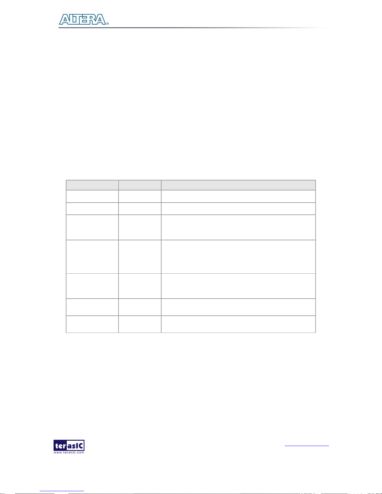
Setup Configure Mode Control DIP switch
The Configure Mode Control DIP switch (SW5) is provided to specify the configuration mode of the
FPGA. As currently only one mode is supported, please set all positions as shown in 99H99HFigure 2-3.
Page 13
TR5 User Manual
www.terasic.com
July 27, 2017
13
Figure 2-3 4-Position DIP switch for Configure Mode
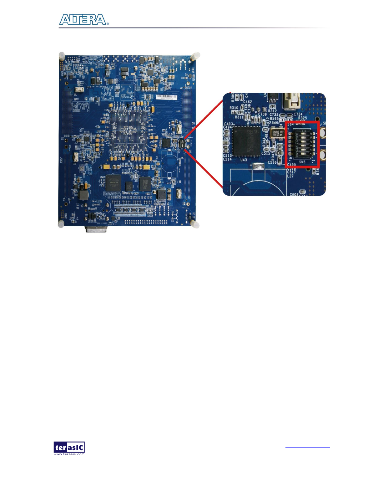
Select Flash Image for Configuration
The Image Select DIP switch (SW4) is provided to specify the image for configuration of the FPGA.
Setting SW4 to high (‘0’) specifies the default factory image to be loaded, setting SW4 to low (‘1’)
specifies the TR5 to load a user-defined image, as shown in 101H101HFigure 2-4.
Page 14
TR5 User Manual
www.terasic.com
July 27, 2017
14
Figure 2-4 2-position DIP switch for Image Select
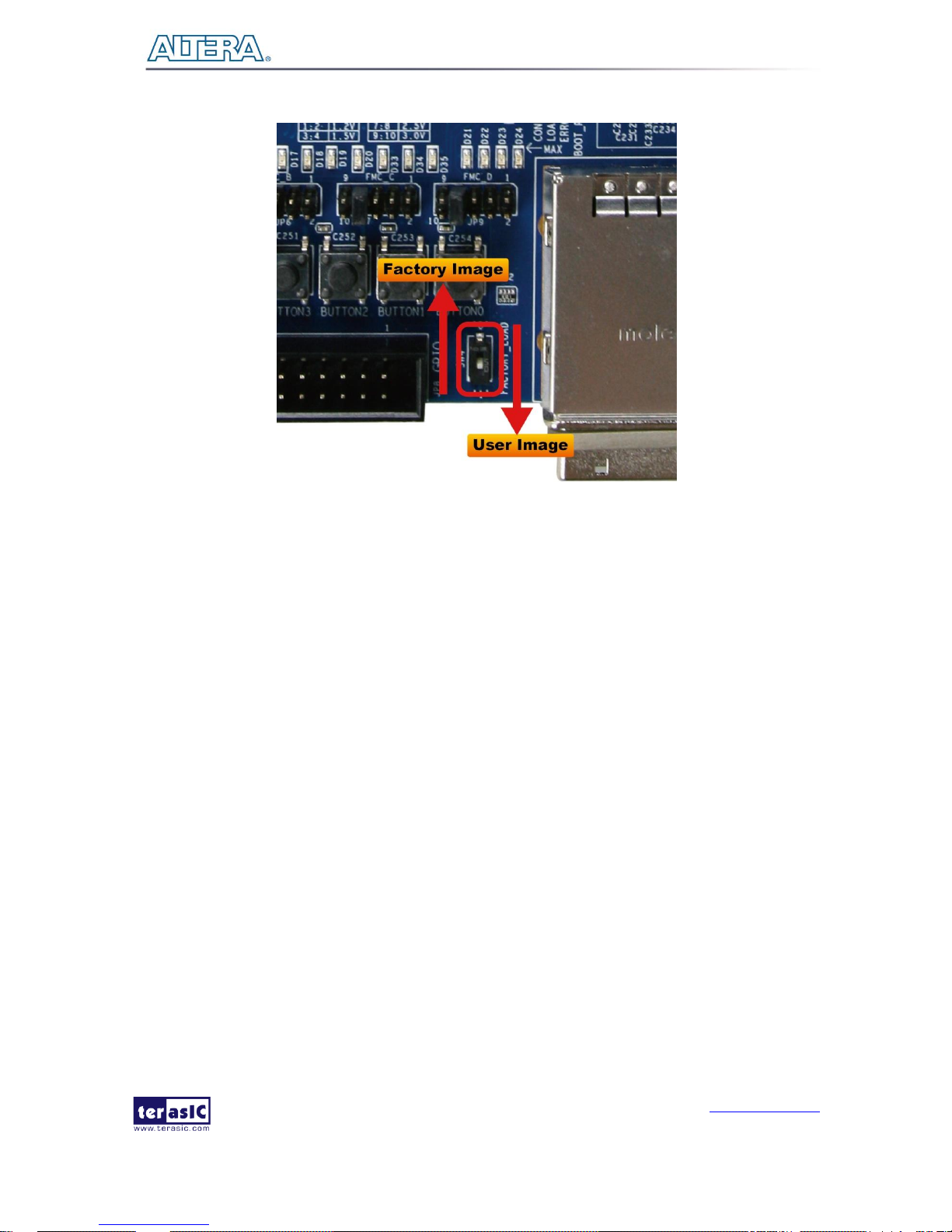
FMC VCCIO Voltage Setting Header
The I/O voltage of all the four FMC connectors is adjustable within 1.2/1.5/1.8/2.5/3.0V. For example,
user can adjust the I/O voltage to 2.5V to support LVDS differential I/O stand. The user can
independently control the voltage of FMCA~FMCD through JP5, JP6, JP7 and JP9. As shown in
Figure 2-5, make short circuit onto JP5 pin 7 and pin 8, the status of D12, D13 and D14 will be set
as “ON/OFF/ON” for representing the FMCA VCCIO is 2.5V. Table 2-2, Table 2-3, Table 2-4 and
Table 2-5 lists the voltage settings of the FMCA~FMCD VCCIO and their corresponding LED
display status.
Page 15
TR5 User Manual
www.terasic.com
July 27, 2017
15
Figure 2-5 FMC A VCCIO Voltage Setting to 2.5V
Table 2-2 FMC A VCCIO Voltage Setting
JP5 Setting
LED Status
FMC A VCCIO Voltage
D12
D13
D14
Short Pin 1 & 2
OFF
OFF
ON
1.2V
Short Pin 3 & 4
OFF
ON
OFF
1.5V
Short Pin 5 & 6
OFF
ON
ON
1.8V
Short Pin 7 & 8
ON
OFF
ON
2.5V(Default)
Short Pin 9 & 10
ON
ON
OFF
3.0V
Table 2-3 FMC B VCCIO Voltage Setting
JP6 Setting
LED Status
FMC B VCCIO Voltage
D15
D16
D17
Short Pin 1 & 2
OFF
OFF
ON
1.2V
Short Pin 3 & 4
OFF
ON
OFF
1.5V
Short Pin 5 & 6
OFF
ON
ON
1.8V
Short Pin 7 & 8
ON
OFF
ON
2.5V(Default)
Short Pin 9 & 10
ON
ON
OFF
3.0V
Page 16
TR5 User Manual
www.terasic.com
July 27, 2017
16
Table 2-4 FMC C VCCIO Voltage Setting
JP7 Setting
LED Status
FMC C VCCIO Voltage
D18
D19
D20
Short Pin 1 & 2
OFF
OFF
ON
1.2V
Short Pin 3 & 4
OFF
ON
OFF
1.5V
Short Pin 5 & 6
OFF
ON
ON
1.8V
Short Pin 7 & 8
ON
OFF
ON
2.5V(Default)
Short Pin 9 & 10
ON
ON
OFF
3.0V
Table 2-5 FMC D VCCIO Voltage Setting
JP9 Setting
LED Status
FMC D VCCIO Voltage
D33
D34
D35
Short Pin 1 & 2
OFF
OFF
ON
1.2V
Short Pin 3 & 4
OFF
ON
OFF
1.5V
Short Pin 5 & 6
OFF
ON
ON
1.8V
Short Pin 7 & 8
ON
OFF
ON
2.5V(Default)
Short Pin 9 & 10
ON
ON
OFF
3.0V
FMC JTAG Header
The TR5 supports individual JTAG interfaces on each FMC connector. This feature allows users to
extend the JTAG chain to FMC daughter cards. The JTAG signals on each FMC connector can be
removed or included in the active JTAG chain via 3-Pin header (See Figure 2-6). Table 2-6 lists the
setting of the headers and their associated interfaces. Note that if the JTAG interface on FMC
connector is enabled, make sure that the active JTAG chain must be a closed loop or the FPGA may
not be detected.
Page 17
TR5 User Manual
www.terasic.com
July 27, 2017
17
Figure 2-6 FMCC JTAG Header
Table 2-6 FMC JTAG Header Setting
Headers
Setting
Description
JP1
Short Pin 1 & 2
Disable FMCA JTAG
Short Pin 2 & 3
Enable FMCA JTAG
JP2
Short Pin 1 & 2
Disable FMCD JTAG
Short Pin 2 & 3
Enable FMCD JTAG
JP3
Short Pin 1 & 2
Disable FMCB JTAG
Short Pin 2 & 3
Enable FMCB JTAG
JP4
Short Pin 1 & 2
Disable FMCC JTAG
Short Pin 2 & 3
Enable FMCC JTAG
2.3 General User Input/Output
This section describes the user I/O interface to the FPGA.
User Defined Push-buttons
The FPGA board includes four user defined push-buttons that allow users to interact with the Stratix
V GX device. Each push-button provides a high logic level or a low logic level when it is not pressed
Page 18
TR5 User Manual
www.terasic.com
July 27, 2017
18
or pressed, respectively. 102H102HTable 2-7 lists the board references, signal names and their corresponding
Stratix V GX device pin numbers.
Table 2-7 Push-button Pin Assignments, Schematic Signal Names, and Functions
Board
Reference
Schematic
Signal Name
Description
I/O
Standard
Stratix V GX
Pin Number
BUTTON0
BUTTON0
High Logic Level when the button is
not pressed
1.5-V
PIN_BC7
BUTTON1
BUTTON1
1.5-V
PIN_BD7
BUTTON 2
BUTTON2
1.5-V
PIN_BB8
BUTTON 3
BUTTON3
1.5-V
PIN_BB9
User-Defined Slide Switch
There are four slide switches on the FPGA board to provide additional FPGA input control. When a
slide switch is in the DOWN position or the UPPER position, it provides a low logic level or a high
logic level to the Stratix V GX FPGA. The down position provides a low logic level and the upper
position provides a high logic level.
104H104HTable 2-8 lists the signal names and their corresponding Stratix V GX device pin numbers.
Table 2-8 Slide Switch Pin Assignments, Schematic Signal Names, and Functions
Board
Reference
Schematic
Signal Name
Description
I/O
Standard
Stratix V GX
Pin Number
SW0
SW0
High logic level when SW in the UPPER
position.
1.5-V
PIN_AT9
SW1
SW1
1.5-V
PIN_AU8
SW2
SW2
1.5-V
PIN_AK9
SW3
SW3
1.5-V
PIN_AL9
User-Defined LEDs
The FPGA board consists of four user-controllable LEDs to allow status and debugging signals to be
driven to the LEDs from the designs loaded into the Stratix V GX device. Each LED is driven directly
by the Stratix V GX FPGA. The LEDs are turned on or off when the associated pins are driven to a
low or high logic level, respectively. A list of the pin names on the FPGA that are connected to the
LEDs is given in 105H105HTable 2-9.
Page 19
TR5 User Manual
www.terasic.com
July 27, 2017
19
Table 2-9 User LEDs Pin Assignments, Schematic Signal Names, and Functions
Board
Reference
Schematic
Signal Name
Description
I/O
Standard
Stratix V GX
Pin Number
LED0
LED0
Driving a logic 0 on the I/O port turns the LED
ON.
Driving a logic 1 on the I/O port turns the LED
OFF.
1.5-V
PIN_AT32
LED1
LED1
1.5-V
PIN_BA31
LED2
LED2
1.5-V
PIN_AN27
LED3
LED3
1.5-V
PIN_AH27
UART-To-USB
The UART is designed to perform communication between the board and the PC, allowing a
transmission speed of up to 3Mbps. This interface wouldn’t support HW flow control signals. The
physical interface is done using UART-USB on-board bridge from a FT232R chip and connects to
the host using a USB Type-B connector. For detailed information on how to use the transceiver, please
refer to the datasheet, which is available on the manufacturer’s website, or under the
Datasheets\FT232 folder on the Kit System CD. Figure 2-7 shows the related schematics, and Table
2-10 lists the UART pin assignments, signal names and functions.
Figure 2-7 Connection between UART-To-USB and Stratix V GX FPGA
Table 2-10 UART-To-USB Pin Assignments, Schematic Signal Names, and Functions
Board
Reference
Schematic
Signal
Name
Description
I/O Standard
Stratix V
GX Pin
Number
UART_TX
UART_TX
Uart TX output from FPGA
1.2/1.5/1.8/2.5/3.0-
PIN_T26
Page 20
TR5 User Manual
www.terasic.com
July 27, 2017
20
V
UART_RX
UART_RX
Uart RX input to FPGA
1.2/1.5/1.8/2.5/3.0V
PIN_T25
Micro SD-Card
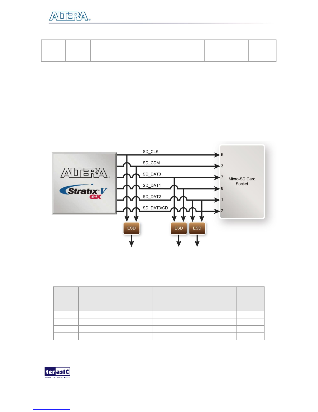
The development board supports Micro SD card interface using 4 data lines. Figure 2-8 shows the
related signals connections between the SD Card and Stratix V GX FPGA. Table 2-11 lists all the
associated pins
Figure 2-8 Connection between the SD Card Socket and Stratix V GX FPGA
Table 2-11 Micro SD Card Pin Assignments, Schematic Signal Names, and Functions
Schematic
Signal
Name
Description
I/O Standard
Stratix V
GX Pin
Number
SD_CLK
Serial Clock
1.5-V
PIN_BB39
SD_CMD
Command, Response
1.5-V
PIN_BA36
SD_DAT0
Serial Data 0
1.5-V
PIN_AV37
SD_DAT1
Serial Data 1
1.5-V
PIN_AY37
Page 21
TR5 User Manual
www.terasic.com
July 27, 2017
21
SD_DAT2
Serial Data 2
1.5-V
PIN_BB36
SD_DAT3
Serial Data 3
1.5-V
PIN_AW37
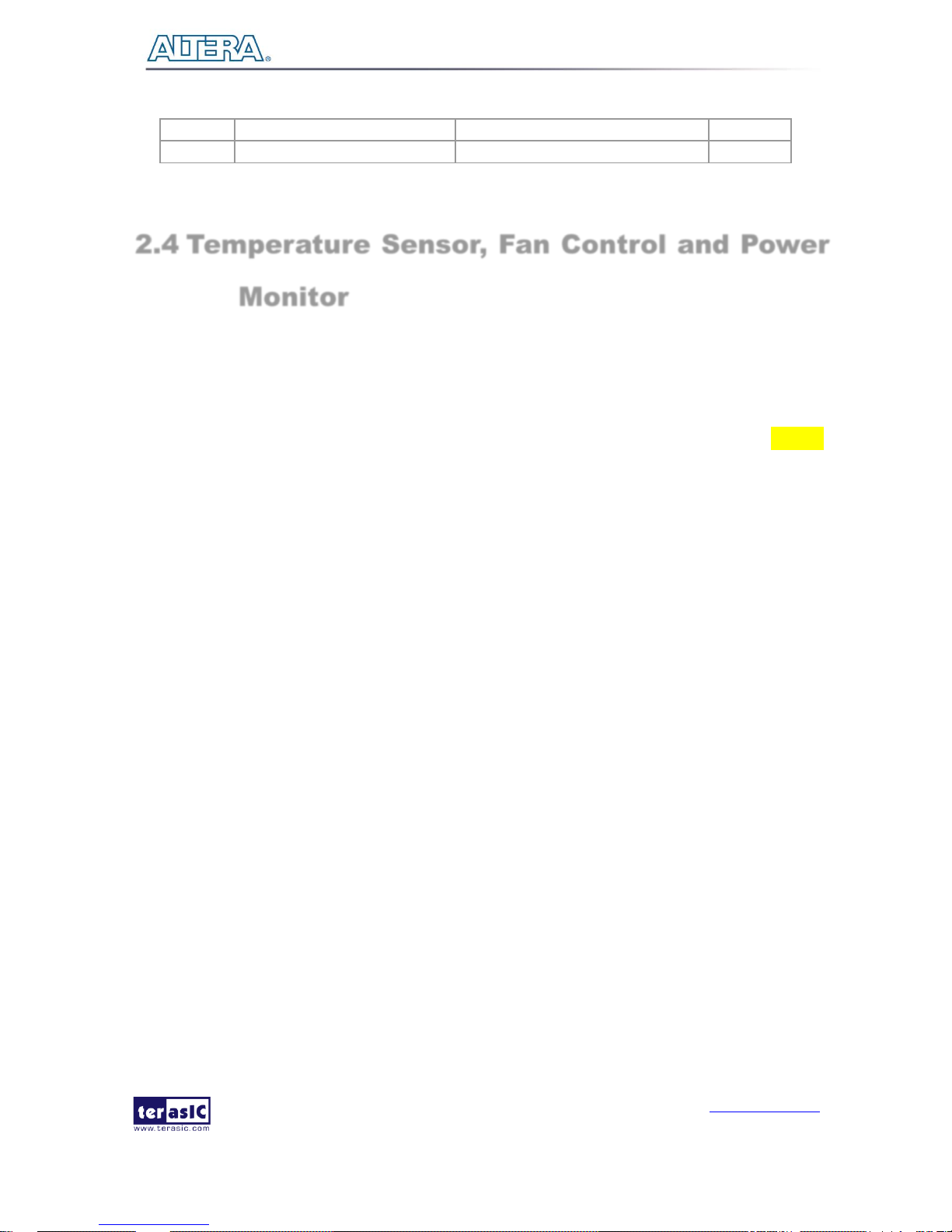
2.4 Temperature Sensor, Fan Control and Power
Monitor
The FPGA board is equipped with a temperature sensor, MAX1619, which provides temperature
sensing and over-temperature alert. These functions are accomplished by connecting the temperature
sensor to the internal temperature sensing diode of the Stratix V GX device. The temperature status
and alarm threshold registers of the temperature sensor can be programmed by a two-wire SMBus,
which is connected to the Stratix V GX FPGA. In addition, the 7-bit POR slave address for this sensor
is set to ‘0011000b’.
A 3-pin +12V fan located on J12 of the FPGA board is intended to reduce the temperature of the
FPGA. The board is equipped with a Fan-Speed regulator and monitor MAX6650 with an I2C/SMBus
interfaces, Users regulate and monitor the speed of fan depending on the measured system
temperature.
The TR5 has implemented a power monitor chip to monitor the board input power voltage and current.
Figure 2-9 shows the connection between the power monitor chip and the Stratix V GX FPGA. The
power monitor chip monitors both shunt voltage drops and board input power voltage allows user to
monitor the total board power consumption. Programmable calibration value, conversion times, and
averaging, combined with an internal multiplier, enable direct readouts of current in amperes and
power in watts. Note that, the temperature sensor, fan control and power monitor share the same
I2C/SMBUS.
Page 22
TR5 User Manual
www.terasic.com
July 27, 2017
22
Figure 2-9 Connections between the temperature sensor/fan control/power monitor and the
Stratix V GX FPGA
Table 2-12 Temperature Sensor and Fan Speed Control Pin Assignments, Schematic Signal
Names, and Functions
Schematic
Signal Name
Description
I/O Standard
Stratix V GX Pin
Number
TEMPDIODEp
Positive pin of temperature diode
in Stratix V
-
PIN_P6
TEMPDIODEn
Negative pin of temperature diode
in Stratix V
-
PIN_P7
FPGA_I2C_SCL
SMBus clock
1.5-V
PIN_AN11
FPGA_I2C_SDA
SMBus data
1.5-V
PIN_AP9
TEMP_OVERT_n
SMBus alert (interrupt)
1.5-V
PIN_AR9
TEMP_INT_n
SMBus alert (interrupt)
1.5-V
PIN_AT8
POWER_MONITOR_ALERT
Active-high ALERT input
1.5-V
PIN_AY9
FAN_ALERT_n
Active-low ALERT input
1.5-V
PIN_AM11
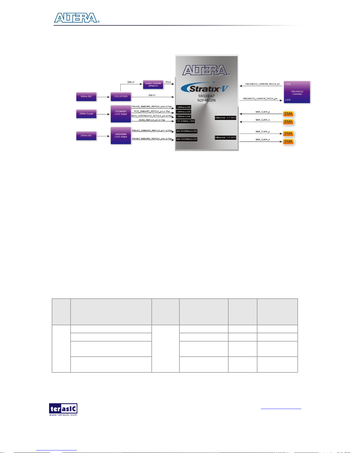
2.5 Clock Circuit
The development board includes one 50 MHz and two programmable clock generators. Figure 2-10
shows the default frequencies of on-board all external clocks going to the Stratix V GX FPGA.
Page 23
TR5 User Manual
www.terasic.com
July 27, 2017
23
Figure 2-10 Clock circuit of the FPGA Board
A clock buffer is used to duplicate the 50 MHz oscillator, so there are seven 50MHz clocks fed into
seven different FPGA banks. The two programming clock generators are low-jitter oscillators which
are used to provide special and high quality clock signals for high-speed transceivers and high
bandwidth memory. Through I2C serial interface, the clock generator controllers in the Stratix V GX
FPGA can be used to program the CDCM6208 and LMK04096B to generate PCIe, SATA and high
bandwidth memory reference clocks respectively. Two SMA connectors and Four FMC connectors
provide external differential clock input(s) and clock output(s) respectively.
112H112HTable 2-9 lists the clock source, signal names, default frequency and their corresponding Stratix V
GX device pin numbers.
Table 2-9 Clock Source, Signal Name, Default Frequency, Pin Assignments and Functions
Source
Schematic
Signal Name
Default
Frequency
I/O Standard
Stratix V
GX Pin
Number
Application
Y1
CLK_50_B3B
50.0 MHz
1.5-V
PIN_AW35
CLK_50_B4A
1.5-V
PIN_AP10
CLK_50_B4D
1.2/1.5/1.8/2.5/3.0V
PIN_AY18
CLK_50_B7A
1.2/1.5/1.8/2.5/3.0V
PIN_M8
Page 24
TR5 User Manual
www.terasic.com
July 27, 2017
24
CLK_50_B7D
1.2/1.5/1.8/2.5/3.0V
PIN_J18
CLK_50_B8A
1.2/1.5/1.8/2.5/3.0V
PIN_R36
CLK_50_B8D
1.2/1.5/1.8/2.5/3.0V
PIN_R25
J3
SMA_CLKIN_p
User
Defined
1.5-V
PIN_BC8
External Clock
Input
J4
SMA_CLKIN_n
User
Defined
1.5-V
PIN_BD8
Clock Output
J1
SMA_CLKOUT_p
User
Defined
1.5-V
PIN_AV8
J2
SMA_CLKOUT_n
User
Defined
1.5-V
PIN_AW9
U21
FMCA_ONBOARD_REFCLK_p0
125 MHz
LVDS
PIN_Y38
FMCA port xcvr
reference clock
FMCD_ONBOARD_REFCLK_p0
125 MHz
LVDS
PIN_Y7
FMCD port xcvr
reference clock
PCIE_ONBOARD_REFCLK_p
100 MHz
LVDS
PIN_AH39
PCIe reference
clock
SATA_DEVICE_REFCLK_p
150 MHz
LVDS
PIN_AK7
SATA Device
reference clock
SATA_HOST_REFCLK_p
150 MHz
PIN_BB33
SATA Host
reference clock
DDR3_REFCLK_p
133.333
MHz
DDR3
reference clock
U43
FMCA_ONBOARD_REFCLK_p1
644.53125
MHz
LVDS
PIN_T38
FMCA port xcvr
reference clock
FMCD_ONBOARD_REFCLK_p1
644.53125
MHz
LVDS
PIN_T7
FMCD port xcvr
reference clock
FMCC_ONBOARD_REFCLK_p0
644.53125
MHz
LVDS
PIN_AD39
FMCB port xcvr
reference clock
FMCC_ONBOARD_REFCLK_p1
644.53125
MHz
LVDS
PIN_AD6
FMCC port xcvr
reference clock
113H113HTable 2-10 lists the programmable oscillator control pins, signal names, I/O standard and their
corresponding Stratix V GX device pin numbers.
Table 2-10 Programmable oscillator control pin, Signal Name, I/O standard, Pin
Assignments and Descriptions
Page 25
TR5 User Manual
www.terasic.com
July 27, 2017
25
Programmable
Oscillator
Schematic
Signal Name
I/O Standard
Stratix V GX Pin
Number
Description
CDCM6208
(U21)
CLOCK_SCL
2.5-V
PIN_AR25
I2C bus, connected
with CDCM6208
CLOCK_SDA
2.5-V
PIN_BC25
LMK04906B
(U43)
LMK04906_CLK
2.5-V
PIN_AT24
I2C bus master output
only, connected with
LMK04096B
LMK04906_DATAIN
2.5-V
PIN_BD25
LMK04906_DATAOUT
1.5-V
PIN_BC29
I2C bus master input
signal
LMK04906_LE
1.5-V
PIN_AT33
LMK04096B PLL
locked signal
2.6 FLASH and SSRAM Memory
The development board has a 1G bit CFI-compatible synchronous flash device for non-volatile
storage of FPGA configuration data, user application data, and user code space, and a 2M byte ZBT
SSRAM for data Cache.
The flash has a 16-bit data bus and allow for FPP x16 configuration. This device is part of the
shared flash and MAX (FM) bus, which connects to the flash memory and MAX II CPLD
(EPM2210) System Controller. The SSRAM also has a 16-bit data bus and share address and data
bus with the flash. 1Figure 2-11 shows the connections between the Flash, SSRAM, MAX and
Stratix V GX FPGA.
Page 26

TR5 User Manual
www.terasic.com
July 27, 2017
26
Figure 2-11 Connection between the Flash, Max and Stratix V GX FPGA
117H117HTable 2-11 lists the flash pin assignments, signal names, and functions.
Table 2-13 Flash Memory Pin Assignments, Schematic Signal Names, and Functions
Schematic
Signal Name
Description
I/O Standard
Stratix V GX
Pin Number
FSM_A1
Address bus
2.5V
PIN_AE11
FSM_A2
Address bus
2.5V
PIN_AD14
FSM_A3
Address bus
2.5V
PIN_AE14
FSM_A4
Address bus
2.5V
PIN_AE10
FSM_A5
Address bus
2.5V
PIN_AF10
FSM_A6
Address bus
2.5V
PIN_AE12
FSM_A7
Address bus
2.5V
PIN_AF11
FSM_A8
Address bus
2.5V
PIN_AG13
FSM_A9
Address bus
2.5V
PIN_AJ10
FSM_A10
Address bus
2.5V
PIN_AF13
FSM_A11
Address bus
2.5V
PIN_AE13
FSM_A12
Address bus
2.5V
PIN_AJ11
FSM_A13
Address bus
2.5V
PIN_BD11
FSM_A14
Address bus
2.5V
PIN_AW10
FSM_A15
Address bus
2.5V
PIN_AF14
Page 27
TR5 User Manual
www.terasic.com
July 27, 2017
27
FSM_A16
Address bus
2.5V
PIN_AY12
FSM_A17
Address bus
2.5V
PIN_AY10
FSM_A18
Address bus
2.5V
PIN_BD10
FSM_A19
Address bus
2.5V
PIN_BB12
FSM_A20
Address bus
2.5V
PIN_BA12
FSM_A21
Address bus
2.5V
PIN_BA10
FSM_A22
Address bus
2.5V
PIN_BC11
FSM_A23
Address bus
2.5V
PIN_AE9
FSM_A24
Address bus
2.5V
PIN_AW11
FSM_A25
Address bus
2.5V
PIN_BC10
FSM_A26
Address bus
2.5V
PIN_BB11
FSM_D0
Data bus
2.5V
PIN_AG10
FSM_D1
Data bus
2.5V
PIN_AH10
FSM_D2
Data bus
2.5V
PIN_AG11
FSM_D3
Data bus
2.5V
PIN_AK12
FSM_D4
Data bus
2.5V
PIN_AV10
FSM_D5
Data bus
2.5V
PIN_AR12
FSM_D6
Data bus
2.5V
PIN_AL12
FSM_D7
Data bus
2.5V
PIN_AR13
FSM_D8
Data bus
2.5V
PIN_AG9
FSM_D9
Data bus
2.5V
PIN_AH12
FSM_D10
Data bus
2.5V
PIN_AG12
FSM_D11
Data bus
2.5V
PIN_AL11
FSM_D12
Data bus
2.5V
PIN_AN12
FSM_D13
Data bus
2.5V
PIN_AU9
FSM_D14
Data bus
2.5V
PIN_AM13
FSM_D15
Data bus
2.5V
PIN_AJ12
FLASH_CLK
Flash Clock
2.5V
PIN_AU11
FLASH_RESET_n
Flash Reset, active low
2.5V
PIN_AV25
FLASH_CE_n
Flash Chip enable,active low
2.5V
PIN_AU24
FLASH_OE_n
Flash Output enable, active
low
2.5V
PIN_AP12
FLASH_WE_n
Flash Write enable, active low
2.5V
PIN_AT12
FLASH_ADV_n
Flash Address valid, active
low
2.5V
PIN_BD26
FLASH_RDY_BSY_n
Flash ready output
2.5V
PIN_AU25
SSRAM_CLK
SSRAM Clock
2.5V
PIN_AP13
SSRAM_CKE_n
SSRAM Clock enable, active
low
2.5V
PIN_AW24
SSRAM_CE_n
SSRAM Chip enable, active
low
2.5V
PIN_AP24
Page 28
TR5 User Manual
www.terasic.com
July 27, 2017
28
SSRAM_WE_n
Flash Write enable, active low
2.5V
PIN_AV11
SSRAM_OE_n
Flash output enable, active
low
2.5V
PIN_AU10
SSRAM_ADV
Flash Address valid, active
high
2.5V
PIN_BC26
SSRAM_BWA_n
SSRAM Byte Write enable
2.5V
PIN_AY25
SSRAM_BWB_n
SSRAM Byte Write enable
2.5V
PIN_BA24
FLASH_CLK
Clock
2.5V
PIN_T9
FLASH_RESET_n
Reset
2.5V
PIN_C17
FLASH_CE_n
Chip enable of of flash-0
2.5V
PIN_H10
Chip enable of of flash-1
2.5V
PIN_N16
FLASH_OE_n
Output enable
2.5V
PIN_C16
FLASH_WE_n
Write enable
2.5V
PIN_U10
FLASH_ADV_n
Address valid
2.5V
PIN_H7
FLASH_RDY_BSY_n
Ready of flash-0
2.5V
PIN_J8
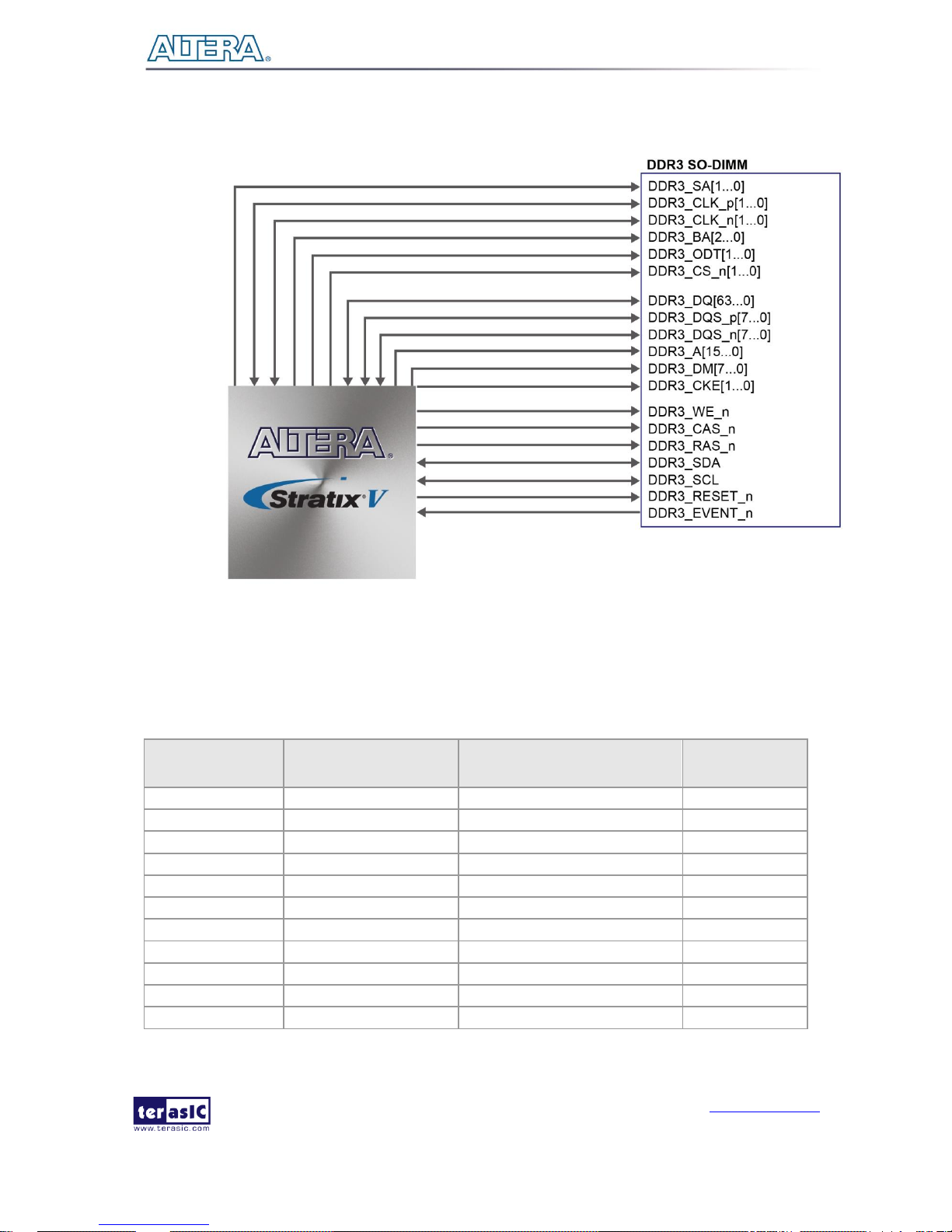
2.7 DDR3 SO-DIMM
The development board supports DDR3 SDRAM SO-DIMM. The DDR3 SODIMM socket is wired
to support a maximum capacity of 8GB with a 64-bit data bus. Using differential DQS signaling for
the DDR3 SDRAM interfaces, it is capable of running at up to 800MHz memory clock for a maximum
theoretical bandwidth up to 95.4Gbps. Figure 2-12 shows the connections between the DDR3
SDRAM SO-DIMMs and Stratix V GX FPGA.
Page 29
TR5 User Manual
www.terasic.com
July 27, 2017
29
Figure 2-12 Connection between the DDR3 and Stratix V GX FPGA
The pin assignments for DDR3 SDRAM SO-DIMM are listed in Table 2-14.
Table 2-14 DDR3 Pin Assignments, Schematic Signal Names, and Functions
Schematic
Signal Name
Description
I/O Standard
Stratix V GX Pin
Number
DDR3_DQ0
Data [0]
SSTL-15 Class I
PIN_AH31
DDR3_DQ1
Data [1]
SSTL-15 Class I
PIN_AJ31
DDR3_DQ2
Data [2]
SSTL-15 Class I
PIN_AN30
DDR3_DQ3
Data [3]
SSTL-15 Class I
PIN_AP30
DDR3_DQ4
Data [4]
SSTL-15 Class I
PIN_AH30
DDR3_DQ5
Data [5]
SSTL-15 Class I
PIN_AJ30
DDR3_DQ6
Data [6]
SSTL-15 Class I
PIN_AR30
DDR3_DQ7
Data [7]
SSTL-15 Class I
PIN_AT30
DDR3_DQ8
Data [8]
SSTL-15 Class I
PIN_AM29
DDR3_DQ9
Data [9]
SSTL-15 Class I
PIN_AN28
DDR3_DQ10
Data [10]
SSTL-15 Class I
PIN_AP28
Page 30
TR5 User Manual
www.terasic.com
July 27, 2017
30
DDR3_DQ11
Data [11]
SSTL-15 Class I
PIN_AR29
DDR3_DQ12
Data [12]
SSTL-15 Class I
PIN_AU31
DDR3_DQ13
Data [13]
SSTL-15 Class I
PIN_AV32
DDR3_DQ14
Data [14]
SSTL-15 Class I
PIN_AW32
DDR3_DQ15
Data [15]
SSTL-15 Class I
PIN_AV31
DDR3_DQ16
Data [16]
SSTL-15 Class I
PIN_AF28
DDR3_DQ17
Data [17]
SSTL-15 Class I
PIN_AF29
DDR3_DQ18
Data [18]
SSTL-15 Class I
PIN_AG30
DDR3_DQ19
Data [19]
SSTL-15 Class I
PIN_AG29
DDR3_DQ20
Data [20]
SSTL-15 Class I
PIN_AG28
DDR3_DQ21
Data [21]
SSTL-15 Class I
PIN_AG27
DDR3_DQ22
Data [22]
SSTL-15 Class I
PIN_AG26
DDR3_DQ23
Data [23]
SSTL-15 Class I
PIN_AG25
DDR3_DQ24
Data [24]
SSTL-15 Class I
PIN_BC31
DDR3_DQ25
Data [25]
SSTL-15 Class I
PIN_BC32
DDR3_DQ26
Data [26]
SSTL-15 Class I
PIN_BB30
DDR3_DQ27
Data [27]
SSTL-15 Class I
PIN_BD31
DDR3_DQ28
Data [28]
SSTL-15 Class I
PIN_BD32
DDR3_DQ29
Data [29]
SSTL-15 Class I
PIN_BA30
DDR3_DQ30
Data [30]
SSTL-15 Class I
PIN_AY31
DDR3_DQ31
Data [31]
SSTL-15 Class I
PIN_AW30
DDR3_DQ32
Data [32]
SSTL-15 Class I
PIN_BB29
DDR3_DQ33
Data [33]
SSTL-15 Class I
PIN_BB27
DDR3_DQ34
Data [34]
SSTL-15 Class I
PIN_BA27
DDR3_DQ35
Data [35]
SSTL-15 Class I
PIN_AW27
DDR3_DQ36
Data [36]
SSTL-15 Class I
PIN_AY28
DDR3_DQ37
Data [37]
SSTL-15 Class I
PIN_BA28
DDR3_DQ38
Data [38]
SSTL-15 Class I
PIN_AW29
DDR3_DQ39
Data [39]
SSTL-15 Class I
PIN_AY27
DDR3_DQ40
Data [40]
SSTL-15 Class I
PIN_AT27
DDR3_DQ41
Data [41]
SSTL-15 Class I
PIN_AN25
DDR3_DQ42
Data [42]
SSTL-15 Class I
PIN_AM25
DDR3_DQ43
Data [43]
SSTL-15 Class I
PIN_AL25
DDR3_DQ44
Data [44]
SSTL-15 Class I
PIN_AW26
DDR3_DQ45
Data [45]
SSTL-15 Class I
PIN_AV26
DDR3_DQ46
Data [46]
SSTL-15 Class I
PIN_AU27
DDR3_DQ47
Data [47]
SSTL-15 Class I
PIN_AM26
DDR3_DQ48
Data [48]
SSTL-15 Class I
PIN_AU28
DDR3_DQ49
Data [49]
SSTL-15 Class I
PIN_AU29
DDR3_DQ50
Data [50]
SSTL-15 Class I
PIN_AM28
DDR3_DQ51
Data [51]
SSTL-15 Class I
PIN_AL27
Page 31

TR5 User Manual
www.terasic.com
July 27, 2017
31
DDR3_DQ52
Data [52]
SSTL-15 Class I
PIN_AV28
DDR3_DQ53
Data [53]
SSTL-15 Class I
PIN_AV29
DDR3_DQ54
Data [54]
SSTL-15 Class I
PIN_AL28
DDR3_DQ55
Data [55]
SSTL-15 Class I
PIN_AK27
DDR3_DQ56
Data [56]
SSTL-15 Class I
PIN_AK24
DDR3_DQ57
Data [57]
SSTL-15 Class I
PIN_AJ24
DDR3_DQ58
Data [58]
SSTL-15 Class I
PIN_AH24
DDR3_DQ59
Data [59]
SSTL-15 Class I
PIN_AH25
DDR3_DQ60
Data [60]
SSTL-15 Class I
PIN_AH28
DDR3_DQ61
Data [61]
SSTL-15 Class I
PIN_AJ28
DDR3_DQ62
Data [62]
SSTL-15 Class I
PIN_AL26
DDR3_DQ63
Data [63]
SSTL-15 Class I
PIN_AK26
DDR3_DQS0
Data Strobe p[0]
Differential 1.5-V SSTL Class I
PIN_AL30
DDR3_DQS_n0
Data Strobe n[0]
Differential 1.5-V SSTL Class I
PIN_AL31
DDR3_DQS1
Data Strobe p[1]
Differential 1.5-V SSTL Class I
PIN_AK30
DDR3_DQS_n1
Data Strobe n[1]
Differential 1.5-V SSTL Class I
PIN_AL29
DDR3_DQS2
Data Strobe p[2]
Differential 1.5-V SSTL Class I
PIN_AE27
DDR3_DQS_n2
Data Strobe n[2]
Differential 1.5-V SSTL Class I
PIN_AE28
DDR3_DQS3
Data Strobe p[3]
Differential 1.5-V SSTL Class I
PIN_AY30
DDR3_DQS_n3
Data Strobe n[4]
Differential 1.5-V SSTL Class I
PIN_BA29
DDR3_DQS4
Data Strobe p[4]
Differential 1.5-V SSTL Class I
PIN_BC28
DDR3_DQS_n4
Data Strobe n[4]
Differential 1.5-V SSTL Class I
PIN_BD28
DDR3_DQS5
Data Strobe p[5]
Differential 1.5-V SSTL Class I
PIN_AT26
DDR3_DQS_n5
Data Strobe n[5]
Differential 1.5-V SSTL Class I
PIN_AU26
DDR3_DQS6
Data Strobe p[6]
Differential 1.5-V SSTL Class I
PIN_AR27
DDR3_DQS_n6
Data Strobe n[6]
Differential 1.5-V SSTL Class I
PIN_AR28
DDR3_DQS7
Data Strobe p[7]
Differential 1.5-V SSTL Class I
PIN_AJ25
DDR3_DQS_n7
Data Strobe n[7]
Differential 1.5-V SSTL Class I
PIN_AJ26
DDR3_DM0
Data Mask [0]
SSTL-15 Class I
PIN_AU32
DDR3_DM1
Data Mask [1]
SSTL-15 Class I
PIN_AU30
DDR3_DM2
Data Mask [2]
SSTL-15 Class I
PIN_AK29
DDR3_DM3
Data Mask [3]
SSTL-15 Class I
PIN_BB32
DDR3_DM4
Data Mask [4]
SSTL-15 Class I
PIN_BD29
DDR3_DM5
Data Mask [5]
SSTL-15 Class I
PIN_AR26
DDR3_DM6
Data Mask [6]
SSTL-15 Class I
PIN_AP27
DDR3_DM7
Data Mask [7]
SSTL-15 Class I
PIN_AJ27
DDR3_A0
Address [0]
SSTL-15 Class I
PIN_AM32
DDR3_A1
Address [1]
SSTL-15 Class I
PIN_AF31
DDR3_A2
Address [2]
SSTL-15 Class I
PIN_AJ33
DDR3_A3
Address [3]
SSTL-15 Class I
PIN_AE31
DDR3_A4
Address [4]
SSTL-15 Class I
PIN_AP33
Page 32

TR5 User Manual
www.terasic.com
July 27, 2017
32
DDR3_A5
Address [5]
SSTL-15 Class I
PIN_AG32
DDR3_A6
Address [6]
SSTL-15 Class I
PIN_AN33
DDR3_A7
Address [7]
SSTL-15 Class I
PIN_AK33
DDR3_A8
Address [8]
SSTL-15 Class I
PIN_AF32
DDR3_A9
Address [9]
SSTL-15 Class I
PIN_AH33
DDR3_A10
Address [10]
SSTL-15 Class I
PIN_AE30
DDR3_A11
Address [11]
SSTL-15 Class I
PIN_BA33
DDR3_A12
Address [12]
SSTL-15 Class I
PIN_AG33
DDR3_A13
Address [13]
SSTL-15 Class I
PIN_AD32
DDR3_A14
Address [14]
SSTL-15 Class I
PIN_BA34
DDR3_A15
Address [15]
SSTL-15 Class I
PIN_AY33
DDR3_RAS_n
Row Address Strobe
SSTL-15 Class I
PIN_AJ32
DDR3_CAS_n
Column Address Strobe
SSTL-15 Class I
PIN_AE33
DDR3_BA0
Bank Address [0]
SSTL-15 Class I
PIN_AE29
DDR3_BA1
Bank Address [1]
SSTL-15 Class I
PIN_AK32
DDR3_BA2
Bank Address [2]
SSTL-15 Class I
PIN_AE34
DDR3_CK0
Clock p0
Differential 1.5-V SSTL Class I
PIN_AR31
DDR3_CK_n0
Clock n0
Differential 1.5-V SSTL Class I
PIN_AR32
DDR3_CK1
Clock p1
Differential 1.5-V SSTL Class I
PIN_AV34
DDR3_CK_n1
Clock n1
Differential 1.5-V SSTL Class I
PIN_AW33
DDR3_CKE0
Clock Enable pin 0
SSTL-15 Class I
PIN_AF34
DDR3_CKE1
Clock Enable pin 1
SSTL-15 Class I
PIN_AY34
DDR3_ODT0
On Die Termination[0]
SSTL-15 Class I
PIN_AN31
DDR3_ODT1
On Die Termination[1]
SSTL-15 Class I
PIN_AM31
DDR3_WE_n
Write Enable
SSTL-15 Class I
PIN_AE32
DDR3_CS_n0
Chip Select [0]
SSTL-15 Class I
PIN_AP31
DDR3_CS_n1
Chip Select [1]
SSTL-15 Class I
PIN_AD33
DDR3_RESET_n
Chip Reset
SSTL-15 Class I
PIN_AR33
DDR3_EVENT_n
Chip Temperature Event
SSTL-15 Class I
PIN_AU35
DDR3_SDA
Chip I2C Serial Clock
1.5V
PIN_AJ29
DDR3_SCL
Chip I2C Serial Data Bus
1.5V
PIN_AT29
2.8 FMC Connectors
The FPGA Mezzanine Card (FMC) interface provides a mechanism to extend the peripheral-set of an
FPGA host board by means of add-on daughter cards, which can address today’s high speed signaling
requirements as well as low-speed device interface support. The FMC interfaces support JTAG, clock
Page 33

TR5 User Manual
www.terasic.com
July 27, 2017
33
outputs and inputs, high-speed serial I/O (transceivers), and single-ended or differential signaling.
The detailed specifications of the FMC connectors are described below:
4 FMC Connector
There are four FMC connectors on the TR5 board are: FMCA, FMCB, FMCC, FMCD. Both FMCA
and FMCD are High Pin Count (HPC) size of connectors and FMCB and FMCC are Low Pin Count
(LPC) size of connectors (See Figure 2-12). The HPC connector on TR5 board can provides 172
user-define, single-ended signals (include clock signals) and 10 serial transceiver pairs (See Figure
2-14). The LPC connector can provides 76 user-define, single-ended signals (include clock signals)
and 1 serial transceiver pairs (See Figure 2-15). The HPC and LPC connectors use the same
mechanical connector. The only difference is which signals are actually populated. Thus, cards with
LPC connectors can be plugged into HPC sites. Please note that some standard FMC cards may not
work with TR5 due to unidirectional LVDS due to Stratix V device.
Page 34

TR5 User Manual
www.terasic.com
July 27, 2017
34
Figure 2-13 FMC connectors on TR5 board
Figure 2-14 Pin-Out of the high pin count FMC connector
Page 35

TR5 User Manual
www.terasic.com
July 27, 2017
35
Figure 2-15 Pin-Out of the low pin count FMC connector
Clock Interface
Due to the limitation of the FPGA clock input pin numbers, not all the FMC ports have same clock
interface.
Page 36

TR5 User Manual
www.terasic.com
July 27, 2017
36
Table 2-15 shows the FPGA dedicated clock input pin placement on each FMC port.
Page 37

TR5 User Manual
www.terasic.com
July 27, 2017
37
Table 2-15 FMC clock interface distribution
FMC Clock in/out pin
name
FPGA Clock Input Pin Placement
FMCA
FMCB
FMCC
FMCD
CLK0_M2C_P
I/O
CLK22p
I/O
I/O
CLK0_M2C_N
I/O
CLK22n
I/O
I/O
CLK1_M2C_P
I/O
CLK23p
I/O
CLK15p
CLK1_M2C_N
I/O
CLK23n
I/O
CLK15n
HA01_P_CC
CLK17p
N/A
N/A
CLK14p
HA01_N_CC
CLK17n
N/A
N/A
CLK14n
LA01_P_CC
CLK19p
CLK21p
CLK7p
CLK13p
LA01_N_CC
CLK19n
CLK21n
CLK7n
CLK13n
Please note that, all the dedicated clock pin of the FPGA are connected to external termination
resistors (See Figure 2-16 ). IF users want to us these I/O as single-end standard, pleaser remove
these resistors.
Figure 2-16 Termination resistors on FMC clock I/Os
Page 38

TR5 User Manual
www.terasic.com
July 27, 2017
38
Power Supply
The TR5 board provides 12V, 3.3V and VCCIO_FMC power through FMC ports. Table 2-16
indicates the maximum power consumption for all FMC ports. Please note that this table shows the
total max current limit for all six ports, not just for one.
Also, the 12V DC power supplies from the FMC ports have fuses for protection. Users who don’t
need the power from the FMC can remove these fuses to cut the power on connector.
CAUTION. Before powering on the TR5 board with a daughter card, please check to see if there is
a short circuit between the power pins and FPGA I/O.
Table 2-16 Power Supply of the FMC
Supplied Voltage
Max. Current Limit
12V
3A
3.3V
3A
VCCIO_FMC
FMCA : 12A ; FMCB/FMCC/FMCD : 6A
Adjustable I/O Standards
The FPGA I/O standards of the FMC ports can be adjusted by configuring the header position. Each
port can be individually adjusted to 1.5V, 1.8V, 2.5V or 3.0V via jumpers on the TR5 board. For
detailed setting, please refer to Section 2.2.
JTAG Chain on FMC
Figure 2-17 shows the JTAG chain loop of the TR5 board. The JTAG interface on the FMC connectors
can be activated through four 3-pin headers. For detailed setting, please refer to Section 2.2.
Page 39

TR5 User Manual
www.terasic.com
July 27, 2017
39
Figure 2-17 JTAG Chain for a Standalone TR5
Component Information of the FMC Connector
Table 2-17 shows the manufacture and part numbers of the FMC connector.
Table 2-17 Component information of the FMC connector
Connector Type
Manufacturer
Part Number
Female
(For Mother Board)
High Pin Count(HPC)
SAMTEC
ASP-134486-01
Low Pin Count(LPC)
SAMTEC
ASP-134603-01
Male
High Pin Count(HPC)
SAMTEC
ASP-134488-01
Page 40

TR5 User Manual
www.terasic.com
July 27, 2017
40
(For Daughter Board)
Low Pin Count(LPC)
SAMTEC
ASP-134604-01
2.9 SATA
The two Serial ATA (SATA) ports are available on the FPGA development board which are computer
bus standard with a primary function of transferring data between the motherboard and mass storage
devices (such as hard drives, optical drives, and solid-state disks). Supporting a storage interface is
just one of many different applications for which an FPGA can be used in storage appliances. The
Stratix V GX device can bridge different protocols such as bridging simple bus I/Os like PCI Express
(PCIe) to SATA or network interfaces such as Gigabit Ethernet (GbE) to SATA. The SATA interface
supports SATA 3.0 standard with connection speed of 6 Gbps based on Stratix V GX device with
integrated transceivers compliant to SATA electrical standards.
The two Serial ATA (SATA) ports include one available port for device and one available port for
host capable of implementing SATA solution with a design that consists of both host and target (device
side) functions. Figure 2-18 124H124Hshows the connections between the SATA and Stratix V GX FPGA.
Figure 2-18 Connection between the SATA and Stratix V GX FPGA
125H125HTable 2-18, list the SATA pin assignments and signal names relative to the Stratix V GX device.
Page 41

TR5 User Manual
www.terasic.com
July 27, 2017
41
Table 2-18 SATA Pin Assignments, Schematic Signal Names, and Functions
Schematic
Signal Name
Description
I/O Standard
Stratix V
GX Pin
Number
SATA_HOST_REFCLK_p
SATA Host reference clock
1.4-V PCML
PIN_AH6
SATA_HOST_TX_p
SATA Host transmitter data
1.4-V PCML
PIN_AU4
SATA_HOST_RX_p
SATA Host Receiver data
1.4-V PCML
PIN_AY2
SATA_DEVICE_REFCLK_p
SATA Device reference clock
1.4-V PCML
PIN_AK7
SATA_DEVICE_TX_p
SATA Device transmitter data
1.4-V PCML
PIN_AY6
SATA_DEVICE_RX_p
SATA Device Receiver data
1.4-V PCML
PIN_BB2
2.10 GPIO
The TR5 Board provides a 40-pin expansion header. The header connects directly to 36 pins of the
Stratix V GX FPGA, and also provides DC +5V (VCC5), DC +3.3V (VCC3P3), and two GND pins.
Figure 2-19 shows the I/O distribution of the GPIO connector. The maximum power consumption of
the daughter card that connects to GPIO port is shown in Table 2-19.
Figure 2-19 GPIO Pin Arrangement
Table 2-19 Power Supply of the Expansion Header
Page 42

TR5 User Manual
www.terasic.com
July 27, 2017
42
Supplied Voltage
Max. Current Limit
5V
2A
3.3V
3A
Each pin on the expansion headers is connected to a level shift that provides an I/O voltage level shift
from 2.5V to 3.3V for the daughter card. Figure 2-20 shows the level-shift circuitry for only one of
the pin on the header, but this circuitry is included for all 36 data pins.
Figure 2-20 Connections between the GPIO connector and Stratix V GX FPGA
Table 2-20 shows all the pin assignments of the GPIO connector.
Table 2-20 GPIO Pin Assignments, Schematic Signal Names, and Functions
Signal Name
Description
I/O Stand
Stratix V GX Pin Number
GPIO[0]
GPIO Connection
DATA[0]
2.5V
PIN_AU36
GPIO[1]
GPIO Connection
DATA[1]
2.5V
PIN_AE36
GPIO[2]
GPIO Connection
DATA[2]
2.5V
PIN_AF35
GPIO[3]
GPIO Connection
DATA[3]
2.5V
PIN_AE35
GPIO[4]
GPIO Connection
DATA[4]
2.5V
PIN_AN36
GPIO[5]
GPIO Connection
DATA[5]
2.5V
PIN_AP36
Page 43

TR5 User Manual
www.terasic.com
July 27, 2017
43
GPIO[6]
GPIO Connection
DATA[6]
2.5V
PIN_AG34
GPIO[7]
GPIO Connection
DATA[7]
2.5V
PIN_AK35
GPIO[8]
GPIO Connection
DATA[8]
2.5V
PIN_AN34
GPIO[9]
GPIO Connection
DATA[9]
2.5V
PIN_AH34
GPIO[10]
GPIO Connection
DATA[10]
2.5V
PIN_AL35
GPIO[11]
GPIO Connection
DATA[11]
2.5V
PIN_AH22
GPIO[12]
GPIO Connection
DATA[12]
2.5V
PIN_AP34
GPIO[13]
GPIO Connection
DATA[13]
2.5V
PIN_AJ23
GPIO[14]
GPIO Connection
DATA[14]
2.5V
PIN_AJ34
GPIO[15]
GPIO Connection
DATA[15]
2.5V
PIN_AJ22
GPIO[16]
GPIO Connection
DATA[16]
2.5V
PIN_AK23
GPIO[17]
GPIO Connection
DATA[17]
2.5V
PIN_AL23
GPIO[18]
GPIO Connection
DATA[18]
2.5V
PIN_AL24
GPIO[19]
GPIO Connection
DATA[19]
2.5V
PIN_AK21
GPIO[20]
GPIO Connection
DATA[20]
2.5V
PIN_AM23
GPIO[21]
GPIO Connection
DATA[21]
2.5V
PIN_AL21
GPIO[22]
GPIO Connection
DATA[22]
2.5V
PIN_AN23
GPIO[23]
GPIO Connection
DATA[23]
2.5V
PIN_AU23
GPIO[24]
GPIO Connection
DATA[24]
2.5V
PIN_AR24
GPIO[25]
GPIO Connection
DATA[25]
2.5V
PIN_BA25
GPIO[26]
GPIO Connection
DATA[26]
2.5V
PIN_AR23
Page 44

TR5 User Manual
www.terasic.com
July 27, 2017
44
GPIO[27]
GPIO Connection
DATA[27]
2.5V
PIN_BB24
GPIO[28]
GPIO Connection
DATA[28]
2.5V
PIN_BC23
GPIO[29]
GPIO Connection
DATA[29]
2.5V
PIN_AT23
GPIO[30]
GPIO Connection
DATA[30]
2.5V
PIN_AV23
GPIO[31]
GPIO Connection
DATA[31]
2.5V
PIN_BD23
GPIO[32]
GPIO Connection
DATA[32]
2.5V
PIN_BB26
GPIO[33]
GPIO Connection
DATA[33]
2.5V
PIN_AW23
GPIO[34]
GPIO Connection
DATA[34]
2.5V
PIN_AY24
GPIO[35]
GPIO Connection
DATA[35]
2.5V
PIN_BB23
2.11 PCI Express
The TR5 development board features one PCIe Express downstream interfaces (x4 lane) which are
designed to interface with a PC motherboard x4 slot via PCIe cable and PCIe adapter card. Utilizing
built-in transceivers on a Stratix V GX device, it is able to provide a fully integrated PCI Expresscompliant solution for multi-lane (x4) applications. With the PCI Express hard IP block incorporated
in the Stratix V GX device, it will allow users to implement simple and fast protocols, as well as
saving logic resources for logic applications.
The PCI Express interface supports complete PCI Express Gen1 at 2.5Gbps/lane, Gen2 at
5.0Gbps/lane, and Gen3 at 8.0Gbps/lane protocol stack solution compliant to PCI Express base
specification 3.0 that includes PHY-MAC, Data Link, and transaction layer circuitry embedded in
PCI Express hard IP blocks.
To use PCIe interface, two external associated devices will be needed to establish a link with PC.
First, a PCIe half-height add-in host card with a PCIe x4 cable connector called PCA (PCIe Cabling
Adapter Card and See Figure 2-21) will be used to plug into the PCIe slot on a mother board. Then,
Page 45

TR5 User Manual
www.terasic.com
July 27, 2017
45
a PCIe x4 cable (See Figure 2-22) will be used to connect TR5 board and PCIe add-in card as shown
in Figure 2-23, the longest length is up to 3 meters. These two associated devices are not included in
TR5 kit. To purchase the PCA card as well as the external cable, please refer to Terasic website
pca.terasic.com and PCIe_Cable.terasic.com.
Figure 2-21 PCIe Cabling Adaptor(PCA) card
Page 46

TR5 User Manual
www.terasic.com
July 27, 2017
46
Figure 2-22 PCIe External Cable
Figure 2-23 PCIe Link Setup between TR5 and PC
Figure 2-24 PCI Express Pin Connection
128H128HTable 2-22 summarizes the PCI Express pin assignments of the signal names relative to the Stratix
Page 47

TR5 User Manual
www.terasic.com
July 27, 2017
47
V GX FPGA.
Table 2-22 PCI Express Pin Assignments, Schematic Signal Names, and Functions
Schematic
Signal Name
Description
I/O Standard
Stratix V GX Pin
Number
PCIE_REFCLK_p
PCIe reference clock
HCSL
PIN_AK38
PCIE_PREST_n
PCIe present ,active low
1.5-V
PIN_AU33
PCIE_WAKE_n
PCIe wake
1.5-V
PIN_BD35
PCIE_TX_p[0]
PCIe Transmitter data p0
1.4-V PCML
PIN_AY39
PCIE_RX_p[0]
PCIe Receiver data p0
1.4-V PCML
PIN_BB43
PCIE_TX_p[1]
PCIe Transmitter data p1
1.4-V PCML
PIN_AV39
PCIE_RX_p[1]
PCIe Receiver data p1
1.4-V PCML
PIN_BA41
PCIE_TX_p[2]
PCIe Transmitter data p2
1.4-V PCML
PIN_AT39
PCIE_RX_p[2]
PCIe Receiver data p2
1.4-V PCML
PIN_AW41
PCIE_TX_p[3]
PCIe Transmitter data p3
1.4-V PCML
PIN_AU41
PCIE_RX_p[3]
PCIe Receiver data p3
1.4-V PCML
PIN_AY43
Page 48

TR5 User Manual
www.terasic.com
July 27, 2017
48
Chapter 3
System Builder
This chapter describes how users can create a custom design project on the FPGA board by using the
Software Tools – System Builder.
3.1 Introduction
The System Builder is a Windows based software utility, designed to assist users to create a Quartus
II project for the FPGA board within minutes. The generated Quartus II project files include:
Quartus II Project File (.qpf)
Quartus II Setting File (.qsf)
Top-Level Design File (.v)
External PLL Controller (.v)
Synopsis Design Constraints file (.sdc)
Pin Assignment Document (.htm)
The System Builder not only can generate the files above, but can also provide error-checking rules
to handle situation that are prone to errors. The common mistakes that users encounter are the
following:
Board damaged for wrong pin/bank voltage assignment.
Board malfunction caused by wrong device connections or missing pin counts for connected
ends.
Performance that has dropped because of improper pin assignments.
Page 49

TR5 User Manual
www.terasic.com
July 27, 2017
49
3.2 General Design Flow
This section will introduce the general design flow to build a project for the FPGA board via the
System Builder. The general design flow is illustrated in the HFigure 3-1.
Users should launch System Builder and create a new project according to their design requirements.
When users complete the settings, the System Builder will generate two major files which include
top-level design file (.v) and the Quartus II setting file (.qsf).
The top-level design file contains top-level Verilog wrapper for users to add their own design/logic.
The Quartus II setting file contains information such as FPGA device type, top-level pin assignment,
and I/O standard for each user-defined I/O pin.
Finally, the Quartus II programmer must be used to download SOF file to the FPGA board using
JTAG interface.
Page 50

TR5 User Manual
www.terasic.com
July 27, 2017
50
Figure 3-1 The general design flow of building a design
3.3 Using System Builder
This section provides the detail procedures on how the System Builder is used.
Install and launch the System Builder
The System Builder is located in the directory: "Tools\SystemBuilder" in the System CD. Users can
copy the whole folder to a host computer without installing the utility. Before using the System
Builder, execute the SystemBuilder.exe on the host computer as appears in HFigure 3-2.
Page 51

TR5 User Manual
www.terasic.com
July 27, 2017
51
Figure 3-2 The System Builder window
Select Board Type and Input Project Name
Select the target board type (TR5_A7 or TR5_AB ) and input project name as show in HFigure 3-3.
Project Name:
Specify the project name as it is automatically assigned to the name of the top-level design entity.
Page 52

TR5 User Manual
www.terasic.com
July 27, 2017
52
Figure 3-3 The Quartus Project Name
System Configuration
Under System Configuration users are given the flexibility of enabling their choice of components
on the FPGA as shown in HFigure 3-4. Each component of the FPGA board is listed where users can
enable or disable a component according to their design by simply marking a check or removing the
check in the field provided. If the component is enabled, the System Builder will automatically
generate the associated pin assignments including the pin name, pin location, pin direction, and I/O
standards.
Page 53

TR5 User Manual
www.terasic.com
July 27, 2017
53
Note: The pin assignments for some components (e.g. DDR3 and SATA) require associated controller
codes in the Quartus project otherwise Quartus will result in compilation errors. Therefore, do not
select them if they are not necessary in your design. To use the DDR3 controller, please refer to the
DDR3 SDRAM demonstration in Chapter 6.
Figure 3-4 System Configuration Group
Programmable PLL
There are two external plls on-board that provide reference clocks for the following signals:
FMCA_ONBOARD_REFCLK
FMCD_ONBOARD_REFCLK
PCIE_ONBOARD_REFCLK
Page 54

TR5 User Manual
www.terasic.com
July 27, 2017
54
DDR3_REFCLK
SATA_DEVICE_REFCLK
SATA_HOST_REFCLK
FMCB_ONBOARD_REFCLK
FMCC_ONBOARD_REFCLK
To use these clocks, users can select the desired frequency on the Programmable Oscillator group, as
shown in Figure 3-5. FMC, DDR3, PCIe or SATA must be checked before users can start to specify
the desired frequency in the programmable oscillators.
As the Quartus project is created, the System Builder automatically generates the associated controller
according to users’ desired frequency in Verilog which facilitates users’ implementation as no
additional control code is required to configure the programmable oscillator.
Note: If users need to dynamically change the frequency, they would need to modify the generated
control code themselves.
Page 55

TR5 User Manual
www.terasic.com
July 27, 2017
55
Figure 3-5 External Programmable PLLs
Project Setting Management
The System Builder also provides functions to restore default setting, loading a setting, and saving
users’ board configuration(s) file, as shown in HFigure 3-6. Users can save the current board
configuration information into a .cfg file and load it to the System Builder.
Page 56

TR5 User Manual
www.terasic.com
July 27, 2017
56
Figure 3-6 Project Settings
Project Generation
When users press the Generate button, the System Builder will generate the corresponding Quartus
II files and documents as listed in the HTable 3-1 in the directory specified by the user.
Table 3-1 The files generated by System Builder
No.
Filename
Description
1
<Project name>.v
Top level Verilog file for Quartus II
2
CDCM6208_controller (*)
CDCM6208 External PLL controller IP
Page 57

TR5 User Manual
www.terasic.com
July 27, 2017
57
3
LMK04096B_controller(*)
LMK04096B External PLL controller IP
4
<Project name>.qpf
Quartus II Project File
5
<Project name>.qsf
Quartus II Setting File
6
<Project name>.sdc
Synopsis Design Constraints file for Quartus II
7
<Project name>.htm
Pin Assignment Document
(*) The CDCM6208_controller is a folder which contains the verilog files for CDCM6208
configuration.
(*) The LMK04096B_controller is a folder which contains the verilog files for LMK04096B
configuration.
Users can use Quartus II software to add custom logic into the project and compile the project to
generate the SRAM Object File (.sof).
For CDCM6208, the Controller will be instantiated in the Quartus II top-level file as listed below:
Page 58

TR5 User Manual
www.terasic.com
July 27, 2017
58
For LMK04096B, the Controller will be instantiated in the Quartus II top-level file as listed below:
Page 59

TR5 User Manual
www.terasic.com
July 27, 2017
59
If dynamic configuration for the oscillator is required, users need to modify the code according to
users’ desired behavior.
Page 60

TR5 User Manual
www.terasic.com
July 27, 2017
60
Chapter 4
Flash Programming
As you develop your own project using the Altera tools, you can program the flash memory device
so that your own design loads from flash memory into the FPGA on power up. This chapter will
describe how to use Altera Quartus II Programmer Tool to program the common flash interface (CFI)
flash memory device on the FPGA board. The Stratix V X GX FPGA development board ships with
the CFI flash device preprogrammed with a default factory FPGA configuration for running the
Parallel Flash Loader design example.
4.1 CFI Flash Memory Map
140H140HTable 4-1 shows the default memory contents of a 1Gb (128MB) CFI flash device. The flash device
has a 16-bit data bus. For the factory default code to run correctly and update designs in the user
memory, this memory map must not be altered.
Table 4-1 Flash Memory Map (Byte Address)
Block Description
Size(KB)
Address Range
PFL option bits
64
0x00030000 – 0x0003FFFF
Factory hardware
41984
0x00040000 – 0x0293FFFF
User hardware
41984
0x02940000 – 0x0523FFFF
Factory software
23424
0x05240000 – 0x0691FFFF
User software and data
23424
0x06920000 – 0x07FFFFFF
For user application, user hardware can be stored with start address 0x02940000, and the user’s
software is suggested to be stored with start address 0x06920000. The QuartusII Programmer is
used for programming the flash. Before programming, users need to bundle their .sof files and NIOS
II .elf files together and then convert them into the .pof file which is used by the Convert
Page 61

TR5 User Manual
www.terasic.com
July 27, 2017
61
Programming File tool. Before Bundle, user should translate the .elf to .hex at first with NIOS II
EDS tool and nios2-elf-objcopy tool. For convenience, the System CD contains a batch file for file
translation and flash programming with users given .sof and .elf files.
4.2 FPGA Configure Operation
Here is the procedure to enable FPGA configuration from Flash:
1. Please make sure the FPGA configuration data has been stored in the CFI flash.
2. Set the FPGA configuration mode to FPPx16 mode by setting SW5 MSEL[0:4] as 00000 as
shown in Figure 4-1.
3. Specify the configuration of the FPGA using the default Factory Configuration or User
Configuration by setting SW4 according to Figure 4-2.
4. Power on the FPGA board or press MAX_RST button if board is already powered on
5. When configuration is completed, the green Configure Done LED D21 will light. If there is
error, the red Configure Error LED D23 will light.
Figure 4-1 MSEL[0:4] set to “00000”
Page 62

TR5 User Manual
www.terasic.com
July 27, 2017
62
Figure 4-2 Configuration Image Selection
4.3 Flash Programming with Users Design
Users can program the flash memory device so that a custom design loads from flash memory into
the FPGA on power up. For convenience, the translation and programming batch files are available
on the Demonstrations/flash_programming/flash_programming_batch folder in the System CD.
There folder contains five files as shown in 142H142HTable 4-2
Table 4-2 Content of flash_programming_batch folder
Files Name
Description
TR5_PFL.sof
Parallel Flash Loader Configuration File
flash_program.bat
Top batch file to generate and download the .pof file
build_hex.sh
Translate .elf into .hex file
output_file.cof
input file for convert
program_flash.cdf
Input file for download
factory.sof
Factory Hardware design file for Hello Demo
factory.elf
Factory Software design file for Hello Demo
user.sof
User Hardware design file
Page 63

TR5 User Manual
www.terasic.com
July 27, 2017
63
User.elf
User Software design file
To apply the batch file to users’ .sof and .elf file, users can change the .sof filename in the
output_file.cof file and .elf filename in the build_hex.sh as shown in 143H143HFigure 4-3.
Figure 4-3 Change to users’ .sof and .elf filename
If your design does not contain a NIOS II processor, users can change the content “Child_OpMask(6
1 0 1 1 0 0)” to “Child_OpMask(6 1 0 1 0 0 0)” of program_flash.cdf file as shown in Figure 4-4.
Figure 4-4 Disable .elf translation and programming
If your design includes a NIOS II processor and the NIOS II program is stored on external memory,
users must to perform following items so the NIOS II program can be boot from flash successfully:
1. QSYS should include a Flash controller for the CFI Flash on the development board. Please
ensure that the base address of the controller is 0x00, as shown in Figure 4-5.
Page 64

TR5 User Manual
www.terasic.com
July 27, 2017
64
2. In NIOS II processor options, select FLASH as reset vector memory and specify 0x06920000
as reset vector, as shown in Figure 4-6.
Figure 4-5 Flash Controller Settings in QSYS
Figure 4-6 Reset Vector Settings for NIOS II Processor
For implementation detail, users can refer the Hello example located in the CD folder:
Demonstrations/ Hello
Page 65

TR5 User Manual
www.terasic.com
July 27, 2017
65
4.4 Restore Factory Settings
This section describes how to restore the original factory contents to the flash memory device on the
FPGA development board. Perform the following instructions:
1. Make sure the Nios II EDS and USB-Blaster II driver are installed.
2. Make sure the FPGA board and PC are connected with a UBS Cable.
3. Power on the FPGA board.
4. Copy the “Demonstrations/flash_programming/factory_programming_batch” folder under
the CD to your PC’s local drive.
5. Execute the batch file flash_program.bat to start flash programming.
6. Power off the FPGA Board.
7. Set FPGA configure mode as FPPx16 Mode by setting SW5 MSEL[0:4] to 00000.
8. Specify configuration of the FPGA to Factory Hardware by setting the FACTORY_LOAD
dip in SW4 to the ‘0’ position.
9. Power on the FPGA Board, and the Configure Done LED should light.
Except for programming the Flash with the default code PFL, the batch file also writes PFL (Parallel
Flash Loader) Option Bits data into the address 0x30000. The option bits data specifies 0x2940000
as start address of your hardware design.
The Quartus II program tool quartus_pgm programs the Flash based on the Parallel FlashLoader
design in the FPGA.
Page 66

TR5 User Manual
www.terasic.com
July 27, 2017
66
Chapter 5
Programmable PLL
This chapter introduces TR5 peripheral interface reference designs. It mainly introduces CDCM6208
and LMK04096B chips which are programmable clock generators. We provide two ways (Pure RTL
IP and NIOS/Qsys System) respectively to show how to control CDCM6208 and LMK04096B to
output desired frequencies. The source codes and tool of these examples are all available on the
System CD.
5.1 Configure CDCM6208 and LMK04096B in RTL
There are two clock generators: CDCM6208 and LMK04096B on TR5 FPGA board can provide
adjustable frequency reference clock (See Figure 5-1) for FMC, SATA , DDR3 and PCIE interfaces,
etc. The CDCM6208 clock generator can output six differential frequencies from 100Hz ~ 800Mhz
though I2C interface configuration. The LMK04096B clock generator can output four differential
frequencies from 100Hz ~ 2600Mhz though SPI interface configuration. This section will show you
how to use FPGA RTL IP to configure the PLLs and generate users desired output frequency to each
peripheral.
Page 67

TR5 User Manual
www.terasic.com
July 27, 2017
67
Figure 5-1 Programmable PLL Block diagram
Creating CDCM6208 Control IP
System Builder tool ( locate in System CD) can be used to help users to set CDCM6208 and
LMK04096B to output desired frequencies, and generate a Quartus project with control IP. In System
Builder window, when checking the boxes of FMC, SATA, DDR3 and PCIE interfaces, CDCM6208
and LMK04096B corresponding output channels will become available. For example, when select
“CDCM6208 PLL” and “LMK0496B PLL”(See 150H15 0HFigure 5-2), all the clock channels controlled by
the CDCM6208 and LMK0496B will be active and numbers of the frequencies can be chosen.
Figure 5-2 Enable CDCM6208 clock on System Builder
Page 68

TR5 User Manual
www.terasic.com
July 27, 2017
68
//==========================================
// External PLL CDCM6208 Configuration======
// Signal declarations
`define CDCM6208_MODE_0 2'd0
`defineCDCM6208_MODE_1 2'd1
`define CDCM6208_MODE_2 2'd2
`define CDCM6208_FMCA_DISABLE_BIT 6'b000001
`define CDCM6208_FMCD_DISABLE_BIT 6'b000010
`define CDCM6208_SATA_HOST_DISABLE_BIT 6'b000100
`define CDCM6208_SATA_DEVICE_DISABLE_BIT
6'b001000
`define CDCM6208_PCIE_DISABLE_BIT 6'b010000
`define CDCM6208_DDR3_DISABLE_BIT 6'b100000
wire [1:0] cdcm6208_freq_select;
wire [5:0] cdcm6208_freq_disable;
wire cdcm6208_reset_n, cdcm6208_i2c_done;
// Structural coding
assign cdcm6208_reset_n = CPU_RESET_n;
assign cdcm6208_freq_select = `CDCM6208_MODE_0;
assign cdcm6208_freq_disable =
`CDCM6208_FMCA_DISABLE_BIT |
`CDCM6208_FMCD_DISABLE_BIT |
`CDCM6208_SATA_HOST_DISABLE_BIT |
`CDCM6208_SATA_DEVICE_DISABLE_BIT |
`CDCM6208_PCIE_DISABLE_BIT |
`CDCM6208_DDR3_DISABLE_BIT;
I2C_CDCM6208_Config I2C_CDCM6208_Config_inst(
.iCLK(OSC_50_B3B), //50MHZ
.iRST_N(cdcm6208_reset_n),
.iFREQ_SELECT(cdcm6208_freq_select),
.iFREQ_DISABLE(cdcm6208_freq_disable),
// i2c
.I2C_SCLK(CLOCK_SCL),
.I2C_SDAT(CLOCK_SDA),
.I2C_DONE(cdcm6208_i2c_done) );
//=============================================
// External PLL LMK04906 Configuration======
//=============================================
// Signal declarations
`define FMCA_644M53125_BIT 4'h8 //644.53125 MHz
`define FMCB_644M53125_BIT 4'h2 //644.53125 MHz
`define FMCC_644M53125_BIT 4'h1 //644.53125 MHz
`define FMCD_644M53125_BIT 4'h4 //644.53125 MHz
wire [3:0] lmk04906_freq_select;
wire lmk04906_reset_n;
wire lmk04906_spi_done;
// Structural coding
assign lmk04906_reset_n = CPU_RESET_n;
assign lmk04906_freq_select = 4'b0000;
SPI_LMK04906_Config SPI_LMK04906_Config_inst(
.clk50(OSC_50_B4A), //50MHZ
.rst_n(lmk04906_reset_n),
.iFREQ_SELECT(lmk04906_freq_select),
// spi
.LMK04906_CLK(LMK04906_CLK),
.LMK04906_DATAIN(LMK04906_DATAIN),
.LMK04906_LE(LMK04906_LE),
.SPI_DONE(lmk04906_spi_done)
);
Page 69

TR5 User Manual
www.terasic.com
July 27, 2017
69
When user finish the clock setting, click "Generate" button, then, open the Quartus Project generated
by the System Builder, the control IPs for CDCM6208 and LMK04096B can be found in the top level
file.
If the output frequency doesn’t need to be modified, users can just add their own User Logic and
compile it, then the CDCM6208 and LMK04096B can output the desired frequencies. At the same
time, System Builder will set Clock constrain according user’s preset frequency in a SDC file (as
shown in Figure 5-3).
Figure 5-3 SDC file created by System Builder
Using CDCM6208 control IP
Table 5-1 lists the instruction ports of CDCM6208 Controller IP.
Table 5-1 CDCM6208 Controller Instruction Ports
Port
Direction
Description
iCLK
input
System Clock (50Mhz)
iRST_n
input
Synchronous Reset (0: Module Reset, 1:
Normal)
iFREQ_DISABLE
input
Disable the CDCM6208 output frequency
iFREQ_SELECT
input
Setting CDCM6208 Output Channel Frequency
combination mode
Page 70

TR5 User Manual
www.terasic.com
July 27, 2017
70
I2C_DONE
output
CDCM6208 Configuration status ( 0:
Configuration in Progress, 1: Configuration
Complete)
I2C_DATA
inout
I2C Serial Data to/from CDCM6208
I2C_CLK
output
I2C Serial Clock to CDCM6208
As shown in Table 5-2, the CDCM6208 control IPs have preset three output frequency combinations,
if users want to change frequency, users can fill in the input port " iFREQ_SELEC" with a desired
Frequency combination mode and recompile the project. For example, in CDCM6208 control IP,
change
assign cdcm6208_freq_select = `CDCM6208_MODE_0;
to assign cdcm6208_freq_select = `CDCM6208_MODE_1;
Recompile project, the CDCM6208 output frequency combination will change from mode 0 to 1.
Table 5-2 CDCM6208 Controller Frequency Setting
iFREQ_SELECT
MODE Setting
FMCA
Freq(MHz)
FMCD
Freq(MHz)
PCIE
Freq(MHz)
SATA_HOST
Freq(MHz)
SATA _DEVICE
Freq(MHz)
DDR3
Freq(MHz)
2'b00
100
100
100
150
150
133.333
2'b01
125
125
100
150
150
133.333
2'b10
150
150
100
150
150
133.333
Users can also dynamically modify the input parameters, and input a positive edge trigger for
“iRST_N”, and then the CDCM6208 output frequency can be modified.
After manually modifying, please remember to modify the corresponding frequency value in SDC
file.
Modify Clock Parameter For Your Own Frequency
If the CDCM6208 control IP build-in frequencies are not the users’ desired frequencies, users can
refer to the below steps to modify control the IP register parameter settings to modify the IP to
output a desired frequency.
1. Firstly, download ClockBuider Pro Software(See Figure 5-4), which is provided by TI. This
tool can help users to set the CDCM6208’s output frequency of each channel through the GUI
Page 71

TR5 User Manual
www.terasic.com
July 27, 2017
71
interface, and it will automatically calculate the Register parameters required for each
frequency. The tool download link:
http://www.ti.com/lit/sw/scac134d/scac134d.zip
Figure 5-4 ClockBuilder Pro Wizard
2. After the installation, select CDCM6208, and configure the input frequency and output
frequency as shown in Figure 5-5.
Page 72

TR5 User Manual
www.terasic.com
July 27, 2017
72
Figure 5-5 Define Output Clock Frequencies on CDCM6208 EVM Software
3. After the setting is completed, CDCM6208 EVM Software generates a register table, which
contains users setting frequency corresponding register value (See Figure 5-6).
Page 73

TR5 User Manual
www.terasic.com
July 27, 2017
73
Figure 5-6 Open Register Table on CDCM6208 EVM Software
4. Open CDCM6208 control IP sub-module “I2C_CDCM6208_Config.v “as shown in Figure
5-7, refer to Register Table to modify all the sub-module corresponding register values (See
Figure 5-8).
Figure 5-7 Sub-Module file "I2C_CDCM6208_Config.v"
Page 74

TR5 User Manual
www.terasic.com
July 27, 2017
74
Figure 5-8 Modify CDCM6208 Control IP Base on Register Table
After modifying and compiling, CDCM6208 can output new frequencies according to the users’
setting.
Note :
(1) No need to modify all Design Report parameters in I2C_CDCM6208_Config.v, users can
ignore parameters which have nothing to do with the frequency setting.
(2) After manually modifying, please remember to modify the clock constrain setting in .SDC
file.
Using LMK04096B control IP
Table 5-3 lists the instruction ports of LMK04096B Controller IP.
Table 5-3 LMK04096B Controller Instruction Ports
Page 75

TR5 User Manual
www.terasic.com
July 27, 2017
75
Port
Direction
Description
clk50
input
System Clock (50Mhz)
rst_n
input
Synchronous Reset (0: Module Reset, 1:
Normal)
iFREQ_SELECT
input
Setting LMK04096B Output Channel Frequency
combination mode
SPI_DONE
output
LMK04096B Configuration status ( 0:
Configuration in Progress, 1: Configuration
Complete)
LMK04906_CLK
output
SPI Clock to LMK04096B
LMK04906_DATAIN
output
SPI Data to CDCM6208
LMK04906_LE
output
SPI Latch Enable
As shown in Table 5-4, the LMK04096B control IP has preset three output frequency combinations,
if users want to change frequencies, users can fill in the input port "iFREQ_SELEC" with a desired
Frequency combination mode and recompile the project. For example, in LMK04096B control IP,
change
assign lmk04906_freq_select = `FMCC_644M53125_BIT;
to
assign lmk04906_freq_select = `FMCC_644M53125_BIT | `FMCD_644M53125_BIT;
Recompile project, the LMK04096B output frequency combination will change from mode 1 to 5.
Table 5-4 LMK04096B Controller Frequency Setting
iFREQ_SELECT
MODE Setting
FMCA
Freq(MHz)
FMCD
Freq(MHz)
FMCB
Freq(MHz)
FMCC
Freq(MHz)
4'd0
322.265625
322.265625
322.265625
322.265625
4'd1
322.265625
322.265625
322.265625
644.53125
4'd2
322.265625
322.265625
644.53125
322.265625
4'd3
322.265625
322.265625
644.53125
644.53125
4'd4
322.265625
644.53125
322.265625
322.265625
4'd5
322.265625
644.53125
322.265625
644.53125
4'd6
322.265625
644.53125
644.53125
322.265625
4'd7
322.265625
644.53125
644.53125
644.53125
4'd8
644.53125
322.265625
322.265625
322.265625
4'd9
644.53125
322.265625
322.265625
644.53125
4'd10
644.53125
322.265625
644.53125
322.265625
Page 76

TR5 User Manual
www.terasic.com
July 27, 2017
76
4'd11
644.53125
322.265625
644.53125
644.53125
4'd12
644.53125
644.53125
322.265625
322.265625
4'd13
644.53125
644.53125
322.265625
644.53125
4'd14
644.53125
644.53125
644.53125
322.265625
4'd15
644.53125
644.53125
644.53125
644.53125
Users can also dynamically modify the input parameters, and input a positive edge trigger for “rst_n”,
then, LMK04096B output frequency can be modified.
After the manually modifying, please remember to modify the corresponding frequency value in SDC
file.
Modify Clock Parameter For Your Own Frequency
If the LMK04096B control IP build-in frequencies are not the users’ desired, users can refer to the
below steps to modify control IP register parameter settings to modify the IP to output a desired
frequency.
5. Firstly, download “CodeLoader” Software(See Figure 5-9), which is provided by TI. This
tool can help users to set the LMK04096B’s output frequency of each channel through the
GUI interface, and it will automatically calculate the Register parameters required for each
frequency. The tool download link:
http://www.ti.com/tool/codeloader?keyMatch=CodeLoader&tisearch=Search-ENEverything
Page 77

TR5 User Manual
www.terasic.com
July 27, 2017
77
Figure 5-9 Codeloader
6. After the installation, select LMK04096B, and configure the input frequency and the output
frequency as shown in Figure 5-10.
Page 78

TR5 User Manual
www.terasic.com
July 27, 2017
78
Figure 5-10 Define Output Clock Frequencies on Codeloader
7. After the setting is completed, CodeLoader generates a Register Table, which contains users
setting frequency corresponding register values (See Figure 5-11).
Page 79

TR5 User Manual
www.terasic.com
July 27, 2017
79
Figure 5-11 Open Register Table on Codeloder
8. Open LMK04096B control IP sub-module “SPI_LMK04906_Config.v “as shown in Figure
5-12, refer Design Report parameter to modify all the sub-module corresponding register
values (See Figure 5-13).
Page 80

TR5 User Manual
www.terasic.com
July 27, 2017
80
Figure 5-12 Sub-Module file " SPI_LMK04906_Config.v"
Figure 5-13 Modify LMK04096B Control IP Based on the Design Report
Page 81

TR5 User Manual
www.terasic.com
July 27, 2017
81
After modifying and compiling, LMK04096B can output new frequencies according to the users’
settings.
Note:
(1) No need to modify all Design Report parameters in SPI_LMK04906_Config.v, users can
ignore parameters which have nothing to do with the frequency setting
(2) After the manually modifying, please remember to modify clock constrain setting in .SDC
file.
5.2 Nios II control for PLL/Temperature/Power
This demonstration shows how to use the Nios II processor to program two programmable oscillators
(CDCM6208 and LMK04096B) on the FPGA board, how to measure the power consumption based
on the built-in power measure circuit. The demonstration also includes a function of monitoring
system temperature with the on-board temperature sensor.
System Block Diagram
Figure 5-14 shows the system block diagram of this demonstration. The system requires a 50 MHz
clock provided from the board. The three peripherals (including temperature sensor, CDCM6208 and
INA230) are all controlled by the Nios II through the PIO controller, the I2C pins from chip are
connected to Qsys System Interconnect Fabric through the PIO controllers, and all of them are
programmed through the I2C protocol which is implemented in the C code. The LMK04096B is
controlled by the Nios II through the SPI controller. The Nios II program is running in the on-chip
memory.
Page 82

TR5 User Manual
www.terasic.com
July 27, 2017
82
Figure 5-14 Block diagram of the Nios II Basic Demonstration
The program provides a menu in the nios-terminal, as shown in Figure 5-15 to provide an interactive
interface. With the menu, users can perform the test for the temperatures sensor, external PLL and
power monitor. Note, pressing ‘ENTER’ should be followed with the choosing of a number.
Figure 5-15 Menu of Demo Program
In temperature test, the program will display the local temperature and the remote temperature. The
remote temperature is the FPGA temperature, and the local temperature is the board temperature
where the temperature sensor located (or at the temperature sensors location).
A power monitor IC (INA230AIRGTT) embedded on the board can monitor TR5 real-time current
Page 83

TR5 User Manual
www.terasic.com
July 27, 2017
83
and power. This IC can work out current/power value as multiplier and divider are embedded in it.
There is a shunt resistor R35 (RSHUNT =0.003 Ω) for INA230AIRGTT in the circuit, when the TR5
board is powered on, there will be a voltage drop (named Shut Voltage) on R35. Based on sense
resistors, the program of the power monitor can calculate the associated voltage, current and power
consumption from the IN230 through the I2C interface. Please note the device I2C address is 0x80.
In the external PLL programming test, the program will program the PLL first, and subsequently it
will use the CLOCK_COUNTER IP to count the clock count in a specified period to check whether
the output frequency is changed as configured. To avoid a Quartus II compilation error, dummy
transceiver controllers are created to receive the clock from the external PLL. Users can ignore the
functionality of the transceiver controller in the demonstration.
For CDCM6208 programming, Please note the device I2C address is 0xA8. The program can control
the CDCM6208 to configure the output frequency of FMCA/FMCD/DDR3/PCIE/SATA REFCLK
according to your choice.
For LMK04096B programming, the program can control the LMK04096B to configure the output
frequency of the FMCA/FMCB/FMCC/FMCD REFCLK to 644.53125MHz.
Demonstration File Locations
Hardware project directory: NIOS_BASIC_DEMO
Bitstream used: NIOS_BASIC_DEMO.sof
Software project directory: NIOS_BASIC_DEMO \software
Demo batch file : NIOS_BASIC_DEMO\demo_batch\NIOS_BASIC_DEMO.bat,
NIOS_BASIC_DEMO.sh
Demonstration Setup and Instructions
Make sure Quartus II and Nios II are installed on your PC.
Power on the FPGA board.
Use the USB Cable to connect your PC and the FPGA board and install USB Blaster II driver if
necessary.
Execute the demo batch file “NIOS_BASIC_DEMO.bat” under the batch file folder,
NIOS_BASIC_DEMO\demo_batch.
After the Nios II program is downloaded and executed successfully, a prompt message will be
Page 84

TR5 User Manual
www.terasic.com
July 27, 2017
84
displayed in nios2-terminal.
For temperature test, please input key ‘0’ and press ‘Enter’ in the nios-terminal, , as shown in
Figure 5-16.
For power monitor test, please input key ‘1’ and press ‘Enter’ in the nios-terminal, the Nios II
console will display the current values of voltage, current and power as shown in Figure 5-17.
For programmable PLL CDCM6208 test, please input key ‘2’ and press ‘Enter’ in the nios-
terminal first, then select the desired output frequency of FMCA/FMCD/DDR3/PCIE/SATA, as
shown in Figure 5-18.
For programmable PLL LMK04906 test, please input key ‘3’ and press ‘Enter’ in the nios-
terminal, as shown in Figure 5-19.
Figure 5-16 Temperature Demo
Page 85

TR5 User Manual
www.terasic.com
July 27, 2017
85
Figure 5-17 power monitor Demo
Figure 5-18 CDCM6208 Demo
Page 86

TR5 User Manual
www.terasic.com
July 27, 2017
86
Figure 5-19 LMK04906 Demo
Page 87

TR5 User Manual
www.terasic.com
July 27, 2017
87
Chapter 6
Examples of Advanced
Demonstration
This chapter introduces several advanced designs that demonstrate Stratix V GX features using the
TR5 board. The provided designs include the major features on the board; such as the DDR3, fan
control and USB to Uart interface. For each demonstration the Stratix V GX FPGA configuration file
is provided, as well as full source code in Verilog HDL. All of the associated files can be found in the
demonstrations folder from the TR5 System CD.
6.1 Flash and SSRAM Test
In this demonstration hardware and software designs are provided to illustration how to perform Flash
and SSRAM memory access in QSYS.
Function Block Diagram
160H160HFigure 6-1 shows the System block diagram of this demonstration. The QSYS system requires one
50MHz clock source. There are two Generic Tristate Controllers in this demonstration. One Generic
Tri-state Controller is configured as a 1Gb Flash controller and another one is configured as 16Mb
SSRAM controller. The Tristate Conduit Pin Sharer multiplexes between the signals of the two
connected tri-state controllers. Nios II processor is used to perform memory test. The Nios II program
is running on the On-Chip memory..
Page 88

TR5 User Manual
www.terasic.com
July 27, 2017
88
Figure 6-1 Function Block Diagram of the Flash and SSRAM Test
The system flow is controlled by a Nios II program. For Flash test, the Nios II program erases the
whole block at first. The Nios II program writes test words into the whole size of SSRAM and Flash
at first. Then, it calls Nios II system function alt_dcache_flush_all() to make sure that all data has
been written to SSRAM and Flash. Finally, it reads back all data from SSRAM and Flash for data
verification. The program will show the progress in JTAG-Terminal when writing or reading data
from or to SSRAM and Flash. When verification is completed, the result is displayed in the JTAGTerminal.
Design Tools
Quartus II 16.0
Nios II Eclipse 16.0
Demonstration Source Code
Quartus II project directory: TR5_Flash_SSRAM
Nios II Eclipse: TR5_Flash_SSRAM\software
Nios Project Compilation
Before you attempt to compile the reference design under Nios II Eclipse, make sure the project is
Page 89

TR5 User Manual
www.terasic.com
July 27, 2017
89
cleaned first by clicking “Clean” from the “Project” menu of Nios II Eclipse.
Demonstration Batch File
Demo Batch File Folder: TR5_Flash_SSRAM\demo_batch
The demo batch file includes following files:
Batch file for USB-Blaster II: test.bat, test.sh
FPGA configure file: TR5_Flash_SSRAM.sof
Nios II program: mem_test.elf
Demonstration Setup
Please follow below procedures to setup the demonstrations.
Make sure Quartus II and Nios II are installed on your PC.
Power on the FPGA board.
Use the USB Cable to connect the PC and the FPGA board and install the USB Blaster II driver
if necessary.
Execute the demo batch file “test.bat” under the folder TR5_Flash_SSRAM\demo_batch.
After the Nios II program is downloaded and executed successfully, a prompt message will be
displayed in the nios2-terminal.
The program will display progressing and resulting information, as shown in Figure 6-2.
Page 90

TR5 User Manual
www.terasic.com
July 27, 2017
90
Figure 6-2 Display progress and result information for the flash and SSRAM test demo
6.2 DDR3 SDRAM Test
This demonstration performs a memory test function for two DDR3-SDRAM SO-DIMMs by RTL
code on the TR5. The memory size of each DDR3 SDRAM SO-DIMM used in this test is 2 GB.
Function Block Diagram
HFigure 6-3 shows the function block diagram of this demonstration. There are two DDR3 SDRAM
controllers. The controller uses 50 MHz as a reference clock. It generates one 800MHz clock as
memory clock from the FPGA to the memory and the controller itself runs at quarter-rate in the FPGA
i.e. 200MHz.
Page 91

TR5 User Manual
www.terasic.com
July 27, 2017
91
Figure 6-3 Block diagram of DDR3 SDRAM (2GB) demonstration
Altera DDR3 SDRAM Controller with UniPHY
To use Altera DDR3 controller, please perform the three major steps below:
1. Create correct pin assignments for DDR3.
2. Setup correct parameters in the dialog of DDR3 controller.
3. Go to the Quartus II menu and select ProcessStartStart Analysis & Synthesis to perform
“Analysis and Synthesis”.
4. Go to the Quartus II menu and select Tools -> TCL Scripts … to run the TCL files generated
by the DDR3 IP.
Design Tools
64-bit Quartus II v16.0
Demonstration Source Code
Project Directory: Demonstration\DDR3_Test
Bit Stream: DDR3_Test.sof
Page 92

TR5 User Manual
www.terasic.com
July 27, 2017
92
Demonstration Batch File
Demo Batch File Folder: DDR3_Test \demo_batch
The demo batch file includes following files:
Batch File: DDR3_Test.bat
FPGA Configuration File: DDR3_Test.sof
Demonstration Setup
Make sure Quartus II is installed on the host PC.
Connect the TR5 board to the host PC via the USB cable. Install the USB-Blaster II driver if
necessary.
Install the DDR3 SODDIM and Power on the TR5 board.
Execute the demo batch file “DDR3_Test.bat” under the batch file folder
\DDR3_Test\demo_batch.
Press BUTTON0 on TR5 to start the verification process. When BUTTON0 is pressed, all LEDs
(LED [3:0]) should light. At the instant of releasing BUTTON0, LED1, LED2, and LED3 should
start blinking. After approximately 2 seconds, LED1 should stop blinking and stay on to indicate
the DDR3 have passed the test, respectively. Table 6-1 lists the LED indicators.
If LED2 or LED3 is not blinking, it means the 50MHz clock source is not working.
If LED1 does not start blinking upon releasing BUTTON0, it indicates “local_cal_success” of
the DDR3 fails.
If LED1 fails to remain on after 2 seconds, the corresponding DDR3 test has failed.
Press BUTTON0 again to regenerate the test control signals for a repeat test.
Table 6-1 LED Indicators
NAME
Description
LED0
Reset
LED1
DDR3 test result
LED2
50MHz clock source
LED3
50MHz clock source
Page 93

TR5 User Manual
www.terasic.com
July 27, 2017
93
6.3 DDR3 SDRAM Test by Nios II
Many applications use a high performance RAM, such as a DDR3 SDRAM, to provide temporary
storage. In this demonstration hardware and software designs are provided to illustrate how to perform
DDR3 memory access in QSYS. We describe how Altera’s “DDR3 SDRAM Controller with UniPHY”
IP is used to access the DDR3-Sodimm on the FPGA board, and how the Nios II processor is used to
read and write the SDRAM for hardware verification. The DDR3 SDRAM controller handles the
complex aspects of using DDR3 SDRAM by initializing the memory devices, managing the SDRAM
banks, and keeping the devices refreshed at appropriate intervals.
System Block Diagram
Figure 6-4 shows the system block diagram of this demonstration. The QSYS system requires one
50 MHz clock source provided from the board. The DDR3 controller is configured as a 2 GB DDR3800Mhz controller. The DDR3 IP generates one 800 MHz clock as SDRAM’s data clock and one
quarter-rate system clock 800/4=200 MHz for those host controllers, e.g. Nios II processor, accessing
the SDRAM. In the QSYS, Nios II and the On-Chip memory are designed running with the 200 MHz
clock, and the Nios II program is running in the on-chip memory. A PIO Controller is used to monitor
buttons status which is used to trigger starting memory testing.
Page 94

TR5 User Manual
www.terasic.com
July 27, 2017
94
Figure 6-4 Block diagram of the DDR3 Basic Demonstration
The system flow is controlled by an Nios II program. First, the Nios II program writes test patterns
into the whole 2 GB of SDRAM. Then, it calls Nios II system function, alt_dache_flush_all, to make
sure all data has been written to SDRAM. Finally, it reads data from SDRAM for data verification.
The program will show progress in JTAG-Terminal when writing/reading data to/from the SDRAM.
When verification process is completed, the result is displayed in the JTAG-Terminal.
Altera DDR3 SDRAM Controller with UniPHY
To use the Altera DDR3 controller, users need to perform three major steps:
1. Create correct pin assignments for the DDR3.
2. Setup correct parameters in the DDR3 controller dialog.
3. Perform “Analysis and Synthesis” by selecting from the Quartus II menu:
ProcessStartStart Analysis & Synthesis.
4. Run the TCL files generated by DDR3 IP by selecting from the Quartus II menu: ToolsTCL
Scripts…
Design Tools
Page 95

TR5 User Manual
www.terasic.com
July 27, 2017
95
Quartus II 16.0
Nios II Eclipse 16.0
Demonstration Source Code
Quartus Project directory: DDR3_Nios
Nios II Eclipse: DDR3_Nios\software
Nios II Project Compilation
Nios II Project Compilation
Before you attempt to compile the reference design under Nios II Eclipse, make sure the project is
cleaned first by clicking ‘Clean’ from the ‘Project’ menu of Nios II Eclipse.
Demonstration Batch File
Demo Batch File Folder: DDR3_Nios\demo_batch
The demo batch file includes following files:
Batch File for USB-Blaseter II: test.bat, test.sh
FPGA Configure File: DDR3_Nios.sof
Nios II Program: DDR3_Nios.elf
Demonstration Setup
Please follow the below procedures to setup the demonstration.
Make sure Quartus II and Nios II are installed on your PC.
Make sure the DDR3 SODIMMs are installed on the FPGA board.
Power on the FPGA board.
Use the USB Cable to connect PC and the FPGA board and install USB Blaster II driver if
necessary.
Page 96

TR5 User Manual
www.terasic.com
July 27, 2017
96
Execute the demo batch file “test.bat” under the folder “DDR3_Nios\demo_batch”.
After Nios II program is downloaded and executed successfully, a prompt message will be
displayed in nios2-terminal.
Press Button3~Button0 of the FPGA board to start DDR3 SDRAM verify process. Press Button0
for continued test.
The program will display progressing and result information, as shown in Figure 6-5.
Figure 6-5 Display Progress and Result Information for the DDR3 Demonstration
6.4 Fan Speed Control
This demo helps users quickly understand how to set the MAX6650 chip from the FPGA to control
the fan sink. The MAX6650 chip can set or retrieve the RPM of the fan sink. It can also monitor if
there is any unexpected error and determine which type of error it is. The following section will save
lots of time for the development of user application.
System Block Diagram
Figure 6-6 shows the system block diagram of this demo. It is necessary to configure the MAX6650
Page 97

TR5 User Manual
www.terasic.com
July 27, 2017
97
chip prior upon the initialization of fan sink control. The MAX6650 chip uses standard I2C protocol
for communication. The functions I2C_Config and I2C_Bus_Controller set and monitor the RPM of
the fan sink, respectively. A pre-scaler is used as frequency divider for the clock frequency of I2C.
Users need to calculate the frequency based on the equations from the datasheet to control the RPM
of the fan sink. There are three equations in the datasheet and this demo uses one of them. For other
equations, please refer to the datasheet MAX6650-MAX6651.pdf in the system CD.
The SW0 (Switch 0) controls the RPM in this demo. When the SW0 is set to 0, the speed is around
2000 RPM. The speed would reach about 5000 RPM if the SW0 is set to 1. It would take 10 ~ 30 secs
as the buffer time for the conversion. If an error is detected, the LED would light. Users need to press
Button1 to reset the LED to turn it off.
Figure 6-6 Block diagram of the fan speed control demonstration
Alarm Status Register Bit Assignments
When the fan is abnormal, the LED will light. Users can refer to Table 6-2 and get a better
understanding about the malfunction of the fan sink accordingly. The status of BIT 4 ~ 7 can be
ignored because BIT 4 is for MAX6651 only and BIT 5 ~ 7 are always low.
Page 98

TR5 User Manual
www.terasic.com
July 27, 2017
98
Table 6-2 Alarm-Enable Resgister Bit Masks
BIT
NAME
POR(DEFAULT)
STATE
FUNCTION
7(MSB) to 5
--- 0 Always 0
4
GPIO2(MAX6651
only)
0
GPIO2 Alarm.
Set when GPIO2
is low (MAX6651
only)
3(LED[3])
GPIO1
0
GPIO1 Alarm.
Set when GPIO1
is low
2(LED[2])
TACH
0
Tachometer
Overflow Alarm
1(LED[1])
MIN
0
Minimum Output
Level Alarm
0(LED[0])
MAX
0
Maximum
Output Level
Alarm
Design Tools
64-bit Quartus II v16.0
Demonstration Source Code
Project Directory: Demonstration/Fan
Bit Stream: Golden_Top.sof
Demonstration Batch File
Demo Batch File Folder: \Fan\demo_batch
The demo batch file includes following files:
Batch File: test.bat
FPGA Configure File: Golden_Top.sof
Demonstration Setup
Make sure Quartus II is installed on the host PC.
Connect the TR5 and the host PC via the USB cable. Install the USB-Blaster II driver if necessary.
Page 99

TR5 User Manual
www.terasic.com
July 27, 2017
99
Power on the FPGA Board.
Execute the demo batch file “test.bat” under the batch file folder \Fan\demo_batch.
When SW0 is set to 0, the RPM would slowly be adjusted to ~2000. When SW0 is set to 1, the
RPM would slowly be adjusted to ~5000.
6.5 UART to USB Control
Many applications need communication with the computer through the common port. The traditional
connector is RS232 which needs to connect to a RS232 cable. But today many personal computers
don't have the RS232 connector which makes it very inconvenient to develop projects. The TR5 board
is designed to support UART communication through a USB cable. The UART to USB circuit is
responsible for converting the data format. Developers can use a USB cable rather than an RS232
cable to enable the communication between the FPGA and the host computer. In this demonstration
we will show you how to control the LEDs by sending a command on the computer putty terminal.
The command is sent and received through a USB cable to the FPGA. Note that in FPGA, the
information was received and sent through a UART IP.
Figure 6-7 shows the hardware block diagram of this demonstration. The system requires a 50 MHz
clock provided from the board. The PLL generates a 100MHz clock for Nios II processor and the
controller IP. The LEDs are controlled by the PIO IP. The UART controller sends and receives
command data and the command is sent through Putty terminal on the computer.
Page 100

TR5 User Manual
www.terasic.com
July 27, 2017
100
Figure 6-7 Block diagram of UART Control LED demonstration
Design Tools
Quartus II 16.0
Nios II Eclipse 16.0
Demonstration Source Code
Quartus Project directory: uart_control
Nios II Eclipse: uart_control\software
Nios II Project Compilation
Before you attempt to compile the reference design under Nios II Eclipse, make sure the project
is cleaned first by clicking ‘Clean’ from the ‘Project’ menu of Nios II Eclipse.
Demonstration Batch File
Demo Batch File Folder: uart_control\demo_batch
 Loading...