

Page 1
1
TR10a-LPQ User Manual www.terasic.com
December 10,
2018
Page 2

2
TR10a-LPQ User Manual www.terasic.com
December 10,
2018
CONTENTS
Chapter 1 Overview ................................................................................... 4
1.1 General Description............................................................................... 4
1.2 Key Features ......................................................................................... 5
1.3 Block Diagram ....................................................................................... 6
Chapter 2 Board Components ................................................................. 9
2.1 Board Overview ..................................................................................... 9
2.2 Configuration, Status and Setup .......................................................... 10
2.3 General User Input/Output .................................................................. 14
2.4 Temperature Sensor and Fan Control .................................................. 17
2.5 Power Monitor ................................ ..................................................... 18
2.6 Clock Circuit ........................................................................................ 19
2.7 FLASH Memory ................................................................................... 22
2.8 QDRII+ SRAM ..................................................................................... 24
2.9 QSPF+ Ports ....................................................................................... 35
2.10 PCI Express ...................................................................................... 37
2.11 2x5 Timing Header ............................................................................ 40
Chapter 3 Flash Programming ............................................................... 41
3.1 FPGA Configure Operation .............................................................. 41
3.2 CFI Flash Memory Map .................................................................... 42
3.3 Flash Example Designs .................................................................... 43
3.4 Flash_Programming Example .......................................................... 44
3.5 Flash_Factory Example .................................................................... 45
3.6 Flash_User Example ........................................................................ 47
3.7 Flash_Tool Example ................................ ......................................... 48
3.8 Programming Batch File ................................................................... 48
3.9 Restore Factory Settings .................................................................. 49
Chapter 4 Peripheral Reference Design ................................................ 51
4.1 Configure Si5340A in RTL ................................................................... 51
4.2 Nios II control for SI5340 ..................................................................... 57
Chapter 5 Memory Reference Design .................................................... 60
5.1 QDRII+ SRAM Test ............................................................................. 60
5.2 QDRII+ SRAM Test by Nios II .............................................................. 63
Chapter 6 PCI Express Reference Design ............................................. 67
6.1 PCI Express System Infrastructure ...................................................... 67
6.2 PC PCI Express Software SDK ........................................................... 68
6.3 PCI Express Software Stack ............................................................... 69
6.4 PCIe Design - Fundamental ................................................................ 79
6.5 PCIe Design – QDRII+ ........................................................................ 86
6.6 PCIe Design: PCIe_Fundamental_x2 .................................................. 97
Chapter 7 Transceiver Verification ...................................................... 105
7.1 Function of the Transceiver Test Code .............................................. 105
7.2 Loopback Fixture ............................................................................... 105
7.3 Testing ............................................................................................... 107
Chapter 8 TR10a-LPQ Dashboard ........................................................ 109
Page 3

3
TR10a-LPQ User Manual www.terasic.com
December 10,
2018
8.1 Dashboard Connected via USB Blaster II ........................................... 110
8.2 Dashboard Connected via UART ....................................................... 116
Additional Information ................................................................................ 128
Getting Help ............................................................................................ 128
Page 4

4
TR10a-LPQ User Manual www.terasic.com
December 10,
2018
Chapter 1
Overview
his chapter provides an overview of the TR10a-LPQ Development Board and
installation guide.
1.1 General Description
The Terasic TR10a-LPQ Arria 10 GX FPGA Development Kit provides the ideal
hardware solution for designs that demand high capacity and bandwidth memory
interfacing, ultra-low latency communication, and power efficiency. With a Low-Profile
form-factor package, the TR10a-LPQ is designed for the most demanding high-end
applications, empowered with the top-of-the-line Altera Arria 10 GX, delivering the best
system-level integration and flexibility in the industry.
The Arria® 10 GX FPGA features integrated transceivers that transfer at a maximum of
12.5 Gbps, allowing the TR10a-LPQ to be fully compliant with version 3.0 of the PCI
Express standard, as well as allowing an ultra low-latency, straight connections to two
external 40G QSFP+ modules. Not relying on an external PHY will accelerate
mainstream development of network applications enabling customers to deploy designs
for a broad range of high-speed connectivity applications. For designs that demand high
capacity and high speed for memory and storage, the TR10a-LPQ delivers with five
independent banks of QDRII+ SRAM, high-speed parallel flash memory. The feature-
set of the TR10a-LPQ fully supports all high-intensity applications such as low-latency
trading, cloud computing, high-performance computing, data acquisition, network
processing, and signal processing.
T
Page 5

5
TR10a-LPQ User Manual www.terasic.com
December 10,
2018
1.2 Key Features
The following hardware is implemented on the TR10a-LPQ board:
◼ FPGA
⚫ Altera Arria® 10 GX FPGA (10AX115N2F45E1SG)
◼ FPGA Configuration
⚫ On-Board USB Blaster II for FPGA programming
⚫ Fast passive parallel (FPPx16) configuration via MAX II CPLD and flash
memory
◼ General user input/output
⚫ 4 LEDs
⚫ 2 push-buttons
⚫ 2 dip switches
◼ Clock System
⚫ 50MHz Oscillator
⚫ Programmable clock generators Si5340A and Si53306
◼ Memory
⚫ QDRII+ SRAM
⚫ FLASH
◼ Communication Ports
⚫ Two QSFP+ connectors
⚫ Dual PCI Express (PCIe) x8 edge connector
⚫ One 2x5 GPIO timing expansion header
◼ System Monitor and Control
⚫ Temperature sensor
⚫ Fan control
⚫ Power monitor
⚫ UART to USB for board management
Page 6
6
TR10a-LPQ User Manual www.terasic.com
December 10,
2018
◼ Power
⚫ PCI Express 4-pin power connector, 12V DC Input
⚫ PCI Express edge connector power
◼ Mechanical Specification
⚫ PCI Express Low-Profile x16
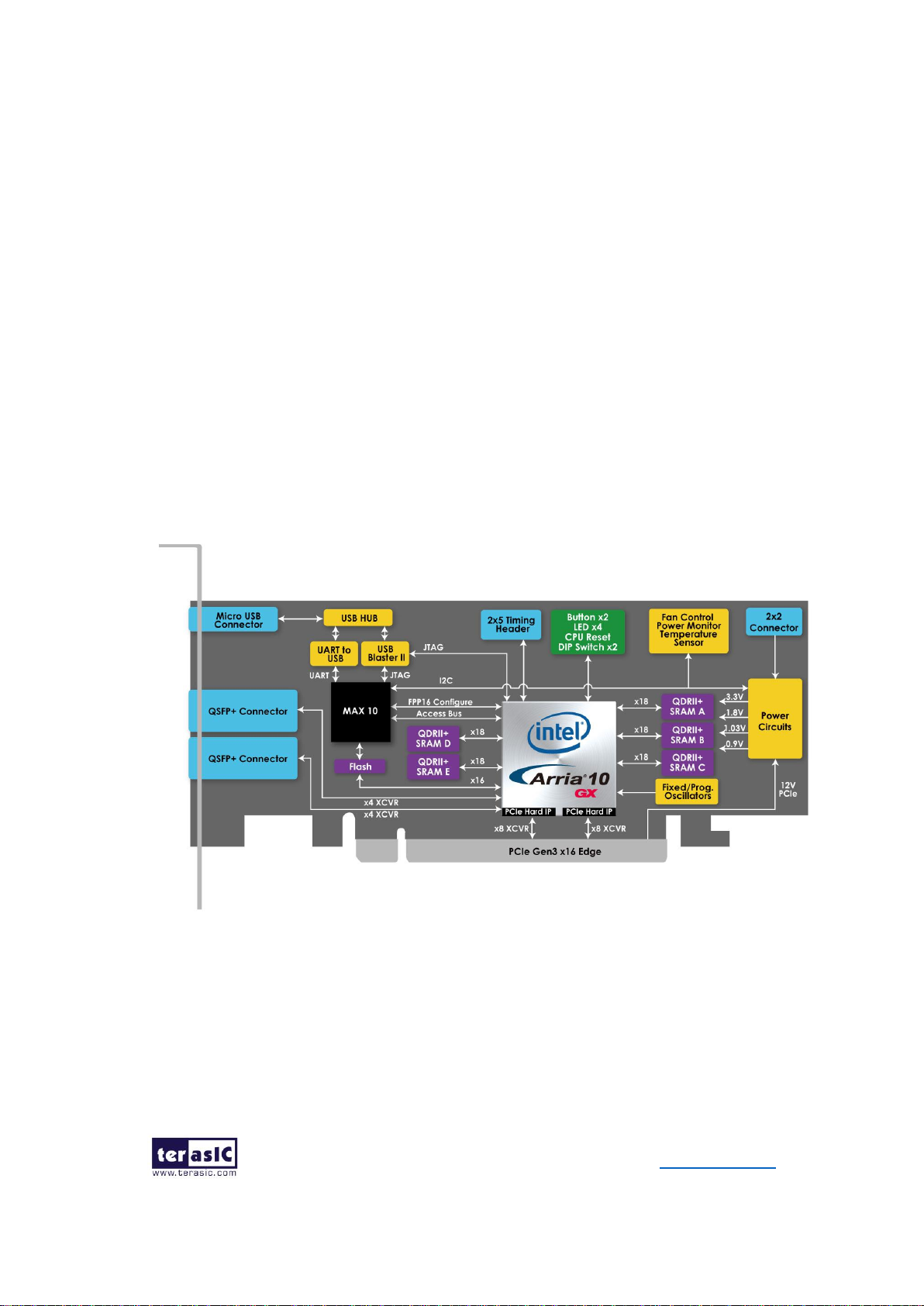
1.3 Block Diagram
Figure 1-1 shows the block diagram of the TR10a-LPQ board. To provide maximum
flexibility for the users, all key components are connected to the Arria 10 GX FPGA
device. Thus, users can configure the FPGA to implement any system design.
Figure 1-1 Block diagram of the TR10a-LPQ board
Below is more detailed information regarding the blocks in Figure 1-1.
◼ Arria 10 GX FPGA
⚫ 10AX115N2F45E1SG
⚫ 1,150K logic elements (LEs)
Page 7

7
TR10a-LPQ User Manual www.terasic.com
December 10,
2018
⚫ 67-Mbits embedded memory
⚫ 48 transceivers (12.5Gbps)
⚫ 3,036 18-bit x 19-bit multipliers
⚫ 1,518 Variable-precision DSP blocks
⚫ 4 PCI Express hard IP blocks
⚫ 768 user I/Os
⚫ 384 LVDS channels
⚫ 32 phase locked loops (PLLs)
◼ FPGA Configuration
⚫ On-board USB Blaster II for use with the Quartus Prime Programmer
⚫ MAX 10 CPLD System Controller and Fast Passive Parallel (FPP x16)
configuration
◼ Memory devices
⚫ 40MB QDRII+ SRAM
⚫ 128MB FLASH
◼ General user I/O
⚫ 4 user controllable LEDs
⚫ 2 user push buttons
⚫ 2 user dip switches
◼ On-Board Clock
⚫ 50MHz oscillator
⚫ Programming PLL providing clock for 40G QSFP+ transceiver
⚫ Programming PLL providing clock for PCIe transceiver
⚫ Programming PLL providing clocks for QDRII+ SRAM
◼ Four QSFP+ ports
⚫ Two QSFP+ connector (40 Gbps+)
◼ Dual PCI Express x8 edge connector
⚫ Support for Dual PCIe x8 Gen1/2/3
⚫ Edge connector for PC motherboard with x16 PCI Express slot
Page 8

8
TR10a-LPQ User Manual www.terasic.com
December 10,
2018
◼ System Monitor and Control
⚫ Temperature sensor
⚫ Fan control
⚫ Power monitor
⚫ UART to USB for board management
◼ Power Source
⚫ PCI Express 4-pin DC 12V power
⚫ PCI Express edge connector power
Page 9
9
TR10a-LPQ User Manual www.terasic.com
December 10,
2018
Chapter 2
Board Components
his chapter introduces all the important components on the TR10a-LPQ.
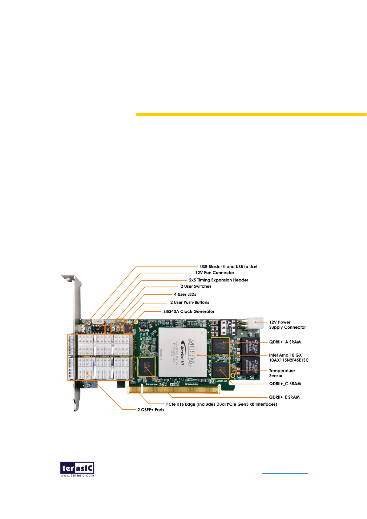
2.1 Board Overview
Figure 2-1 and Figure 2-2 are the top and bottom view of the TR10a-LPQ development
board. It depicts the layout of the board and indicates the location of the connectors and
key components. Users can refer to this figure for relative location of the connectors
and key components.
Figure 2-1 FPGA Board (Top)
T
Page 10

10
TR10a-LPQ User Manual www.terasic.com
December 10,
2018
Figure 2-2 FPGA Board (Bottom)
2.2 Configuration, Status and Setup
◼ Configure
The FPGA board supports two configuration methods for the Arria 10 FPGA:
⚫ Configure the FPGA using the on-board USB-Blaster II.
⚫ Flash memory configuration of the FPGA using stored images from the flash
memory on power-up.
For programming by on-board USB-Blaster II, the following procedures show how to
download a configuration bit stream into the Arria 10 GX FPGA:
⚫ Make sure that power is provided to the FPGA board
⚫ Connect your PC to the FPGA board using a micro-USB cable and make sure
the USB-Blaster II driver is installed on PC.
⚫ Launch Quartus Prime programmer and make sure the USB-Blaster II is
detected.
⚫ In Quartus Prime Programmer, add the configuration bit stream file (.sof),
check the associated “Program/Configure” item, and click “Start” to start
FPGA programming.
Page 11
11
TR10a-LPQ User Manual www.terasic.com
December 10,
2018
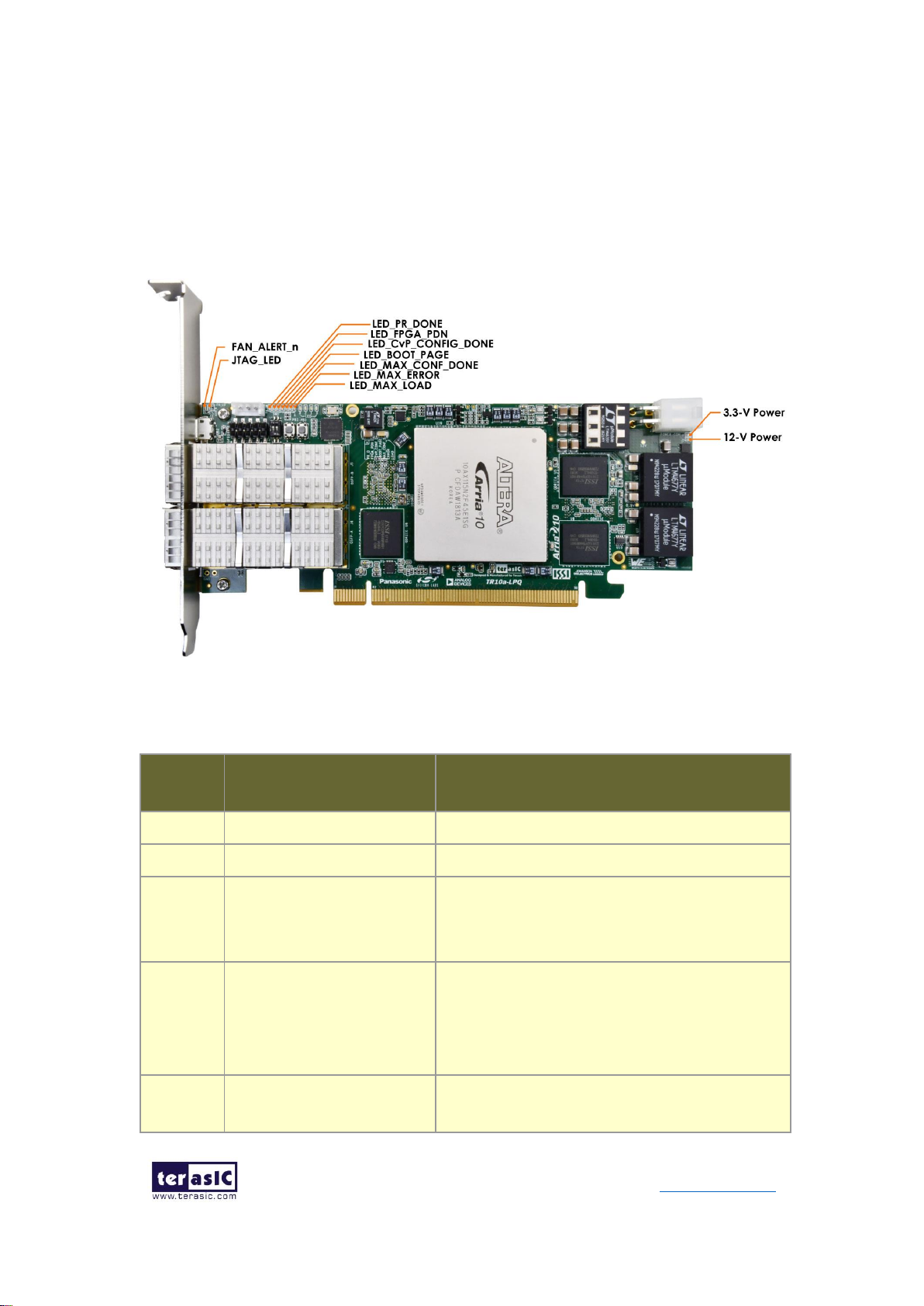
◼ Status LED
The FPGA Board development board includes board-specific status LEDs to indicate
board status as shown in Figure 2-3. Please refer to Table 2-1 for the description of the
LED indicator.
Figure 2-3 Status LED on the TR10a-LPQ
Table 2-1 Status LED
Board
Reference
LED Name
Description
D10
12-V Power
Illuminates when 12-V power is active.
D9
3.3-V Power
Illuminates when 3.3-V power is active.
D6
LED_MAX_CONF_DONE
Illuminates when the FPGA is successfully
configured. Driven by the MAX 10 CPLD
System Controller.
D8
LED_MAX_LOAD
Illuminates when the MAX 10 CPLD System
Controller. is actively configuring the FPGA.
Driven by the MAX 10 CPLD System
Controller. with the Embedded Blaster CPLD.
D7
LED_MAX_ERROR
Illuminates when the MAX 10 CPLD System
Controller. fails to configure the FPGA. Driven
Page 12
12
TR10a-LPQ User Manual www.terasic.com
December 10,
2018
by the MAX 10 CPLD System Controller.
D5
LED_BOOT_PAGE
Illuminates when FPGA is configured by the
factory configuration bit stream.
D3
LED_PR_DONE
Illuminates when FPGA partial reconfiguration
is done
D4
LED_CvP_CONFIG_DONE
Illuminates when FPGA Configuration via
Protocol (CvP) is done
LED6
LED_FPGA_PDN
Illuminates when the temperature of the FPGA
is too high and exceeds the set value, the
FPGA power is automatically turned off.
D1
JTAG_LED
Indicates transmit or receive activity of the
JTAG chain. The LED flickers if the link is in
use and active.
D2
FAN_ALERT_n
Illuminates when the temperature of the FPGA
exceeds the set value.
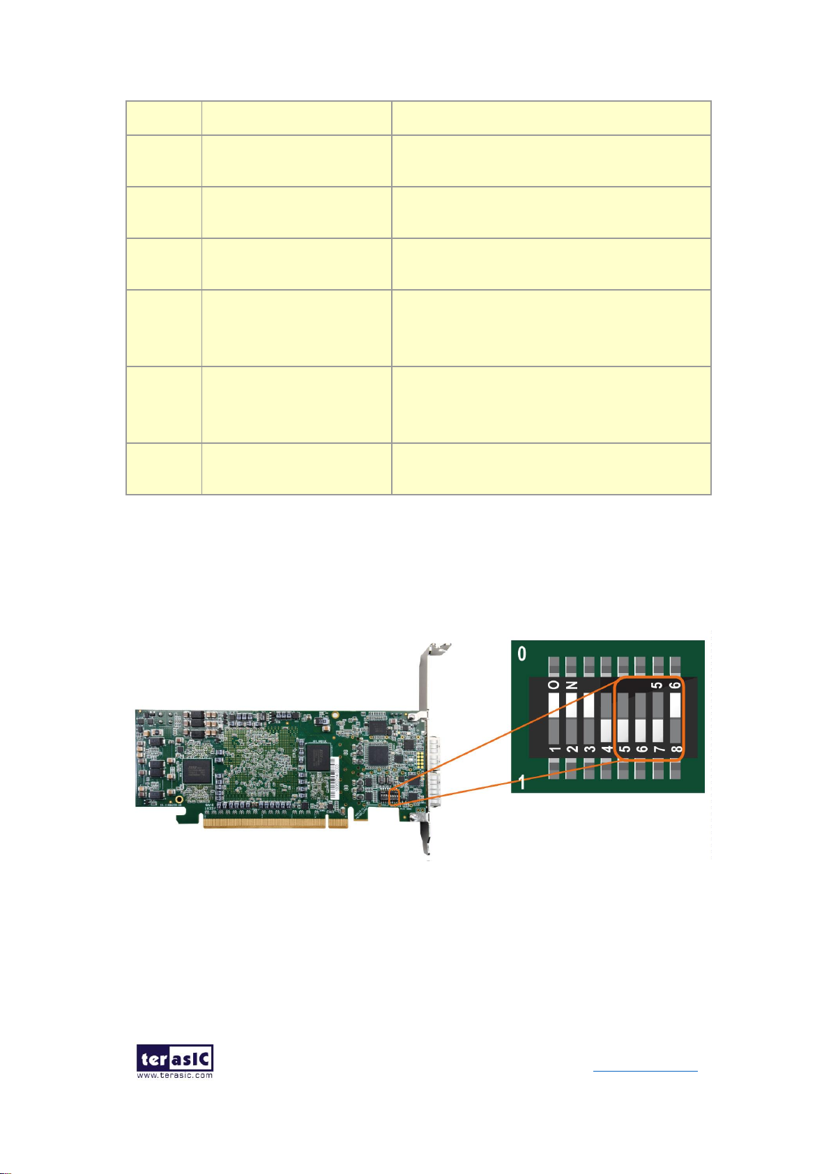
◼ Setup PCI Express Control DIP switch
The PCI Express Control DIP switch (S1) is provided to enable or disable different
configurations of the PCIe Connector. Table 2-2 lists the switch controls and description.
Figure 2-4 Setup PCI Express Control DIP switch
Page 13
13
TR10a-LPQ User Manual www.terasic.com
December 10,
2018
Table 2-2 S1 PCIe Control DIP Switch
Board
Reference
Signal Name
Description
Default
S1.5
PCIE_PRSNT2n_x1
On : Enable x1 presence detect
Off: Disable x1 presence detect
Off
S1.6
PCIE_PRSNT2n_x4
On : Enable x4 presence detect
Off: Disable x4 presence detect
Off
S1.7
PCIE_PRSNT2n_x8
On : Enable x8 presence detect
Off: Disable x8 presence detect
Off
S1.8
PCIE_PRSNT2n_x16
On: Enable dual x8 presence
detect
Off: Disable dual x8 presence
detect
On
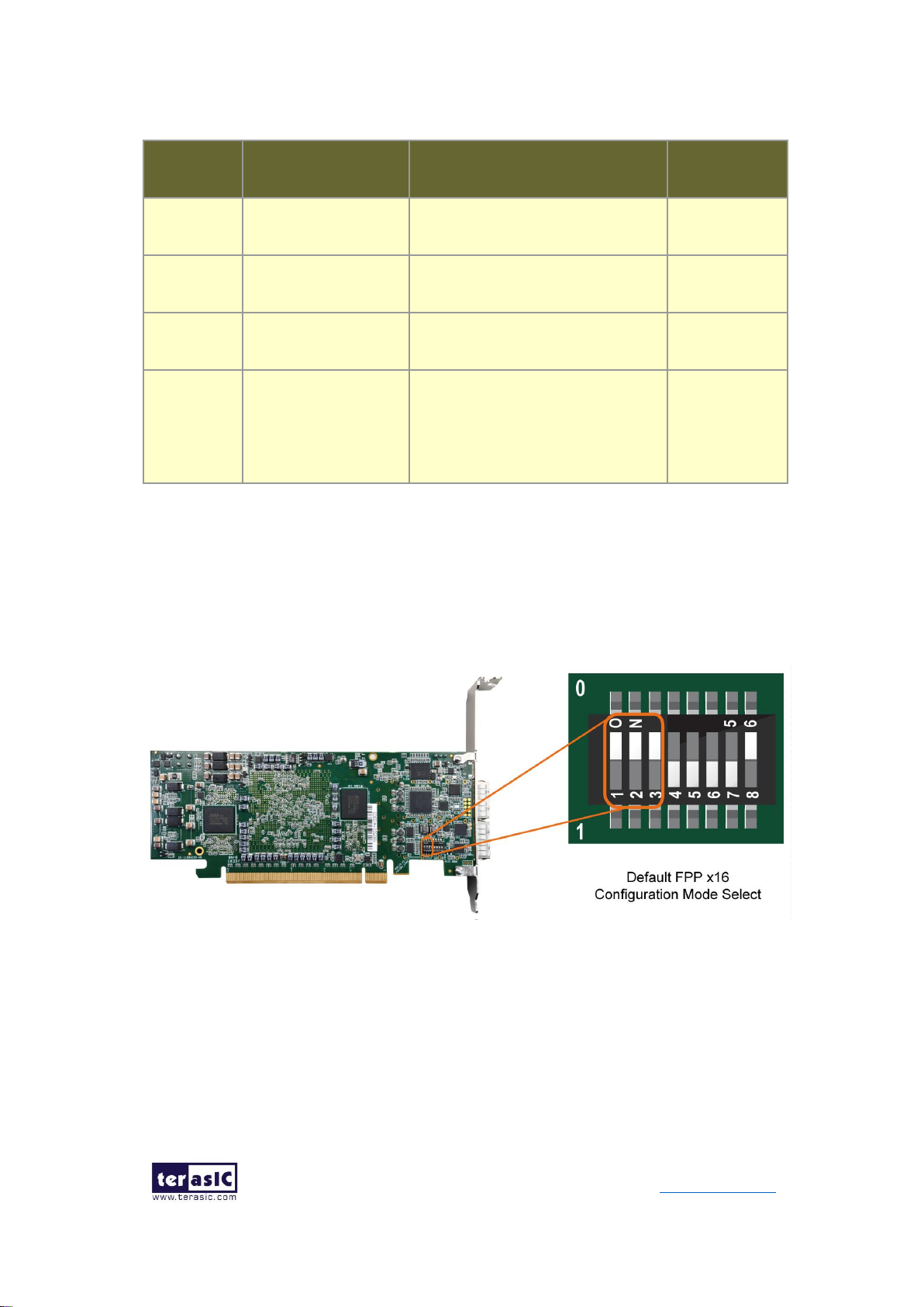
◼ Setup Configure Mode
The position 1~3 of DIP switch S1 are used to specify the configuration mode of the
FPGA. As currently only one mode is supported, please set all positions as shown in
Figure 2-5.
Figure 2-5 Position of DIP switch S1 for Configure Mode
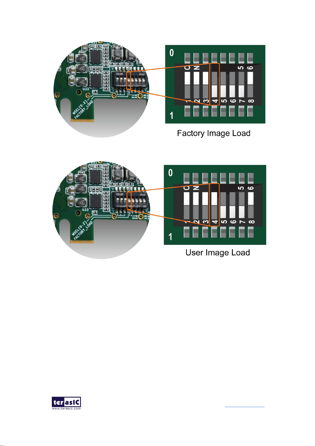
◼ Select Flash Image for Configuration
The position 4 of DIP switch S1 is used to specify the image for configuration of the
FPGA. Setting Position 4 of S1 to “1” (down position) specifies the default factory image
to be loaded, as shown in Figure 2-6. Setting Position 4 of S1 to “0” (up position)
specifies the TR10a-LPQ to load a user-defined image, as shown in Figure 2-7.
Page 14
14
TR10a-LPQ User Manual www.terasic.com
December 10,
2018
Figure 2-6 Position of DIP switch S1 for Image Select – Factory Image Load
Figure 2-7 Position of DIP switch S1 for Image Select – User Image Load
2.3 General User Input/Output
This section describes the user I/O interface to the FPGA.
◼ User Defined Push-buttons
The FPGA board includes four user defined push-buttons that allow users to interact
with the Arria 10 GX device. Each push-button provides a high logic level or a low logic
level when it is not pressed or pressed, respectively. Table 2-3 lists the board references,
signal names and their corresponding Arria 10 GX device pin numbers.
Page 15
15
TR10a-LPQ User Manual www.terasic.com
December 10,
2018
Figure 2-8 User Defined Buttons
Table 2-3 Push-button Pin Assignments, Schematic Signal Names, and
Functions
Board
Reference
Schematic
Signal Name
Description
I/O
Standard
Arria 10 GX
Pin Number
PB0
BUTTON0
High Logic Level when the
button is not pressed
1.8-V
PIN_AR6
PB1
BUTTON1
1.8-V
PIN_AP6
PB4
CPU_RESET_n
1.8-V
AP24
◼ User-Defined Dip Switch
There are two dip switches on the FPGA board to provide additional FPGA input control.
When a dip switch is in the DOWN position or the UPPER position, it provides a high
logic level or a low logic level to the Arria 10 GX FPGA, respectively, as shown in Figure
2-9.
Page 16

16
TR10a-LPQ User Manual www.terasic.com
December 10,
2018
Figure 2-9 2 Dip switches
Table 2-4 lists the signal names and their corresponding Arria 10 GX device pin
numbers.
Table 2-4 Dip Switch Pin Assignments, Schematic Signal Names, and Functions
Board
Reference
Schematic
Signal Name
Description
I/O
Standard
Arria 10 GX
Pin Number
SW0
SW0
High logic level when SW in the
UPPER position.
1.8-V
PIN_ AU35
SW1
1.8-V
PIN_AH33
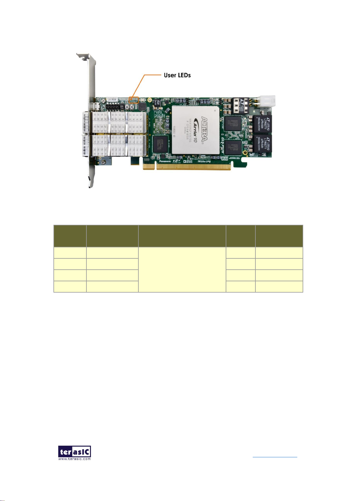
◼ User-Defined LEDs
The FPGA board consists of 4 user-controllable LEDs to allow status and debugging
signals to be driven to the LEDs from the designs loaded into the Arria 10 GX device.
Each LED is driven directly by the Arria 10 GX FPGA. The LED is turned on or off when
the associated pins are driven to a low or high logic level, respectively, as shown in
Figure 2-10. A list of the pin names on the FPGA that are connected to the LEDs is
given in Table 2-5.
Page 17
17
TR10a-LPQ User Manual www.terasic.com
December 10,
2018
Figure 2-10 Four User LEDs
Table 2-5 User LEDs Pin Assignments, Schematic Signal Names, and Functions
Board
Reference
Schematic
Signal Name
Description
I/O
Standard
Arria 10 GX
Pin Number
LED0
LED0
Driving a logic 0 on the I/O port
turns the LED ON.
Driving a logic 1 on the I/O port
turns the LED OFF.
1.8-V
PIN_Y13
LED1
LED1
1.8-V
PIN_Y14
LED2
LED2
1.8-V
PIN_W11
LED3
LED3
1.8-V
PIN_V10
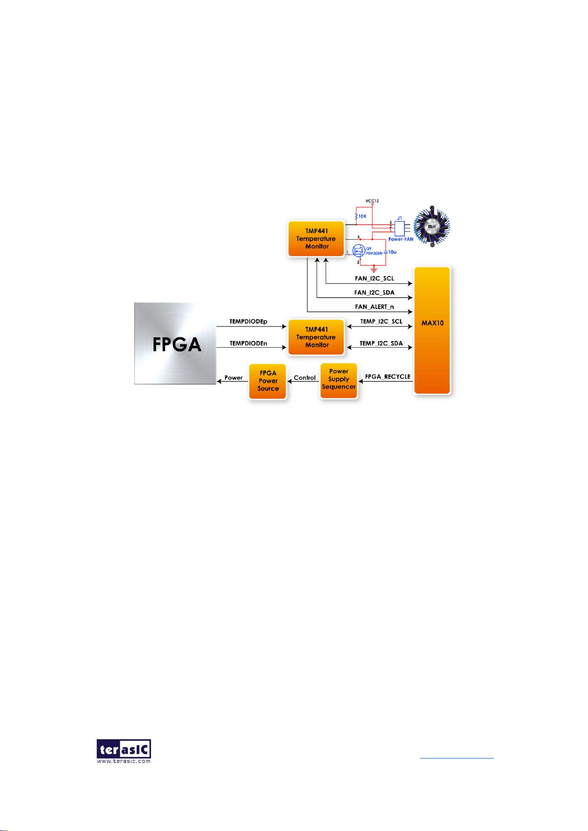
2.4 Temperature Sensor and Fan Control
The TR10a-LPQ has an automatic management system for the temperature of the
FPGA, the fan speed, and the power supply of the FPGA. As shown in Figure 2-11. The
MAX10 FPGA is the main control device on the board.
The temperature of the Arria 10 FPGA is obtained through the TMP441 temperature
sensor and the MAX10 FPGA can read it from TMP441 via I2C bus. The MAX10 FPGA
will adjust the fan speed automatically according to the temperature of the Arria 10
FPGA.
When the board power is on, the fan speed is preset to 3000 rpm. As the temperature
Page 18
18
TR10a-LPQ User Manual www.terasic.com
December 10,
2018
of the Arria10 FPGA rises, the MAX10 will increase the fan speed to decrease the
temperature of the FPGA.
In order to avoid the failure of the fan on the FPGA and stop the rotation and cause the
FPGA temperature to rise rapidly. When the FPGA temperature reaches 95 degrees
(The setting threshold value), the MAX10 will cut off the power supply to the Arria10
FPGA to avoid damage caused by excessive FPGA temperature.
Figure 2-11 The Temperature, Fan Speed and FPGA power control system
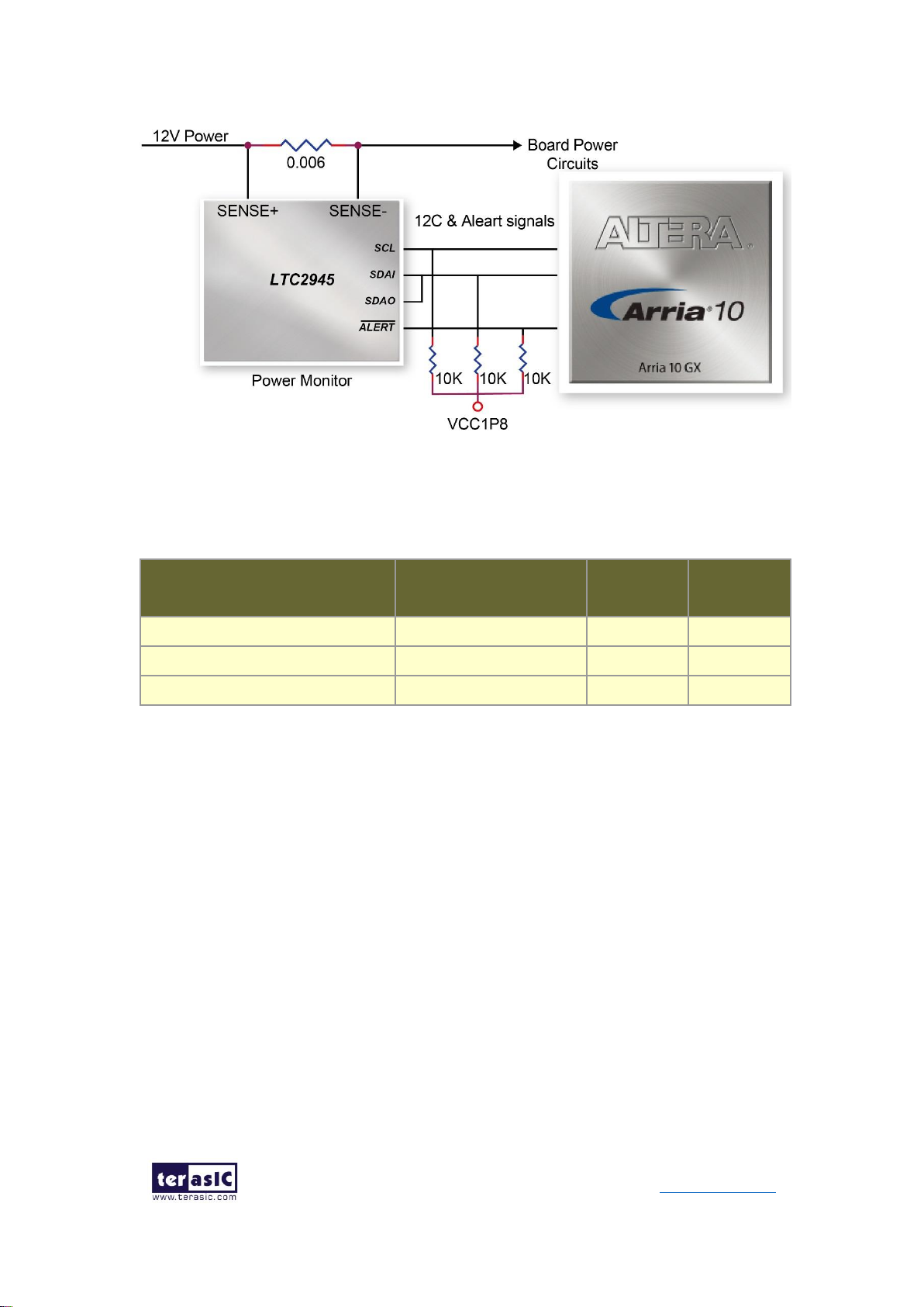
2.5 Power Monitor
The TR10a-LPQ has implemented a power monitor chip to monitor the board input
power voltage and current. Figure 2-12 shows the connection between the power
monitor chip and the Arria 10 GX FPGA. The power monitor chip monitors both shunt
voltage drops and board input power voltage allows user to monitor the total board
power consumption. Programmable calibration value, conversion times, and averaging,
combined with an internal multiplier, enable direct readouts of current in amperes and
power in watts. Table 2-6 shows the pin assignment of power monitor I2C bus.
Page 19
19
TR10a-LPQ User Manual www.terasic.com
December 10,
2018
Figure 2-12 Connections between the Power Monitor chip and the Arria 10 GX
FPGA
Table 2-6 Pin Assignment of Power Monitor I2C bus
Schematic
Signal Name
Description
I/O
Standard
Arria 10 GX
Pin Number
POWER_MONITOR_I2C_SCL
Power Monitor SCL
1.8V
PIN_AT26
POWER_MONITOR_I2C_SDA
Power Monitor SDA
1.8V
PIN_AP25
POWER_MONITOR_ALERT_N
Power Monitor ALERT
1.8V
PIN_BD23
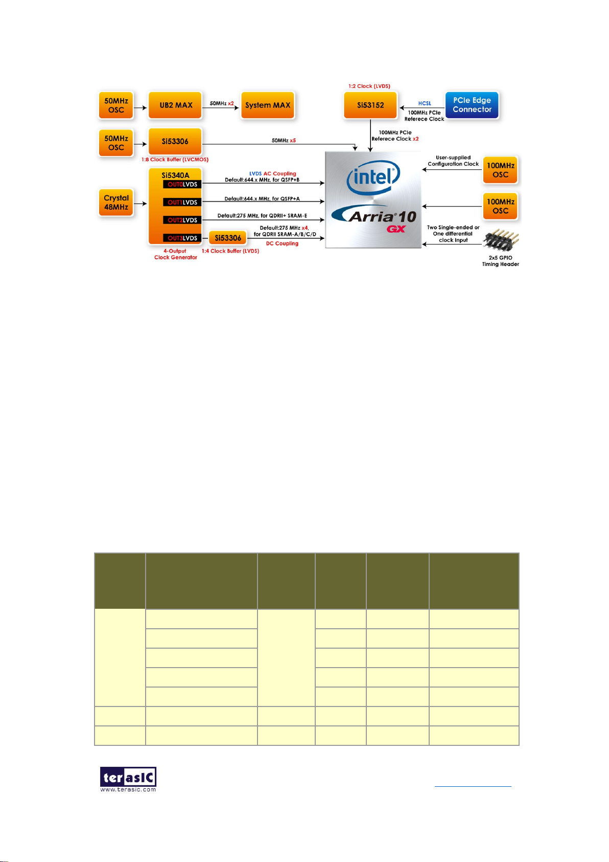
2.6 Clock Circuit
The development board includes four 50 MHz oscillators and two programmable clock
generators. Figure 2-13 shows the default frequencies of on-board all external clocks
going to the Arria 10 GX FPGA.
Page 20
20
TR10a-LPQ User Manual www.terasic.com
December 10,
2018
Figure 2-13 Clock circuit of the FPGA Board
A clock buffer is used to duplicate the 50 MHz oscillator, so there are six 50MHz clocks
fed into different five FPGA banks. The two programming clock generators are low-jitter
oscillators which are used to provide special and high quality clock signals for high-
speed transceivers and high bandwidth memory. Through I2C serial interface, the clock
generator controllers in the Arria 10 GX FPGA can be used to program the Si5340A and
Si5340B to generate 40G Ethernet QSFP+ and high bandwidth memory reference
clocks respectively.
Table 2-7 lists the clock source, signal names, default frequency and their
corresponding Arria 10 GX device pin numbers.
Table 2-7 Clock Source, Signal Name, Default Frequency, Pin Assignments and
Functions
Source
Schematic
Signal Name
Default
Frequency
I/O
Standard
Arria 10 GX
Pin
Number
Application
U38
CLK_50_B2H
50.0 MHz
1.8V
PIN_AP34
User Application
CLK_50_B2I
1.8V
PIN_C30
User Application
CLK_50_B2J
1.8V
PIN_W36
User Application
CLK_50_B3C
1.8V
PIN_AK12
User Application
CLK_50_B3D
1.8V
PIN_AJ11
User Application
Y6
CLK_100_B2J
100.0MHz
1.8V
PIN_AC32
User Application
Y2
OSC_100_CLKUSR
100.0MHz
1.8V
PIN_AV26
User-supplied
Page 21
21
TR10a-LPQ User Manual www.terasic.com
December 10,
2018
configuration
clock
U2
(Si5340A)
QSFPA_REFCLK_p
644.53125
MHz
LVDS
PIN_AH5
40G QSFP+ A
port
QSFPB_REFCLK_p
644.53125
MHz
LVDS
PIN_AD5
40G QSFP+ B
port
QDRIIE_REFCLK_p
275 MHz
LVDS
PIN_AT27
QDRII+ reference
clock for E port
U13
QDRIIA_REFCLK_p
275 MHz
LVDS
PIN_L9
QDRII+ reference
clock for A port
QDRIIB_REFCLK_p
275 MHz
LVDS
PIN_N18
QDRII+ reference
clock for B port
QDRIIC_REFCLK_p
275 MHz
LVDS
PIN_M34
QDRII+ reference
clock for C port
QDRIID_REFCLK_p
275 MHz
LVDS
PIN_BB18
QDRII+ reference
clock for D port
Table 2-8 lists the programmable oscillator control pins, signal names, I/O standard and
their corresponding Arria 10 GX device pin numbers.
Table 2-8 Programmable oscillator control pin, Signal Name, I/O standard, Pin
Assignments and Descriptions
Programmable
Oscillator
Schematic
Signal Name
I/O
Standard
Arria 10 GX
Pin Number
Description
Si5340A
(U2)
Si5340A_I2C_SCL
1.8-V
PIN_F24
I2C bus, connected
with Si5340A
Si5340A_I2C_SDA
1.8-V
PIN_G24
Si5340A_RST
1.8-V
PIN_C27
Si5340A reset
signal
Si5340A_INTR
1.8-V
PIN_C28
Si5340A interrupt
signal
Si5340A_OE_n
1.8-V
PIN_AP39
Si5340A output
enable signal
Page 22
22
TR10a-LPQ User Manual www.terasic.com
December 10,
2018
2.7 FLASH Memory
The development board has one 1Gb CFI-compatible synchronous flash device for non-
volatile storage of FPGA configuration data, user application data, and user code space.
Each interface has a 16-bit data bus and the device combined allow for FPP x16
configuration. This device is part of the shared flash and MAX (FM) bus, which connects
to the flash memory and MAX V CPLD System Controller. Figure 2-14 shows the
connections between the Flash, MAX and Arria 10 GX FPGA.
Figure 2-14 Connection between the Flash, Max and Arria 10 GX FPGA
Table 2-9 lists the flash pin assignments, signal names, and functions.
Table 2-9 Flash Memory Pin Assignments, Schematic Signal Names, and
Functions
Schematic
Signal Name
Description
I/O Standard
Arria 10 GX Pin
Number
FLASH_A1
Address bus
1.8-V
PIN_AE14
FLASH_A2
Address bus
1.8-V
PIN_AT7
FLASH_A3
Address bus
1.8-V
PIN_AC11
FLASH_A4
Address bus
1.8-V
PIN_AC13
FLASH_A5
Address bus
1.8-V
PIN_AC12
FLASH_A6
Address bus
1.8-V
PIN_AF14
FLASH_A7
Address bus
1.8-V
PIN_AD13
Page 23

23
TR10a-LPQ User Manual www.terasic.com
December 10,
2018
FLASH_A8
Address bus
1.8-V
PIN_AG14
FLASH_A9
Address bus
1.8-V
PIN_AJ13
FLASH_A10
Address bus
1.8-V
PIN_AE13
FLASH_A11
Address bus
1.8-V
PIN_AB14
FLASH_A12
Address bus
1.8-V
PIN_AH12
FLASH_A13
Address bus
1.8-V
PIN_AK13
FLASH_A14
Address bus
1.8-V
PIN_AL12
FLASH_A15
Address bus
1.8-V
PIN_AV7
FLASH_A16
Address bus
1.8-V
PIN_AJ10
FLASH_A17
Address bus
1.8-V
PIN_AH13
FLASH_A18
Address bus
1.8-V
PIN_AN12
FLASH_A19
Address bus
1.8-V
PIN_AU9
FLASH_A20
Address bus
1.8-V
PIN_AV6
FLASH_A21
Address bus
1.8-V
PIN_AT6
FLASH_A22
Address bus
1.8-V
PIN_AR9
FLASH_A23
Address bus
1.8-V
PIN_AB13
FLASH_A24
Address bus
1.8-V
PIN_AF12
FLASH_A25
Address bus
1.8-V
PIN_AT9
FLASH_A26
Address bus
1.8-V
PIN_AV8
FLASH_A27
Address bus (Reserve)
1.8-V
PIN_AB12
FLASH_D0
Data bus
1.8-V
PIN_AN11
FLASH_D1
Data bus
1.8-V
PIN_AT12
FLASH_D2
Data bus
1.8-V
PIN_AP8
FLASH_D3
Data bus
1.8-V
PIN_AT11
FLASH_D4
Data bus
1.8-V
PIN_AR11
FLASH_D5
Data bus
1.8-V
PIN_AR7
FLASH_D6
Data bus
1.8-V
PIN_AU8
FLASH_D7
Data bus
1.8-V
PIN_AR8
FLASH_D8
Data bus
1.8-V
PIN_AN10
FLASH_D9
Data bus
1.8-V
PIN_AR12
FLASH_D10
Data bus
1.8-V
PIN_AP10
FLASH_D11
Data bus
1.8-V
PIN_AP11
FLASH_D12
Data bus
1.8-V
PIN_AT10
FLASH_D13
Data bus
1.8-V
PIN_AP9
FLASH_D14
Data bus
1.8-V
PIN_AU7
Page 24
24
TR10a-LPQ User Manual www.terasic.com
December 10,
2018
FLASH_D15
Data bus
1.8-V
PIN_AU10
FLASH_CLK
Clock
1.8-V
PIN_AM12
FLASH_RESET_n
Reset
1.8-V
PIN_AE12
FLASH_CE_n
Chip enable of flash
1.8-V
PIN_AL11
FLASH_OE_n
Output enable
1.8-V
PIN_AH10
FLASH_WE_n
Write enable
1.8-V
PIN_AG12
FLASH_ADV_n
Address valid
1.8-V
PIN_AD14
FLASH_RDY_BS
Y_n
Ready of flash
1.8-V
PIN_AG13
2.8 QDRII+ SRAM
The development board supports five independent QDRII+ SRAM memory devices for
very-high speed and low-latency memory access. Each of QDRII+ has a x18 interface,
providing addressing to a device of up to a 8MB (not including parity bits). The QDRII+
has separate read and write data ports with DDR signaling at up to 550 MHz.
Table 2-10, Table 2-11, Table 2-12, Table 2-13 and
Table 2-14 lists the QDRII+ SRAM Bank A, B, C, D and E pin assignments, signal
names relative to the Arria 10 GX device, in respectively.
Table 2-10 QDRII+ SRAM A Pin Assignments, Schematic Signal Names, and
Functions
Schematic
Signal Name
Description
I/O Standard
Arria 10 GX Pin
Number
QDRIIA_A0
Address bus[0]
1.8-V HSTL Class I
PIN_V12
QDRIIA_A1
Address bus[1]
1.8-V HSTL Class I
PIN_V13
QDRIIA_A2
Address bus[2]
1.8-V HSTL Class I
PIN_N10
QDRIIA_A3
Address bus[3]
1.8-V HSTL Class I
PIN_M10
QDRIIA_A4
Address bus[4]
1.8-V HSTL Class I
PIN_P11
QDRIIA_A5
Address bus[5]
1.8-V HSTL Class I
PIN_N11
QDRIIA_A6
Address bus[6]
1.8-V HSTL Class I
PIN_M9
QDRIIA_A7
Address bus[7]
1.8-V HSTL Class I
PIN_M8
QDRIIA_A8
Address bus[8]
1.8-V HSTL Class I
PIN_N7
Page 25

25
TR10a-LPQ User Manual www.terasic.com
December 10,
2018
QDRIIA_A9
Address bus[9]
1.8-V HSTL Class I
PIN_N8
QDRIIA_A10
Address bus[10]
1.8-V HSTL Class I
PIN_P10
QDRIIA_A11
Address bus[11]
1.8-V HSTL Class I
PIN_P9
QDRIIA_A12
Address bus[12]
1.8-V HSTL Class I
PIN_N6
QDRIIA_A13
Address bus[13]
1.8-V HSTL Class I
PIN_M7
QDRIIA_A14
Address bus[14]
1.8-V HSTL Class I
PIN_L10
QDRIIA_A15
Address bus[15]
1.8-V HSTL Class I
PIN_L7
QDRIIA_A16
Address bus[16]
1.8-V HSTL Class I
PIN_K7
QDRIIA_A17
Address bus[17]
1.8-V HSTL Class I
PIN_K8
QDRIIA_A18
Address bus[18]
1.8-V HSTL Class I
PIN_J9
QDRIIA_A19
Address bus[19]
1.8-V HSTL Class I
PIN_L6
QDRIIA_A20
Address bus[20]
1.8-V HSTL Class I
PIN_K6
QDRIIA_A21
Address bus[21]
1.8-V HSTL Class I
PIN_J6
QDRIIA_D0
Write data bus[0]
1.8-V HSTL Class I
PIN_C13
QDRIIA_D1
Write data bus[1]
1.8-V HSTL Class I
PIN_D13
QDRIIA_D2
Write data bus[2]
1.8-V HSTL Class I
PIN_E13
QDRIIA_D3
Write data bus[3]
1.8-V HSTL Class I
PIN_B13
QDRIIA_D4
Write data bus[4]
1.8-V HSTL Class I
PIN_E11
QDRIIA_D5
Write data bus[5]
1.8-V HSTL Class I
PIN_C12
QDRIIA_D6
Write data bus[6]
1.8-V HSTL Class I
PIN_B12
QDRIIA_D7
Write data bus[7]
1.8-V HSTL Class I
PIN_A12
QDRIIA_D8
Write data bus[8]
1.8-V HSTL Class I
PIN_D11
QDRIIA_D9
Write data bus[9]
1.8-V HSTL Class I
PIN_E9
QDRIIA_D10
Write data bus[10]
1.8-V HSTL Class I
PIN_C8
QDRIIA_D11
Write data bus[11]
1.8-V HSTL Class I
PIN_D8
QDRIIA_D12
Write data bus[12]
1.8-V HSTL Class I
PIN_D9
QDRIIA_D13
Write data bus[13]
1.8-V HSTL Class I
PIN_D10
QDRIIA_D14
Write data bus[14]
1.8-V HSTL Class I
PIN_B10
QDRIIA_D15
Write data bus[15]
1.8-V HSTL Class I
PIN_A10
QDRIIA_D16
Write data bus[16]
1.8-V HSTL Class I
PIN_A11
QDRIIA_D17
Write data bus[17]
1.8-V HSTL Class I
PIN_C11
QDRIIA_Q0
Read Data bus[0]
1.8-V HSTL Class I
PIN_H12
QDRIIA_Q1
Read Data bus[1]
1.8-V HSTL Class I
PIN_K12
QDRIIA_Q2
Read Data bus[2]
1.8-V HSTL Class I
PIN_J14
QDRIIA_Q3
Read Data bus[3]
1.8-V HSTL Class I
PIN_H11
Page 26
26
TR10a-LPQ User Manual www.terasic.com
December 10,
2018
QDRIIA_Q4
Read Data bus[4]
1.8-V HSTL Class I
PIN_K13
QDRIIA_Q5
Read Data bus[5]
1.8-V HSTL Class I
PIN_G10
QDRIIA_Q6
Read Data bus[6]
1.8-V HSTL Class I
PIN_L12
QDRIIA_Q7
Read Data bus[7]
1.8-V HSTL Class I
PIN_P13
QDRIIA_Q8
Read Data bus[8]
1.8-V HSTL Class I
PIN_M13
QDRIIA_Q9
Read Data bus[9]
1.8-V HSTL Class I
PIN_T14
QDRIIA_Q10
Read Data bus[10]
1.8-V HSTL Class I
PIN_R13
QDRIIA_Q11
Read Data bus[11]
1.8-V HSTL Class I
PIN_R12
QDRIIA_Q12
Read Data bus[12]
1.8-V HSTL Class I
PIN_R14
QDRIIA_Q13
Read Data bus[13]
1.8-V HSTL Class I
PIN_N13
QDRIIA_Q14
Read Data bus[14]
1.8-V HSTL Class I
PIN_M14
QDRIIA_Q15
Read Data bus[15]
1.8-V HSTL Class I
PIN_N12
QDRIIA_Q16
Read Data bus[16]
1.8-V HSTL Class I
PIN_L14
QDRIIA_Q17
Read Data bus[17]
1.8-V HSTL Class I
PIN_M12
QDRIIA_BWS_n0
Byte Write select[0]
1.8-V HSTL Class I
PIN_C10
QDRIIA_BWS_n1
Byte Write select[1]
1.8-V HSTL Class I
PIN_E8
QDRIIA_K_P
Clock P
Differential 1.8-V HSTL
Class I
PIN_F12
QDRIIA_K_N
Clock N
Differential 1.8-V HSTL
Class I
PIN_E12
QDRIIA_CQ_P
Echo clock P
1.8-V HSTL Class I
PIN_J13
QDRIIA_CQ_N
Echo clock N
1.8-V HSTL Class I
PIN_H13
QDRIIA_RPS_n
Report Select
1.8-V HSTL Class I
PIN_U9
QDRIIA_WPS_n
Write Port Select
1.8-V HSTL Class I
PIN_U8
QDRIIA_DOFF_n
DLL enable
1.8-V HSTL Class I
PIN_R9
QDRIIA_ODT
On-Die Termination
Input
1.8-V HSTL Class I
PIN_T10
QDRIIA_QVLD
Valid Output
1.8-V HSTL Class I
PIN_K14
Table 2-11 QDRII+ SRAM B Pin Assignments, Schematic Signal Names, and
Functions
Schematic
Signal Name
Description
I/O Standard
Arria 10 GX Pin
Number
QDRIIB_A0
Address bus[0]
1.8-V HSTL Class I
PIN_L16
QDRIIB_A1
Address bus[1]
1.8-V HSTL Class I
PIN_L15
Page 27

27
TR10a-LPQ User Manual www.terasic.com
December 10,
2018
QDRIIB_A2
Address bus[2]
1.8-V HSTL Class I
PIN_E14
QDRIIB_A3
Address bus[3]
1.8-V HSTL Class I
PIN_D14
QDRIIB_A4
Address bus[4]
1.8-V HSTL Class I
PIN_G14
QDRIIB_A5
Address bus[5]
1.8-V HSTL Class I
PIN_F14
QDRIIB_A6
Address bus[6]
1.8-V HSTL Class I
PIN_D15
QDRIIB_A7
Address bus[7]
1.8-V HSTL Class I
PIN_C15
QDRIIB_A8
Address bus[8]
1.8-V HSTL Class I
PIN_F15
QDRIIB_A9
Address bus[9]
1.8-V HSTL Class I
PIN_F16
QDRIIB_A10
Address bus[10]
1.8-V HSTL Class I
PIN_H15
QDRIIB_A11
Address bus[11]
1.8-V HSTL Class I
PIN_G15
QDRIIB_A12
Address bus[12]
1.8-V HSTL Class I
PIN_E16
QDRIIB_A13
Address bus[13]
1.8-V HSTL Class I
PIN_D16
QDRIIB_A14
Address bus[14]
1.8-V HSTL Class I
PIN_E17
QDRIIB_A15
Address bus[15]
1.8-V HSTL Class I
PIN_G17
QDRIIB_A16
Address bus[16]
1.8-V HSTL Class I
PIN_G18
QDRIIB_A17
Address bus[17]
1.8-V HSTL Class I
PIN_L17
QDRIIB_A18
Address bus[18]
1.8-V HSTL Class I
PIN_K17
QDRIIB_A19
Address bus[19]
1.8-V HSTL Class I
PIN_H17
QDRIIB_A20
Address bus[20]
1.8-V HSTL Class I
PIN_H18
QDRIIB_A21
Address bus[21]
1.8-V HSTL Class I
PIN_K18
QDRIIB_D0
Write data bus[0]
1.8-V HSTL Class I
PIN_C18
QDRIIB_D1
Write data bus[1]
1.8-V HSTL Class I
PIN_G19
QDRIIB_D2
Write data bus[2]
1.8-V HSTL Class I
PIN_J19
QDRIIB_D3
Write data bus[3]
1.8-V HSTL Class I
PIN_D19
QDRIIB_D4
Write data bus[4]
1.8-V HSTL Class I
PIN_K19
QDRIIB_D5
Write data bus[5]
1.8-V HSTL Class I
PIN_L19
QDRIIB_D6
Write data bus[6]
1.8-V HSTL Class I
PIN_B20
QDRIIB_D7
Write data bus[7]
1.8-V HSTL Class I
PIN_M19
QDRIIB_D8
Write data bus[8]
1.8-V HSTL Class I
PIN_B19
QDRIIB_D9
Write data bus[9]
1.8-V HSTL Class I
PIN_N20
QDRIIB_D10
Write data bus[10]
1.8-V HSTL Class I
PIN_M20
QDRIIB_D11
Write data bus[11]
1.8-V HSTL Class I
PIN_L21
QDRIIB_D12
Write data bus[12]
1.8-V HSTL Class I
PIN_L20
QDRIIB_D13
Write data bus[13]
1.8-V HSTL Class I
PIN_F20
QDRIIB_D14
Write data bus[14]
1.8-V HSTL Class I
PIN_F19
Page 28

28
TR10a-LPQ User Manual www.terasic.com
December 10,
2018
QDRIIB_D15
Write data bus[15]
1.8-V HSTL Class I
PIN_H20
QDRIIB_D16
Write data bus[16]
1.8-V HSTL Class I
PIN_J20
QDRIIB_D17
Write data bus[17]
1.8-V HSTL Class I
PIN_G20
QDRIIB_Q0
Read Data bus[0]
1.8-V HSTL Class I
PIN_G23
QDRIIB_Q1
Read Data bus[1]
1.8-V HSTL Class I
PIN_F21
QDRIIB_Q2
Read Data bus[2]
1.8-V HSTL Class I
PIN_G22
QDRIIB_Q3
Read Data bus[3]
1.8-V HSTL Class I
PIN_H23
QDRIIB_Q4
Read Data bus[4]
1.8-V HSTL Class I
PIN_H21
QDRIIB_Q5
Read Data bus[5]
1.8-V HSTL Class I
PIN_H22
QDRIIB_Q6
Read Data bus[6]
1.8-V HSTL Class I
PIN_J23
QDRIIB_Q7
Read Data bus[7]
1.8-V HSTL Class I
PIN_K22
QDRIIB_Q8
Read Data bus[8]
1.8-V HSTL Class I
PIN_L22
QDRIIB_Q9
Read Data bus[9]
1.8-V HSTL Class I
PIN_B23
QDRIIB_Q10
Read Data bus[10]
1.8-V HSTL Class I
PIN_A21
QDRIIB_Q11
Read Data bus[11]
1.8-V HSTL Class I
PIN_F22
QDRIIB_Q12
Read Data bus[12]
1.8-V HSTL Class I
PIN_E22
QDRIIB_Q13
Read Data bus[13]
1.8-V HSTL Class I
PIN_C21
QDRIIB_Q14
Read Data bus[14]
1.8-V HSTL Class I
PIN_A22
QDRIIB_Q15
Read Data bus[15]
1.8-V HSTL Class I
PIN_E23
QDRIIB_Q16
Read Data bus[16]
1.8-V HSTL Class I
PIN_B22
QDRIIB_Q17
Read Data bus[17]
1.8-V HSTL Class I
PIN_C22
QDRIIB_BWS_n0
Byte Write select[0]
1.8-V HSTL Class I
PIN_C20
QDRIIB_BWS_n1
Byte Write select[1]
1.8-V HSTL Class I
PIN_E19
QDRIIB_K_p
Clock P
Differential 1.8-V HSTL
Class I
PIN_K21
QDRIIB_K_n
Clock N
Differential 1.8-V HSTL
Class I
PIN_J21
QDRIIB_CQ_p
Echo clock P
1.8-V HSTL Class I
PIN_D23
QDRIIB_CQ_n
Echo clock N
1.8-V HSTL Class I
PIN_C23
QDRIIB_RPS_n
Report Select
1.8-V HSTL Class I
PIN_J16
QDRIIB_WPS_n
Write Port Select
1.8-V HSTL Class I
PIN_K16
QDRIIB_DOFF_n
PLL Turn Off
1.8-V HSTL Class I
PIN_H16
QDRIIB_ODT
On-Die Termination
Input
1.8-V HSTL Class I
PIN_M17
QDRIIB_QVLD
Valid Output
1.8-V HSTL Class I
PIN_K23
Page 29
29
TR10a-LPQ User Manual www.terasic.com
December 10,
2018
Indicator
Table 2-12 QDRII+ SRAM C Pin Assignments, Schematic Signal Names, and
Functions
Schematic
Signal Name
Description
I/O Standard
Arria 10 GX Pin
Number
QDRIIC_A0
Address bus[0]
1.8-V HSTL Class I
PIN_Y32
QDRIIC_A1
Address bus[1]
1.8-V HSTL Class I
PIN_W33
QDRIIC_A2
Address bus[2]
1.8-V HSTL Class I
PIN_P34
QDRIIC_A3
Address bus[3]
1.8-V HSTL Class I
PIN_P33
QDRIIC_A4
Address bus[4]
1.8-V HSTL Class I
PIN_L32
QDRIIC_A5
Address bus[5]
1.8-V HSTL Class I
PIN_K32
QDRIIC_A6
Address bus[6]
1.8-V HSTL Class I
PIN_R34
QDRIIC_A7
Address bus[7]
1.8-V HSTL Class I
PIN_R33
QDRIIC_A8
Address bus[8]
1.8-V HSTL Class I
PIN_T32
QDRIIC_A9
Address bus[9]
1.8-V HSTL Class I
PIN_R32
QDRIIC_A10
Address bus[10]
1.8-V HSTL Class I
PIN_N32
QDRIIC_A11
Address bus[11]
1.8-V HSTL Class I
PIN_M32
QDRIIC_A12
Address bus[12]
1.8-V HSTL Class I
PIN_T31
QDRIIC_A13
Address bus[13]
1.8-V HSTL Class I
PIN_R31
QDRIIC_A14
Address bus[14]
1.8-V HSTL Class I
PIN_K38
QDRIIC_A15
Address bus[15]
1.8-V HSTL Class I
PIN_L37
QDRIIC_A16
Address bus[16]
1.8-V HSTL Class I
PIN_K36
QDRIIC_A17
Address bus[17]
1.8-V HSTL Class I
PIN_N33
QDRIIC_A18
Address bus[18]
1.8-V HSTL Class I
PIN_M33
QDRIIC_A19
Address bus[19]
1.8-V HSTL Class I
PIN_L39
QDRIIC_A20
Address bus[20]
1.8-V HSTL Class I
PIN_K39
QDRIIC_A21
Address bus[21]
1.8-V HSTL Class I
PIN_L35
QDRIIC_D0
Write data bus[0]
1.8-V HSTL Class I
PIN_E34
QDRIIC_D1
Write data bus[1]
1.8-V HSTL Class I
PIN_D36
QDRIIC_D2
Write data bus[2]
1.8-V HSTL Class I
PIN_E36
QDRIIC_D3
Write data bus[3]
1.8-V HSTL Class I
PIN_D35
QDRIIC_D4
Write data bus[4]
1.8-V HSTL Class I
PIN_E37
QDRIIC_D5
Write data bus[5]
1.8-V HSTL Class I
PIN_F39
QDRIIC_D6
Write data bus[6]
1.8-V HSTL Class I
PIN_F37
Page 30

30
TR10a-LPQ User Manual www.terasic.com
December 10,
2018
QDRIIC_D7
Write data bus[7]
1.8-V HSTL Class I
PIN_G39
QDRIIC_D8
Write data bus[8]
1.8-V HSTL Class I
PIN_F36
QDRIIC_D9
Write data bus[9]
1.8-V HSTL Class I
PIN_G30
QDRIIC_D10
Write data bus[10]
1.8-V HSTL Class I
PIN_D33
QDRIIC_D11
Write data bus[11]
1.8-V HSTL Class I
PIN_H30
QDRIIC_D12
Write data bus[12]
1.8-V HSTL Class I
PIN_D34
QDRIIC_D13
Write data bus[13]
1.8-V HSTL Class I
PIN_G29
QDRIIC_D14
Write data bus[14]
1.8-V HSTL Class I
PIN_E33
QDRIIC_D15
Write data bus[15]
1.8-V HSTL Class I
PIN_E31
QDRIIC_D16
Write data bus[16]
1.8-V HSTL Class I
PIN_F31
QDRIIC_D17
Write data bus[17]
1.8-V HSTL Class I
PIN_F30
QDRIIC_Q0
Read Data bus[0]
1.8-V HSTL Class I
PIN_P31
QDRIIC_Q1
Read Data bus[1]
1.8-V HSTL Class I
PIN_N31
QDRIIC_Q2
Read Data bus[2]
1.8-V HSTL Class I
PIN_G33
QDRIIC_Q3
Read Data bus[3]
1.8-V HSTL Class I
PIN_G32
QDRIIC_Q4
Read Data bus[4]
1.8-V HSTL Class I
PIN_J31
QDRIIC_Q5
Read Data bus[5]
1.8-V HSTL Class I
PIN_G34
QDRIIC_Q6
Read Data bus[6]
1.8-V HSTL Class I
PIN_L31
QDRIIC_Q7
Read Data bus[7]
1.8-V HSTL Class I
PIN_L30
QDRIIC_Q8
Read Data bus[8]
1.8-V HSTL Class I
PIN_J30
QDRIIC_Q9
Read Data bus[9]
1.8-V HSTL Class I
PIN_P28
QDRIIC_Q10
Read Data bus[10]
1.8-V HSTL Class I
PIN_N28
QDRIIC_Q11
Read Data bus[11]
1.8-V HSTL Class I
PIN_M28
QDRIIC_Q12
Read Data bus[12]
1.8-V HSTL Class I
PIN_M29
QDRIIC_Q13
Read Data bus[13]
1.8-V HSTL Class I
PIN_N30
QDRIIC_Q14
Read Data bus[14]
1.8-V HSTL Class I
PIN_M30
QDRIIC_Q15
Read Data bus[15]
1.8-V HSTL Class I
PIN_L29
QDRIIC_Q16
Read Data bus[16]
1.8-V HSTL Class I
PIN_K29
QDRIIC_Q17
Read Data bus[17]
1.8-V HSTL Class I
PIN_J29
QDRIIC_BWS_n0
Byte Write select[0]
1.8-V HSTL Class I
PIN_F34
QDRIIC_BWS_n1
Byte Write select[1]
1.8-V HSTL Class I
PIN_C37
QDRIIC_K_p
Clock P
Differential 1.8-V
HSTL Class I
PIN_F32
QDRIIC_K_n
Clock N
Differential 1.8-V
HSTL Class I
PIN_E32
Page 31

31
TR10a-LPQ User Manual www.terasic.com
December 10,
2018
QDRIIC_CQ_p
Echo clock P
1.8-V HSTL Class I
PIN_G35
QDRIIC_CQ_n
Echo clock N
1.8-V HSTL Class I
PIN_F35
QDRIIC_RPS_n
Report Select
1.8-V HSTL Class I
PIN_E26
QDRIIC_WPS_n
Write Port Select
1.8-V HSTL Class I
PIN_V33
QDRIIC_DOFF_n
PLL Turn Off
1.8-V HSTL Class I
PIN_ W31
QDRIIC_ODT
On-Die Termination
Input
1.8-V HSTL Class I
PIN_Y33
QDRIIC_QVLD
Valid Output Indicator
1.8-V HSTL Class I
PIN_K31
Table 2-13 QDRII+ SRAM D Pin Assignments, Schematic Signal Names, and
Functions
Schematic
Signal Name
Description
I/O Standard
Arria 10 GX
Pin Number
QDRIID_A0
Address bus[0]
1.8-V HSTL Class I
PIN_AT17
QDRIID_A1
Address bus[1]
1.8-V HSTL Class I
PIN_AU17
QDRIID_A2
Address bus[2]
1.8-V HSTL Class I
PIN_AV16
QDRIID_A3
Address bus[3]
1.8-V HSTL Class I
PIN_AV17
QDRIID_A4
Address bus[4]
1.8-V HSTL Class I
PIN_AU15
QDRIID_A5
Address bus[5]
1.8-V HSTL Class I
PIN_AV15
QDRIID_A6
Address bus[6]
1.8-V HSTL Class I
PIN_BA15
QDRIID_A7
Address bus[7]
1.8-V HSTL Class I
PIN_BA16
QDRIID_A8
Address bus[8]
1.8-V HSTL Class I
PIN_AY17
QDRIID_A9
Address bus[9]
1.8-V HSTL Class I
PIN_BA17
QDRIID_A10
Address bus[10]
1.8-V HSTL Class I
PIN_AW16
QDRIID_A11
Address bus[11]
1.8-V HSTL Class I
PIN_AY16
QDRIID_A12
Address bus[12]
1.8-V HSTL Class I
PIN_AW18
QDRIID_A13
Address bus[13]
1.8-V HSTL Class I
PIN_AY18
QDRIID_A14
Address bus[14]
1.8-V HSTL Class I
PIN_BC15
QDRIID_A15
Address bus[15]
1.8-V HSTL Class I
PIN_BD13
QDRIID_A16
Address bus[16]
1.8-V HSTL Class I
PIN_BD14
QDRIID_A17
Address bus[17]
1.8-V HSTL Class I
PIN_BC18
QDRIID_A18
Address bus[18]
1.8-V HSTL Class I
PIN_BD18
QDRIID_A19
Address bus[19]
1.8-V HSTL Class I
PIN_BD15
QDRIID_A20
Address bus[20]
1.8-V HSTL Class I
PIN_BD16
QDRIID_A21
Address bus[21]
1.8-V HSTL Class I
PIN_BC16
Page 32

32
TR10a-LPQ User Manual www.terasic.com
December 10,
2018
QDRIID_D0
Write data bus[0]
1.8-V HSTL Class I
PIN_AL14
QDRIID_D1
Write data bus[1]
1.8-V HSTL Class I
PIN_AM13
QDRIID_D2
Write data bus[2]
1.8-V HSTL Class I
PIN_AT14
QDRIID_D3
Write data bus[3]
1.8-V HSTL Class I
PIN_AN13
QDRIID_D4
Write data bus[4]
1.8-V HSTL Class I
PIN_AU14
QDRIID_D5
Write data bus[5]
1.8-V HSTL Class I
PIN_AU12
QDRIID_D6
Write data bus[6]
1.8-V HSTL Class I
PIN_BA9
QDRIID_D7
Write data bus[7]
1.8-V HSTL Class I
PIN_AY8
QDRIID_D8
Write data bus[8]
1.8-V HSTL Class I
PIN_AW8
QDRIID_D9
Write data bus[9]
1.8-V HSTL Class I
PIN_AW9
QDRIID_D10
Write data bus[10]
1.8-V HSTL Class I
PIN_AW10
QDRIID_D11
Write data bus[11]
1.8-V HSTL Class I
PIN_AV11
QDRIID_D12
Write data bus[12]
1.8-V HSTL Class I
PIN_AV12
QDRIID_D13
Write data bus[13]
1.8-V HSTL Class I
PIN_AR13
QDRIID_D14
Write data bus[14]
1.8-V HSTL Class I
PIN_AP13
QDRIID_D15
Write data bus[15]
1.8-V HSTL Class I
PIN_AM14
QDRIID_D16
Write data bus[16]
1.8-V HSTL Class I
PIN_AJ14
QDRIID_D17
Write data bus[17]
1.8-V HSTL Class I
PIN_AK14
QDRIID_Q0
Read Data bus[0]
1.8-V HSTL Class I
PIN_BA14
QDRIID_Q1
Read Data bus[1]
1.8-V HSTL Class I
PIN_BB13
QDRIID_Q2
Read Data bus[2]
1.8-V HSTL Class I
PIN_BC13
QDRIID_Q3
Read Data bus[3]
1.8-V HSTL Class I
PIN_BC10
QDRIID_Q4
Read Data bus[4]
1.8-V HSTL Class I
PIN_BC11
QDRIID_Q5
Read Data bus[5]
1.8-V HSTL Class I
PIN_BA10
QDRIID_Q6
Read Data bus[6]
1.8-V HSTL Class I
PIN_BD10
QDRIID_Q7
Read Data bus[7]
1.8-V HSTL Class I
PIN_BB8
QDRIID_Q8
Read Data bus[8]
1.8-V HSTL Class I
PIN_BB9
QDRIID_Q9
Read Data bus[9]
1.8-V HSTL Class I
PIN_BD11
QDRIID_Q10
Read Data bus[10]
1.8-V HSTL Class I
PIN_BC12
QDRIID_Q11
Read Data bus[11]
1.8-V HSTL Class I
PIN_BB10
QDRIID_Q12
Read Data bus[12]
1.8-V HSTL Class I
PIN_BA12
QDRIID_Q13
Read Data bus[13]
1.8-V HSTL Class I
PIN_BB14
QDRIID_Q14
Read Data bus[14]
1.8-V HSTL Class I
PIN_AY14
QDRIID_Q15
Read Data bus[15]
1.8-V HSTL Class I
PIN_AU13
QDRIID_Q16
Read Data bus[16]
1.8-V HSTL Class I
PIN_AW13
Page 33

33
TR10a-LPQ User Manual www.terasic.com
December 10,
2018
QDRIID_Q17
Read Data bus[17]
1.8-V HSTL Class I
PIN_AY13
QDRIID_BWS_n0
Byte Write select[0]
1.8-V HSTL Class I
PIN_AV10
QDRIID_BWS_n1
Byte Write select[1]
1.8-V HSTL Class I
PIN_AY9
QDRIID_K_p
Clock P
Differential 1.8-V
HSTL Class I
PIN_AW11
QDRIID_K_n
Clock N
Differential 1.8-V
HSTL Class I
PIN_AY12
QDRIID_CQ_p
Echo clock P
1.8-V HSTL Class I
PIN_AW15
QDRIID_CQ_n
Echo clock N
1.8-V HSTL Class I
PIN_AW14
QDRIID_RPS_n
Report Select
1.8-V HSTL Class I
PIN_AM15
QDRIID_WPS_n
Write Port Select
1.8-V HSTL Class I
PIN_AN15
QDRIID_DOFF_n
PLL Turn Off
1.8-V HSTL Class I
PIN_AT16
QDRIID_ODT
On-Die Termination Input
1.8-V HSTL Class I
PIN_AP15
QDRIID_QVLD
ValidOutput Indicator
1.8-V HSTL Class I
PIN_AV13
Table 2-14 QDRII+ SRAM E Pin Assignments, Schematic Signal Names, and
Functions
Schematic
Signal Name
Description
I/O Standard
Arria 10 GX
Pin Number
QDRIIE_A0
Address bus[0]
1.8-V HSTL Class I
PIN_BD30
QDRIIE_A1
Address bus[1]
1.8-V HSTL Class I
PIN_BD31
QDRIIE_A2
Address bus[2]
1.8-V HSTL Class I
PIN_AY28
QDRIIE_A3
Address bus[3]
1.8-V HSTL Class I
PIN_AY29
QDRIIE_A4
Address bus[4]
1.8-V HSTL Class I
PIN_BB30
QDRIIE_A5
Address bus[5]
1.8-V HSTL Class I
PIN_BC31
QDRIIE_A6
Address bus[6]
1.8-V HSTL Class I
PIN_BA29
QDRIIE_A7
Address bus[7]
1.8-V HSTL Class I
PIN_BA30
QDRIIE_A8
Address bus[8]
1.8-V HSTL Class I
PIN_AW28
QDRIIE_A9
Address bus[9]
1.8-V HSTL Class I
PIN_AW29
QDRIIE_A10
Address bus[10]
1.8-V HSTL Class I
PIN_BA32
QDRIIE_A11
Address bus[11]
1.8-V HSTL Class I
PIN_BB32
QDRIIE_A12
Address bus[12]
1.8-V HSTL Class I
PIN_AY31
QDRIIE_A13
Address bus[13]
1.8-V HSTL Class I
PIN_BA31
QDRIIE_A14
Address bus[14]
1.8-V HSTL Class I
PIN_AV28
Page 34

34
TR10a-LPQ User Manual www.terasic.com
December 10,
2018
QDRIIE_A15
Address bus[15]
1.8-V HSTL Class I
PIN_AV30
QDRIIE_A16
Address bus[16]
1.8-V HSTL Class I
PIN_AW30
QDRIIE_A17
Address bus[17]
1.8-V HSTL Class I
PIN_AR28
QDRIIE_A18
Address bus[18]
1.8-V HSTL Class I
PIN_AR27
QDRIIE_A19
Address bus[19]
1.8-V HSTL Class I
PIN_AT29
QDRIIE_A20
Address bus[20]
1.8-V HSTL Class I
PIN_AU29
QDRIIE_A21
Address bus[21]
1.8-V HSTL Class I
PIN_AT30
QDRIIE_D0
Write data bus[0]
1.8-V HSTL Class I
PIN_AK33
QDRIIE_D1
Write data bus[1]
1.8-V HSTL Class I
PIN_AJ33
QDRIIE_D2
Write data bus[2]
1.8-V HSTL Class I
PIN_AK32
QDRIIE_D3
Write data bus[3]
1.8-V HSTL Class I
PIN_AM33
QDRIIE_D4
Write data bus[4]
1.8-V HSTL Class I
PIN_AN33
QDRIIE_D5
Write data bus[5]
1.8-V HSTL Class I
PIN_AT32
QDRIIE_D6
Write data bus[6]
1.8-V HSTL Class I
PIN_AR32
QDRIIE_D7
Write data bus[7]
1.8-V HSTL Class I
PIN_AN32
QDRIIE_D8
Write data bus[8]
1.8-V HSTL Class I
PIN_AM32
QDRIIE_D9
Write data bus[9]
1.8-V HSTL Class I
PIN_AP31
QDRIIE_D10
Write data bus[10]
1.8-V HSTL Class I
PIN_AR31
QDRIIE_D11
Write data bus[11]
1.8-V HSTL Class I
PIN_AT31
QDRIIE_D12
Write data bus[12]
1.8-V HSTL Class I
PIN_AV32
QDRIIE_D13
Write data bus[13]
1.8-V HSTL Class I
PIN_AU32
QDRIIE_D14
Write data bus[14]
1.8-V HSTL Class I
PIN_AU33
QDRIIE_D15
Write data bus[15]
1.8-V HSTL Class I
PIN_AR33
QDRIIE_D16
Write data bus[16]
1.8-V HSTL Class I
PIN_AP33
QDRIIE_D17
Write data bus[17]
1.8-V HSTL Class I
PIN_AU34
QDRIIE_Q0
Read Data bus[0]
1.8-V HSTL Class I
PIN_BB37
QDRIIE_Q1
Read Data bus[1]
1.8-V HSTL Class I
PIN_BA35
QDRIIE_Q2
Read Data bus[2]
1.8-V HSTL Class I
PIN_BB35
QDRIIE_Q3
Read Data bus[3]
1.8-V HSTL Class I
PIN_BC35
QDRIIE_Q4
Read Data bus[4]
1.8-V HSTL Class I
PIN_BB34
QDRIIE_Q5
Read Data bus[5]
1.8-V HSTL Class I
PIN_BB33
QDRIIE_Q6
Read Data bus[6]
1.8-V HSTL Class I
PIN_BC33
QDRIIE_Q7
Read Data bus[7]
1.8-V HSTL Class I
PIN_AY33
QDRIIE_Q8
Read Data bus[8]
1.8-V HSTL Class I
PIN_AY32
QDRIIE_Q9
Read Data bus[9]
1.8-V HSTL Class I
PIN_AV31
Page 35

35
TR10a-LPQ User Manual www.terasic.com
December 10,
2018
QDRIIE_Q10
Read Data bus[10]
1.8-V HSTL Class I
PIN_AW31
QDRIIE_Q11
Read Data bus[11]
1.8-V HSTL Class I
PIN_BC32
QDRIIE_Q12
Read Data bus[12]
1.8-V HSTL Class I
PIN_BD33
QDRIIE_Q13
Read Data bus[13]
1.8-V HSTL Class I
PIN_BD34
QDRIIE_Q14
Read Data bus[14]
1.8-V HSTL Class I
PIN_BD35
QDRIIE_Q15
Read Data bus[15]
1.8-V HSTL Class I
PIN_BA34
QDRIIE_Q16
Read Data bus[16]
1.8-V HSTL Class I
PIN_BA37
QDRIIE_Q17
Read Data bus[17]
1.8-V HSTL Class I
PIN_AY36
QDRIIE_BWS_n0
Byte Write select[0]
1.8-V HSTL Class I
PIN_AN31
QDRIIE_BWS_n1
Byte Write select[1]
1.8-V HSTL Class I
PIN_AK31
QDRIIE_K_p
Clock P
Differential 1.8-V
HSTL Class I
PIN_AL32
QDRIIE_K_n
Clock N
Differential 1.8-V
HSTL Class I
PIN_AL31
QDRIIE_CQ_p
Echo clock P
1.8-V HSTL Class I
PIN_AL32
QDRIIE_CQ_n
Echo clock N
1.8-V HSTL Class I
PIN_AL31
QDRIIE_RPS_n
Report Select
1.8-V HSTL Class I
PIN_BC27
QDRIIE_WPS_n
Write Port Select
1.8-V HSTL Class I
PIN_BB27
QDRIIE_DOFF_n
PLL Turn Off
1.8-V HSTL Class I
PIN_BA27
QDRIIE_ODT
On-Die Termination Input
1.8-V HSTL Class I
PIN_BD28
QDRIIE_QVLD
Valid Output Indicator
1.8-V HSTL Class I
PIN_BA36
2.9 QSPF+ Ports
The development board has two independent 40G QSFP+ connectors that use one
transceiver channel each from the Arria 10 GX FPGA device. These modules take in
serial data from the Arria 10 GX FPGA device and transform them to optical signals.
The board includes cage assemblies for the QSFP+ connectors. Figure 2-15 shows the
connections between the QSFP+ and Arria 10 GX FPGA.
Page 36

36
TR10a-LPQ User Manual www.terasic.com
December 10,
2018
Figure 2-15 Connection between the QSFP+ and Arria GX FPGA
Table 2-15 and Table 2-16 list the QSFP+ A and B pin assignments and signal names
relative to the Arria 10 GX device.
Table 2-15 QSFP+ A Pin Assignments, Schematic Signal Names, and Functions
Schematic
Signal Name
Description
I/O Standard
Arria 10 GX
Pin Number
QSFPA_TX_P0
Transmitter data of channel 0
1.4-V PCML
PIN_BD5
QSFPA_RX_P0
Receiver data of channel 0
1.4-V PCML
PIN_BB5
QSFPA_TX_P1
Transmitter data of channel 1
1.4-V PCML
PIN_BC3
QSFPA_RX_P1
Receiver data of channel 1
1.4-V PCML
PIN_AY5
QSFPA_TX_P2
Transmitter data of channel 2
1.4-V PCML
PIN_BB1
QSFPA_RX_P2
Receiver data of channel 2
1.4-V PCML
PIN_BA3
QSFPA_TX_P3
Transmitter data of channel 3
1.4-V PCML
PIN_AY1
QSFPA_RX_P3
Receiver data of channel 3
1.4-V PCML
PIN_AW3
QSFPA_MOD_SEL_n
Module Select
1.8V
PIN_AL36
QSFPA_RST_n
Module Reset
1.8V
PIN_AN37
QSFPA_SCL
2-wire serial interface clock
1.8V
PIN_AV37
QSFPA_SDA
2-wire serial interface data
1.8V
PIN_AV38
QSFPA_LP_MODE
Low Power Mode
1.8V
PIN_AU37
QSFPA_INTERRUPT_n
Interrupt
1.8V
PIN_AU39
QSFPA_MOD_PRS_n
Module Present
1.8V
PIN_AT37
Table 2-16 QSFP+ B Pin Assignments, Schematic Signal Names, and Functions
Schematic
Signal Name
Description
I/O Standard
Arria 10 GX
Pin Number
QSFPB_TX_P0
Transmitter data of channel 0
1.4-V PCML
PIN_AP1
Page 37

37
TR10a-LPQ User Manual www.terasic.com
December 10,
2018
QSFPB_RX_P0
Receiver data of channel 0
1.4-V PCML
PIN_AN3
QSFPB_TX_P1
Transmitter data of channel 1
1.4-V PCML
PIN_AM1
QSFPB_RX_P1
Receiver data of channel 1
1.4-V PCML
PIN_AL3
QSFPB_TX_P2
Transmitter data of channel 2
1.4-V PCML
PIN_AK1
QSFPB_RX_P2
Receiver data of channel 2
1.4-V PCML
PIN_AJ3
QSFPB_TX_P3
Transmitter data of channel 3
1.4-V PCML
PIN_AH1
QSFPB_RX_P3
Receiver data of channel 3
1.4-V PCML
PIN_AG3
QSFPB_MOD_SEL_n
Module Select
1.8V
PIN_AH36
QSFPB_RST_n
Module Reset
1.8V
PIN_AK36
QSFPB_SCL
2-wire serial interface clock
1.8V
PIN_AL34
QSFPB_SDA
2-wire serial interface data
1.8V
PIN_AM34
QSFPB_LP_MODE
Low Power Mode
1.8V
PIN_AL35
QSFPB_INTERRUPT_n
Interrupt
1.8V
PIN_AR34
QSFPB_MOD_PRS_n
Module Present
1.8V
PIN_AT34
2.10 PCI Express
The FPGA development board is designed to fit entirely into a PC motherboard with x8
or x16 PCI Express slot. Utilizing built-in transceivers on the Arria 10 GX device, it is
able to provide a fully integrated PCI Express-compliant solution for multi-lane (x1, x4,
and x8) applications. With the PCI Express hard IP block incorporated in the Arria 10
GX device, it will allow users to implement simple and fast protocol, as well as saving
logic resources for logic application. Figure 2-16 presents the pin connection
established between the Arria 10 GX and PCI Express.
The Dual PCI Express interface supports complete PCI Express Gen1 at 2.5Gbps/lane,
Gen2 at 5.0Gbps/lane, and Gen3 at 8.0Gbps/lane protocol stack solution compliant to
PCI Express base specification 3.0 that includes PHY-MAC, Data Link, and transaction
layer circuitry embedded in PCI Express hard IP blocks.
Please note that it is a requirement that you connect the PCIe external power connector
to 4-pin 12V DC power connector in the FPGA to avoid FPGA damage due to insufficient
power. The PCIE_REFCLK_p signal is a differential input that is driven from the PC
motherboard on this board through the PCIe edge connector. A DIP switch (S1) is
connected to the PCI Express to allow different configurations to enable a x1, x4, or x8
Page 38

38
TR10a-LPQ User Manual www.terasic.com
December 10,
2018
PCIe.
Table 2-17 summarizes the Dual PCI Express pin assignments of the signal names
relative to the Arria 10 GX FPGA.
Figure 2-16 PCI Express pin connection
Table 2-17 PCI Express Pin Assignments, Schematic Signal Names, and
Functions
Schematic
Signal Name
Description
I/O Standard
Arria 10 GX
Pin Number
PCIE_TX_p0
Add-in card transmit bus
1.4-V PCML
PIN_AV44
PCIE_TX_p1
Add-in card transmit bus
1.4-V PCML
PIN_AT44
PCIE_TX_p2
Add-in card transmit bus
1.4-V PCML
PIN_AP44
PCIE_TX_p3
Add-in card transmit bus
1.4-V PCML
PIN_AM44
PCIE_TX_p4
Add-in card transmit bus
1.4-V PCML
PIN_AK44
PCIE_TX_p5
Add-in card transmit bus
1.4-V PCML
PIN_AH44
PCIE_TX_p6
Add-in card transmit bus
1.4-V PCML
PIN_AF44
PCIE_TX_p7
Add-in card transmit bus
1.4-V PCML
PIN_AD44
PCIE_RX_p0
Add-in card receive bus
1.4-V PCML
PIN_AU42
PCIE_RX_p1
Add-in card receive bus
1.4-V PCML
PIN_AR42
PCIE_RX_p2
Add-in card receive bus
1.4-V PCML
PIN_AN42
PCIE_RX_p3
Add-in card receive bus
1.4-V PCML
PIN_AL42
PCIE_RX_p4
Add-in card receive bus
1.4-V PCML
PIN_AJ42
PCIE_RX_p5
Add-in card receive bus
1.4-V PCML
PIN_AG42
Page 39

39
TR10a-LPQ User Manual www.terasic.com
December 10,
2018
PCIE_RX_p6
Add-in card receive bus
1.4-V PCML
PIN_AE42
PCIE_RX_p7
Add-in card receive bus
1.4-V PCML
PIN_AC42
PCIE_REFCLK_p
Motherboard reference clock
HCSL
PIN_AH40
PCIE_PERST_n
Reset
1.8-V
PIN_AT25
PCIE_SMBCLK
SMB clock
1.8-V
PIN_AM25
PCIE_SMBDAT
SMB data
1.8-V
PIN_BD24
PCIE_WAKE_n
Wake signal
1.8-V
PIN_AN26
PCIE_PRSNT1n
Hot plug detect
-
-
PCIE_PRSNT2n_x1
Hot plug detect x1 PCIe slot
enabled using SW5 dip switch
-
-
PCIE_PRSNT2n_x4
Hot plug detect x4 PCIe slot
enabled using SW5 dip switch
-
-
PCIE_PRSNT2n_x8
Hot plug detect x8 PCIe slot
enabled using SW5 dip switch
-
-
PCIE2_TX_p0
Add-in card transmit bus
1.4-V PCML
PIN_P44
PCIE2_TX_p1
Add-in card transmit bus
1.4-V PCML
PIN_M44
PCIE2_TX_p2
Add-in card transmit bus
1.4-V PCML
PIN_K44
PCIE2_TX_p3
Add-in card transmit bus
1.4-V PCML
PIN_H44
PCIE2_TX_p4
Add-in card transmit bus
1.4-V PCML
PIN_F44
PCIE2_TX_p5
Add-in card transmit bus
1.4-V PCML
PIN_D44
PCIE2_TX_p6
Add-in card transmit bus
1.4-V PCML
PIN_B44
PCIE2_TX_p7
Add-in card transmit bus
1.4-V PCML
PIN_A42
PCIE2_RX_p0
Add-in card receive bus
1.4-V PCML
PIN_N42
PCIE2_RX_p1
Add-in card receive bus
1.4-V PCML
PIN_L42
PCIE2_RX_p2
Add-in card receive bus
1.4-V PCML
PIN_J42
PCIE2_RX_p3
Add-in card receive bus
1.4-V PCML
PIN_G42
PCIE2_RX_p4
Add-in card receive bus
1.4-V PCML
PIN_E42
PCIE2_RX_p5
Add-in card receive bus
1.4-V PCML
PIN_D40
PCIE2_RX_p6
Add-in card receive bus
1.4-V PCML
PIN_C42
PCIE2_RX_p7
Add-in card receive bus
1.4-V PCML
PIN_B40
PCIE2_REFCLK_p
Motherboard reference clock
HCSL
PIN_Y40
PCIE2_PERST_n
Reset
1.8-V
PIN_AR24
Page 40

40
TR10a-LPQ User Manual www.terasic.com
December 10,
2018
2.11 2x5 Timing Header
The FPGA board has one 2x5 GPIO header J5 for expansion function. The pin-out of
J5 is shown in Figure 2-17. GPIO_P0 ~ GPIO_P3 are bi-direction 1.8V GPIO.
GPIO_CLK0 and GPIO_CLK1 are connected to FPGA dedicated clock input and can
be configured as two single-ended clock signals or one differential clock signal. Users
can use Terasic defined RS422-RJ45 board and TUB (Timing and UART Board) for
RS422 and external clock inputs/UART applications.
Table 2-18 shows the mapping of the FPGA pin assignments to the 2x5 GPIO header.
Figure 2-17 Pin-out of Timing Expansion Header
Table 2-18 Timing Expansion Header Pin Assignments, Schematic Signal
Names, and Functions
Schematic
Signal Name
Description
I/O Standard
Stratix 10
GX/SX Pin
Number
GPIO_P0
Bi-direction 1.8V GPIO
1.8-V
PIN_W13
GPIO_P1
Bi-direction 1.8V GPIO
1.8-V
PIN_W9
GPIO_P2
Bi-direction 1.8V GPIO
1.8-V
PIN_W10
GPIO_P3
Bi-direction 1.8V GPIO
1.8-V
PIN_W14
GPIO_CLK0
FPGA dedicated clock input or
Bi-direction 1.8V GPIO
1.8-V
PIN_AN7
GPIO_CLK1
FPGA dedicated clock input or
Bi-direction 1.8V GPIO
1.8-V
PIN_AN8
Page 41

41
TR10a-LPQ User Manual www.terasic.com
December 10,
2018
Chapter 3
Flash Programming
s you develop your own project using the Altera tools, you can program the
flash memory device so that your own design loads from CFI flash memory into
the FPGA on power up. This chapter will describe how to use Altera Quartus
Prime Programmer Tool to program the common flash interface (CFI) flash memory
device on the FPGA board.
The Arria 10 GX FPGA development board ships with the CFI flash device
preprogrammed with two FPGA configurations. The two configuration images are called:
factory image and user image, respectively.
3.1 FPGA Configure Operation
Below shows the procedure to enable the FPGA configuration from Flash. Users can
select one boot image between factory image and user image.
1. Make sure the two default FPGA configurations data has been stored in the CFI
flash.
2. Set the FPGA configuration mode to FPPx16 mode by setting S1 MSEL[2:0] as
000 as shown in Figure 3-1.
3. Specify the configuration of the FPGA using the default Factory Configuration
Image or User Configuration Image by setting S1.4 according to Figure 3-2. When
the switch is in position “1”, the factory image is used when the system boots.
When the switch is in position “0”, user image is used when the system boots.
4. Power on the FPGA board or press the MAX_RST button if board is already
powered on,
5. When the configuration is completed, the green Configure Done LED will light. If
there is an error, the red Configure Error LED will light.
A
Page 42

42
TR10a-LPQ User Manual www.terasic.com
December 10,
2018
Figure 3-1 MSEL[2:0]=000
Figure 3-2 Configuration Image Selection
3.2 CFI Flash Memory Map
The TR10a-LPQ has one 1-Gbit, 16-bit data width, CFI compatible synchronous flash
device for non-volatile storage of the FPGA configuration data, user Nios II code, and
user data. Both MAX V CPLD and Stratix 10 GX FPGA can access this Flash device.
MAXV CPLD accesses flash for FPP x16 configuration of the FPGA at power-on and
board reset events. It uses the PFL-II Mega function. Arria10 10 GX FPGA access to
the flash memory's user space is done by Nios II.
Table 3-1 shows the memory map for the on-board flash. This memory provides non-
volatile storage for two FPGA bit-streams and Nios II Program, users data, as well as
FPL option bits for PFL II configuration bits and board information. For the factory default
Page 43

43
TR10a-LPQ User Manual www.terasic.com
December 10,
2018
code to run correctly and update designs in the user memory, this memory map address
must not be altered.
Table 3-1 Flash Memory Map (Byte Address)
Block Description
Size(KB)
Address Range
Factory Board Information
128
0x00010000 – 0x0002FFFF
PFL option bits
64
0x00030000 – 0x0003FFFF
Factory hardware
44,032
0x00040000 – 0x02B3FFFF
User hardware
44,032
0x02B40000 – 0x0563FFFF
Factory software
8,192
0x05640000 – 0x05E3FFFF
User software and data
34,560
0x05E40000 – 0x07FFFFFF
The Factory Board Information stores the Manufacture Serial Number of the FPGA
board. The Serial Number is a 13 digital number with format mmmmmmmm-nnnn.
Users can find the number on the serial number sticker on the FPGA board.
The PFL option bits contains the image location of the Factory hardware and User
hardware, so the PLF II IP in the MAX V CPLD can know where to find the FPGA
configuration data. If developers erase all flash content, please ensure that the PFL
option is reprogrammed with the FPGA configuration data.
For user’s application, the User hardware must be stored with start address
0x02B40000, and the user’s software is suggested to be stored with start address
0x05E40000. Users also can overwrite the Factory hardware and Factory software
based on their application. Factory hardware must be stored with start address
0x00040000, and the Factory software should be stored with start address 0x05640000.
We strongly recommend users to use the batch file in the Flash_Restore folder to write
the hardware and software data into the CFI-Flash.
3.3 Flash Example Designs
There are four flash example designs and one programming batch folder in the
Demonstration folder under the System CD as shown in Table 3-2.
Table 3-2 Flash Example Design
Example Folder
Description
Flash_Programming
This is the flash programming design. It is used to write
data into FLASH by a Quartus Programmer.
Page 44

44
TR10a-LPQ User Manual www.terasic.com
December 10,
2018
Flash_Factory
A simple example design. Its FPGA configure data and
Nios II codes are stored in the Factory Image Area.
Flash_User
A simple example design. Its FPGA configure data and
Nios II codes are stored in the User Image Area.
Flash_Tool
A Nios II program shows how to access flash content.
Flash_Restore
A batch file used for to programming Flash_Factory and
the Flash_User project into CFI Flash.
Figure 3-3 shows the relationship between the three examples – Flash_Programming,
Flash_Factory and Flash_User. The Flash_Programming example is used to write
data into the CFI Flash on the FPGA Board. The Flash_Factory and Flash_User are
simple designs with Nios II processor. These two designed are written into CFI-Flash
so they are selected to configure the FPGA when the FPGA is powered on.
Figure 3-3 Relationship between three flash examples
The Flash_Tool is designed to show how to access flash via the Nios II processor. The
design shows how to erase flash and read flash content.
3.4 Flash_Programming Example
The Flash_Programing project is designed to program CFI flash by a Quartus
Programmer. In the project, Intel Parallel Flash Loader II IP is used to program the CFI-
Flash. Figure 3-4 shows the Generic Setting in the IP. “Flash Programming” operation
mode is used, and “CFI Parallel Flash” is selected. Figure 3-5 shows the Flash Interface
Setting. “CFI 1 Gbit” is selected. The Flash_Programming.sof generated by this
program is used in the flash programming batch files located in the Flash_Restore
folder.
Page 45

45
TR10a-LPQ User Manual www.terasic.com
December 10,
2018
Figure 3-4 General Setting in PFL II IP
Figure 3-5 Flash Interface Setting in PFL II IP
3.5 Flash_Factory Example
The Flash_Factory is designed to show how to create a Nios II code which is booted
from the Factory Software location in the CFI Flash when the board is powered on. This
project’s FPGA configuration data and Nios II code are stored in the Factory Hard area
and Factory Software area of the CFI Flash when the FPGA board is shipped.
To develop this kind of boot code, first, developers need to include the Tri-State Conduit
Bridge and the Generic Tri-State Controller in the Platform Designer (formerly Qsys)
to implement the flash controller function, and connect the Nios II processor’s data bus
and instruction bus to the flash controller as shown in Figure 3-6. Then, specify the
Factory Software Location 0x05640000 as Reset Vector in the Nios II Processor
component as shown in Figure 3-7. Finally, developers need to uncheck the
allow_code_at_reset and enable_alt_load options in the BSP editor under of Nios II
IDE tool (Nios II Software Builder Tools for Eclipse) as shown in Figure 3-8.
Page 46

46
TR10a-LPQ User Manual www.terasic.com
December 10,
2018
Figure 3-6 Flash Controller Settings in Platform Designer (formerly Qsys)
Figure 3-7 Factory Software Reset Vector Settings for NIOS II Processor
Page 47

47
TR10a-LPQ User Manual www.terasic.com
December 10,
2018
Figure 3-8 BSP Editor in Nios II IDE
3.6 Flash_User Example
The Flash_User project is similar with the above Flash_Factory example code. This
project’s FPGA configuration data and Nios II code are stored in the User Hard area
and User Software area when the FPGA board is shipped.
The major difference between the Flash_User and Flash_Factory is the Reset Vector
address in the Nios II processor component and the LED control code in Nios II program.
The User Software Location 0x05E40000 is used as Reset Vector as shown in Figure
3-9.
Figure 3-9 User Software Reset Vector Settings for NIOS II Processor
Page 48

48
TR10a-LPQ User Manual www.terasic.com
December 10,
2018
3.7 Flash_Tool Example
This example show how the Nios II program accesses the FLASH. Figure 3-10 shows
a screenshot of the Flash_Tool menu shown under Nios II terminal.
Figure 3-10 Screenshot of Flash_Tool menu
The tools provide the following functions:
⚫ Show CFI Flash Size
⚫ Show Option bits used by FPP x16 Configuration
⚫ Read Serial Number from the CFI Flash
⚫ Erase Serial Number to the CFI flash
⚫ Erase option bits used by FPP x16
⚫ Erase whole flash
3.8 Programming Batch File
The Flash_Restore folder includes batch files to program the Factory image and User
image into the CFI flash. Figure 3-11 shows the contents of the Flash_Restore folder.
The factory subfolder includes the .sof & .elf files generated by the Flash_Factory
project. The user subfolder includes the .sof & .elf files generated by the Flash_User
project. Flash_Programming.sof is generated by the Flash_Programming project.
Page 49

49
TR10a-LPQ User Manual www.terasic.com
December 10,
2018
Figure 3-11 Flash_Restore folder content
The flash_program.bat is the top batch file for flash programming. The batch file will
configure the FPGA with Flash_Programming.sof (Parallel Flash Loader II IP) and
launch flash_program.sh Nios II command batch file to perform the following tasks:
1. Use Nios II utilities elf2flash and nios2-elf-objcopy to convert Factory Nios II
code and User Nios II code to factory_sw.hex and user_sw.hex, respectively.
2. Use quartus_cpf utility according to a given configuration file flash.cof to merger
all files (factory_sw.hex, user_sw.hex, factory .sof file, user .sof file, and option bit)
into a single file flash.pof.
3. Use jtagconfig utility to adjust jtag speed.
4. Use quartus_pgm utility to program flash with flash.pof.
Developers can copy their .sof & .efl files into the factory folder or the user folder, and
launch the flash_program.bat to program their code into the CFI-Flash.
3.9 Restore Factory Settings
This section describes how to restore the original Factory image and User image into
the flash memory device on the FPGA development board. A programming batch file
located in the Flash_Restore folder is used to restore the flash content. Performing the
following instructions can restore the flash content:
1. Make sure the Nios II EDS and USB-Blaster II driver are installed.
2. Make sure the FPGA board and PC are connected with an USB Cable.
3. Power on the FPGA board.
4. Copy the “Demonstrations/Flash_Restore” folder under the CD to your PC’s
Page 50

50
TR10a-LPQ User Manual www.terasic.com
December 10,
2018
local drive.
5. Execute the batch file flash_program.bat to start flash programming.
After restoring the flash, perform the following procedures to test the restored boot code.
1. Power off the FPGA Board.
2. Set FPGA configuration mode as FPPx16 Mode by setting S1 MSEL[2:0] to
000.
3. Specify configuration of the FPGA to Factory Hardware by setting the
FACTORY_LOAD dip in S1.4 to the ‘1’ position.
4. Power on the FPGA Board, and the Configure Done LED D4 should light up.
The batch file converts the Factory and User .sof/.elf and PFL option bit into a flash.pof
file and use Quartus Programmer to program the CFI-Flash with the generated flash.pof.
The factory subfolder includes Flash_Programming.sof and NIOS_APP.elf files
generated by Flash_Factory project, and the user subfolder includes
Flash_Programming.sof and NIOS_APP.elf files generated by Flash_User project. The
Flash_Programming.sof under the Flash_Restore folder is used to program flash by
Quartus Programmer.
Page 51

51
TR10a-LPQ User Manual www.terasic.com
December 10,
2018
Chapter 4
Peripheral Reference Design
his chapter introduces TR10a-LPQ peripheral interface reference designs. It
mainly introduces Si5340 chip which is a programmable clock generator. We
provide two ways (Pure RTL IP and NIOS/Qsys System) respectively to show
how to control Si5340 to output desired frequencies, as well as how to control the fan
speed. The source codes and tool of these examples are all available on the System
CD.
4.1 Configure Si5340A in RTL
There is a Silicon Labs Si5340A clock generators on TR10a-LPQ FPGA board can
provide adjustable frequency reference clock (See Figure 4-1) for QSFP+ connectors
and memory modules (QDR-II+). The Si5340A clock generator can output four
differential frequencies from 100Hz ~ 712.5Mhz though I2C interface configuration. This
chapter will show you how to use FPGA RTL IP to configure each Si5340A PLL and
generate users desired output frequency to each peripheral.
Figure 4-1 The clock tree of the TR10a-LPQ
◼ Creating Si5340A Control IP
The Si5340A control IP is located in the folder: "\Demonstrations\si5340_controller" in
the System CD. Developers can use the IP directly in their Quartus top. Developers can
T
Page 52

52
TR10a-LPQ User Manual www.terasic.com
December 10,
2018
refer to the example in Demonstrations/Clock_Controller folder. This example shows
how to instantiate the IP in Quartus top project (See Figure 4-2).
Figure 4-2 The controller IP of the Si5340A
◼ Using Si5340A control IP
Table 4-1 lists the instruction ports of Si5340A Controller IP.
Table 4-1 Si5340A Controller Instruction Ports
Port
Direction
Description
iCLK
input
System Clock (50Mhz)
iRST_n
input
Synchronous Reset
(0: Module Reset, 1: Normal)
iStart
input
Start to Configure(positive edge
Page 53

53
TR10a-LPQ User Manual www.terasic.com
December 10,
2018
trigger)
iXCVR0_REFCLK
iXCVR1_REFCLK
iMEM_REFCLK
input
Setting Si5340A Output Channel
Frequency Value
oPLL_REG_CONFIG_DONE
output
Si5340 Configuration status
(0: Configuration in Progress, 1:
Configuration Complete)
I2C_DATA
inout
I2C Serial Data to/fromSi5340A
I2C_CLK
output
I2C Serial Clock to Si5340A
As shown in Table 4-2 and Table 4-3, Si5340A control IP have preset several output
frequency parameters, if users want to change frequency, users can fill in the input ports
" iXCVR0_REF_CLK", " iXCVR1_REF_CLK" and " iMEM0_REF_CLK" with desired
frequency values and recompile the project. For example, in the components Si5340A,
change
.iXCVR0_REFCLK(`XCVR_REF_644M53125),
to
.iXCVR0_REFCLK(`XCVR_REF_322M265625),
Recompile project, the Si5340A OUT0 channel (for QSFP+) output frequency will
change from 644.53125Mhz to 322.26562Mhz.
Table 4-2 Si5340A Controller Reference Clock Frequency Setting for QSFP+
iXCVR0_REFCLK
iXCVR1_REFCLK
Input Setting
Si5340A Channel Clock Frequency (MHz)
4'h0
644.53125
4'h1
322.265625
4'h2
250
4'h3
125
4'h4
100
Table 4-3 Si5340A Controller Reference Clock Frequency Setting for Memory
iMEM_REFCLK
Input Setting
Si5340A Channel Clock Frequency (MHz)
Page 54

54
TR10a-LPQ User Manual www.terasic.com
December 10,
2018
4'h2
250
4'h6
275
Users can also dynamically modify the input parameters, and input a positive edge
trigger for “iStart”, then, Si5340A output frequency can be modified.
After the manually modifying, please remember to modify the corresponding frequency
value in SDC file.
◼ Modify Clock Parameter for Your Own Frequency
If the Si5340A control IP built-in frequencies are not users’ desired, users can refer to
the below steps to the modify control IP register parameter settings to modify the IP to
output a desired frequency.
1. Firstly, download ClockBuilder Pro Software (See Figure 4-3), which is provided
by Silicon Labs. This tool can help users to set the Si5340A’s output frequency
of each channel through the GUI interface, and it will automatically calculate the
Register parameters required for each frequency. The tool download link:
http://www.silabs.com/products/clocksoscillators/pages/timing-software-
development-tools.aspx
Page 55

55
TR10a-LPQ User Manual www.terasic.com
December 10,
2018
Figure 4-3 ClockBuilder Pro Wizard
2. After the installation, select Si5340, and configure the input frequency and output
frequency as shown in Figure 4-4.
Figure 4-4 Define Output Clock Frequencies on ClockBuilder Pro Wizard
Page 56
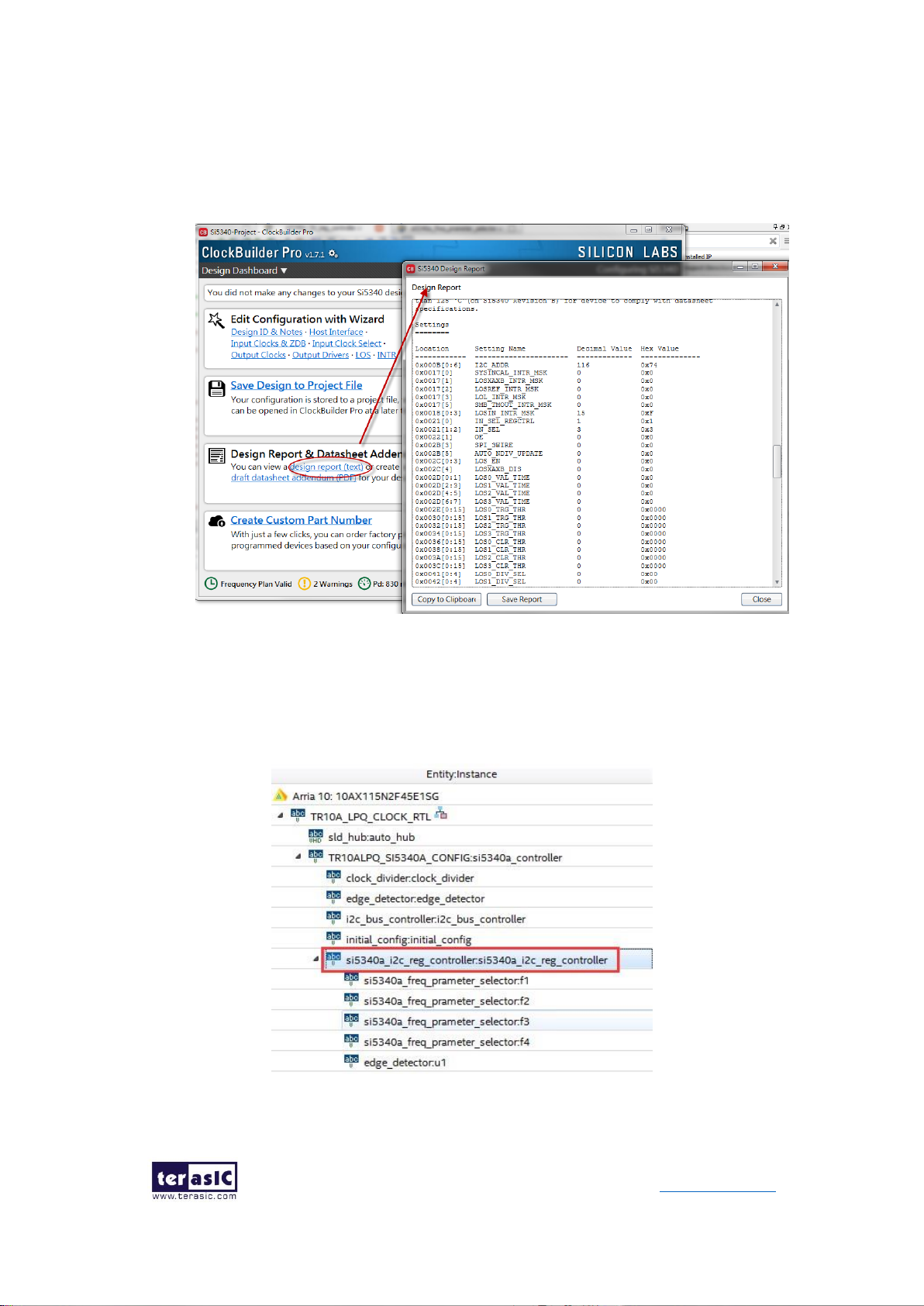
56
TR10a-LPQ User Manual www.terasic.com
December 10,
2018
3. After the setting is completed, ClockBuilder Pro Wizard generates a Design
Report(text), which contains users setting frequency corresponding register
value (See Figure 4-5).
Figure 4-5 Open Design Report on ClockBuilder Pro Wizard
4. Open Si5340A control IP sub-module “si5340a_i2c_reg_controller.v “ as shown
in Figure 4-6, refer Design Report parameter to modify sub-module
corresponding register value (See Figure 4-7).
`
Figure 4-6 Sub-Module file "si5340a_i2c_reg_controller.v"
Page 57

57
TR10a-LPQ User Manual www.terasic.com
December 10,
2018
Figure 4-7 Modify Si5340 Control IP Base on Design Report
After modifying and compiling, Si5340A can output new frequencies according to the
users’ setting.
Note:
1. No need to modify all Design Report parameters in
si5340a_i2c_reg_controller.v, users can ignore parameters which have nothing
to do with the frequency setting
2. After the manually modifying, please remember to modify clock constrain setting
in .SDC file
4.2 Nios II control for SI5340
This demonstration shows how to use the Nios II processor to program the
programmable oscillators (Si5340A) on the FPGA board
◼ System Block Diagram
Figure 4-8 shows the system block diagram of this demonstration. The system requires
a 50 MHz clock provided from the board. Si5340A is controlled by Nios II through the
PIO controller, and programmed through I2C protocol which is implemented in the C
code. The I2C pins from chip are connected to Qsys System Interconnect Fabric
through PIO controllers. The Nios II program toggles the PIO controller to implement
Page 58

58
TR10a-LPQ User Manual www.terasic.com
December 10,
2018
the I2C protocol. The Nios II program is running in the on-chip memory.
Figure 4-8 Block diagram of the Nios II Basic Demonstration
The program provides a menu in nios-terminal, as shown in Figure 4-9 to provide an
interactive interface. With the menu, users can perform the test for Si5340A. Note,
pressing ‘ENTER’ should be followed with the choice number.
Figure 4-9 Menu of Demo Program
In the external PLL(Si5340A) programming test, the program will program the PLL first,
and subsequently will use TERASIC QSYS custom CLOCK_COUNTER IP to count the
clock count in a specified period to check whether the output frequency is changed as
configured. To avoid a Quartus Prime compilation error, dummy transceiver controllers
are created to receive the clock from the external PLL. Users can ignore the functionality
of the transceiver controller in the demonstration. For Si5340A programming, please
Page 59
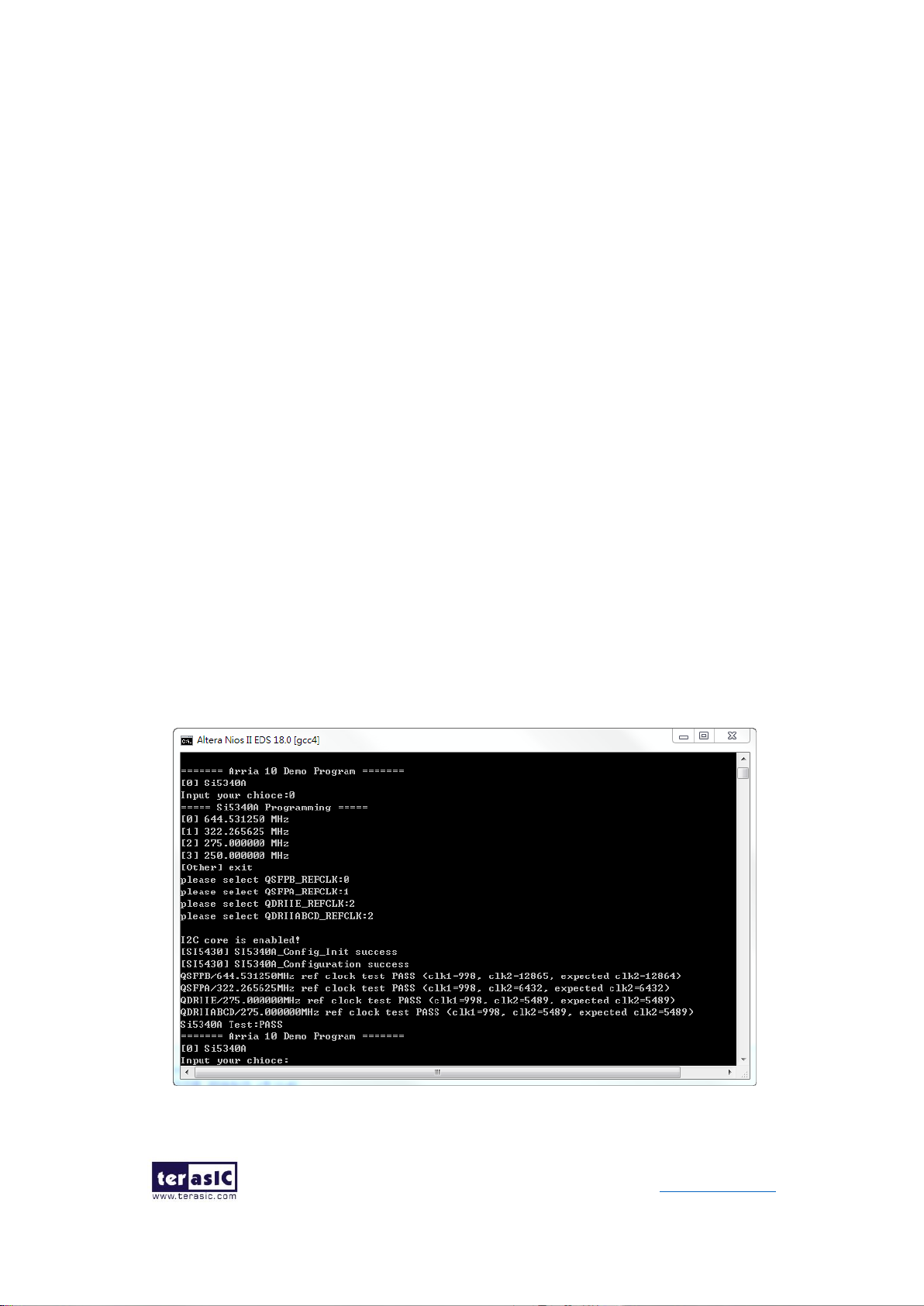
59
TR10a-LPQ User Manual www.terasic.com
December 10,
2018
note the device I2C address are 0xEE. The program can control the Si5340A to
configure the output frequency of QSFPA/B, QDRIIA/B/C/D/E REFCLK.
◼ Demonstration File Locations
⚫ Hardware project directory: NIOS_BASIC_DEMO
⚫ Bitstream used: NIOS_BASIC_DEMO.sof
⚫ Software project directory: NIOS_BASIC_DEMO \software
⚫ Demo batch file: NIOS_BASIC_DEMO\demo_batch\test.bat, test.sh
◼ Demonstration Setup and Instructions
⚫ Make sure Quartus Prime 18.0 and Nios II EDS are installed on your PC.
⚫ Power on the TR10a-LPQ board.
⚫ Use the USB Cable to connect your PC and the FPGA board and install USB
Blaster II driver if necessary.
⚫ Execute the demo batch file “test.bat” under the batch file folder,
NIOS_BASIC_DEMO\demo_batch.
⚫ After the Nios II program is downloaded and executed successfully, a prompt
message will be displayed in nios2-terminal.
⚫ For programmable PLL Si5340A test, please input key “0” and press “Enter” in the
nios-terminal first, then select the desired output frequency of QSFPA/B/C/D
REFCLK, as shown in Figure 4-10.
Figure 4-10 Si5340A Demo
Page 60

60
TR10a-LPQ User Manual www.terasic.com
December 10,
2018
Chapter 5
Memory Reference Design
his chapter will show two examples which use the Altera Memory IP to perform
memory test functions. The source codes of these examples are all available
on the FPGA System CD. These three examples are:
⚫ QDRII+ SRAM Test: Full test of the five banks of QDRII+ SRAM
⚫ QDRII+ SRAM Test by Nios II: Full test of five banks of QDRII+ SRAM with
Nios II
Note. 64-Bit Quartus Prime Standard 18.0 or later is strongly recommended for
compiling these projects.
5.1 QDRII+ SRAM Test
QDR II/QDR II+ SRAM devices enable you to maximize memory bandwidth with
separate read and write ports. The memory architecture features separate read and
write ports operating twice per clock cycle to deliver a total of four data transfers per
cycle. The resulting performance increase is particularly valuable in bandwidth-
intensive and low-latency applications.
This demonstration utilizes five QDRII+ SRAMs on the FPGA board. It describes how
to use Altera’s “Arria 10 External Memory Interfaces” (Arria 10 EMIF) IP to implement a
memory test function.
◼ Function Block Diagram
Figure 5-1 shows the function block diagram of the demonstration. The five QDRII+
SRAM controllers are configured as a 72Mb controller. The QDRII+ SRAM IP generates
a 550MHz clock as memory clock and a half-rate system clock, 275MHz, for the
T
Page 61

61
TR10a-LPQ User Manual www.terasic.com
December 10,
2018
controllers.
Figure 5-1 Function Block Diagram of the QDRII+ SRAM x4 Demonstration
The QDRIIA/B/C/D/E_REFCLK is generated from Si5340A which configured 275MHz
for QDRII+ 550MHz by Clock Config module. QDRIIA/B/C/D/E _REFCLK has no default
frequency output so that they must be configured first.
In this demonstration, each QDRII+ SRAM has its own PLL, DLL and OCT resources.
The Arria 10 EMIF QDRII IP uses a Hard PHY and a soft Controller. The Hard PHY
capable of performing key memory interface functionality such as read/write leveling,
FIFO buffering to lower latency and improve margin, timing calibration, and on-chip
termination.
The Avalon bus read/write test (RW_test) modules read and write the entire memory
space of each QDRII+ SRAM through the Avalon interface of each controller. In this
project, the RW_test module will first write the entire memory and then compare the
Page 62

62
TR10a-LPQ User Manual www.terasic.com
December 10,
2018
read back data with the regenerated data (the same sequence as the write data). Test
control signals for five QDRII+ SRAMs will generate from CPU_RESET_n and four
LEDs will indicate the test results of the first four QDRII+ SRAMs.
◼ Altera QDRII and QDRII+ SRAM Controller with UniPHY
To use Altera QDRII+ SRAM controller, users need to perform the following steps in
order:
1. Create correct pin assignments for QDRII+.
2. Setup correct parameters in QDRII+ SRAM controller dialog.
◼ Design Tools
⚫ Quartus Prime Standard 18.0
◼ Demonstration Source Code
⚫ Project directory: QDRII_x5_Test_550MHz
⚫ Bit stream used: QDRII_x5_Test_550MHz.sof
◼ Demonstration Batch File
Demo Batch File Folder: QDRII_x5_Test_550MHz\demo_batch
The demo batch files include the followings:
⚫ Batch file for USB-Blaster II: test.bat,
⚫ FPGA configuration file: QDRII_x5_Test_550MHz.sof
◼ Demonstration Setup
⚫ Make sure Quartus Prime Standard 18.0 and Nios II EDS are installed on your PC.
⚫ Connect the USB cable to the FPGA board and host PC. Install the USB-Blaster II
driver if necessary.
⚫ Power on the FPGA Board.
⚫ Execute the demo batch file “test.bat” under the batch file folder,
QDRII_x5_Test_550MHz \demo_batch.
⚫ Press CPU_RESET_n of the FPGA board to start the verification process. When
CPU_RESET_n is held down, all the LEDs will be turned off. All LEDs should turn
back on to indicate test passes upon the release of CPU_RESET_n.
⚫ If any LED is not lit up after releasing CPU_RESET_n, it indicates the
Page 63

63
TR10a-LPQ User Manual www.terasic.com
December 10,
2018
corresponding QDRII+ SRAM test has failed. Table 5-1 lists the matchup for the
four LEDs.
⚫ Press CPU_RESET_n again to regenerate the test control signals for a repeat test.
Table 5-1 LED Indicators
NAME
Description
LED0
QDRII+ SRAM(A) test result
LED1
QDRII+ SRAM(B) test result
LED2
QDRII+ SRAM(C) test result
LED3
QDRII+ SRAM(D) test result
5.2 QDRII+ SRAM Test by Nios II
This demonstration hardware and software designs are provided to illustrate how to
perform QDRII+ SRAM memory access in QSYS. We describe how the Altera’s “Arria
10 External Memory Interfaces” IP is used to access the five QDRII+ SRAM on the
FPGA board, and how the Nios II processor is used to read and write the SRAM for
hardware verification. The QDRII+ SRAM controller handles the complex aspects of
using QDRII+ SRAM by initializing the memory devices, managing SRAM banks, and
keeping the devices refreshed at appropriate intervals.
◼ System Block Diagram
Figure 5-2 shows the system block diagram of this demonstration. The QSYS system
requires one 50 MHz and five 550MHz clock source. The five 550MHz clock source is
provided by Si5340A clock generator on the board. Si5340A Config Controller is used
to configure the Si5340A to generate the required clock. The five 550MHz clock are
used as reference clocks for the QDRII+ controllers. There are five QDRII+ Controllers
are used in the demonstrations. Each controller is responsible for one QDRII+ SRAM.
Each QDRII+ controller is configured as a 8 MB QDRII+ controller. Nios II processor is
used to perform memory test. The Nios II program is running in the On-Chip Memory. A
PIO Controller is used to monitor buttons status which is used to trigger starting memory
testing.
Page 64

64
TR10a-LPQ User Manual www.terasic.com
December 10,
2018
Figure 5-2 Block diagram of the QDRII+ Demonstration
The system flow is controlled by a Nios II program. First, the Nios II program writes test
patterns into the whole 8 MB of SRAM. Then, it calls Nios II system function,
alt_dcache_flush_all(), to make sure all data has been written to SRAM. Finally, it reads
data from SRAM for data verification. The program will show progress in JTAG-Terminal
when writing/reading data to/from the SRAM. When verification process is completed,
the result is displayed in the JTAG-Terminal.
◼ Design Tools
⚫ Quartus Prime Standard 18.0.
⚫ Nios II Eclipse 18.0
◼ Demonstration Source Code
⚫ Quartus Project directory: NIOS_QDRII_x5_550
⚫ Nios II Eclipse: NIOS_QDRII_x5_550\software
⚫ Nios II Project Compilation
◼ Nios II Project Compilation
Before you attempt to compile the reference design under Nios II Eclipse, make sure
the project is cleaned first by clicking ‘Clean’ from the ‘Project’ menu of Nios II Eclipse.
Page 65

65
TR10a-LPQ User Manual www.terasic.com
December 10,
2018
◼ Demonstration Batch File
Demo Batch File Folder: NIOS_QDRII_x5_550\demo_batch
The demo batch file includes following files:
⚫ Batch File for USB-Blaster II: test.bat, test.sh
⚫ FPGA Configure File: NIOS_QDRII_x5_550.sof
⚫ Nios II Program: TEST_QDRII.elf
◼ Demonstration Setup
Please follow below procedures to setup the demonstrations.
⚫ Make sure Quartus Prime Standard 18.0 and Nios II 18.0 are installed on your PC.
⚫ Make sure both QDRII+ SRAMs are installed on the FPGA board.
⚫ Power on the FPGA board.
⚫ Use USB Cable to connect PC and the FPGA board and install USB Blaster II
driver if necessary.
⚫ Execute the demo batch file “test.bat” under the folder
“NIOS_QDRII_x5_550\demo_batch”.
⚫ After Nios II program is downloaded and executed successfully, a prompt message
will be displayed in nios2-terminal.
⚫ Press Button1~Button0 of the FPGA board to start SRAM verify process. Press
Button0 for continued test.
⚫ The program will display progressing and result information, as shown in Figure
5-3.
Page 66

66
TR10a-LPQ User Manual www.terasic.com
December 10,
2018
Figure 5-3 Progress and Result Information for the QDRII+ Demonstration
Page 67

67
TR10a-LPQ User Manual www.terasic.com
December 10,
2018
Chapter 6
PCI Express Reference Design
CI Express is commonly used in consumer, server, and industrial applications,
to link motherboard-mounted peripherals. From this demonstration, it will show
how the PC and FPGA communicate with each other through the PCI Express
interface. Arria 10 Hard IP for PCI Express with Avalon-MM DMA IP is used in this
demonstration. For detail about this IP, please refer to Altera document
ug_a10_pcie_avmm_dma.pdf.
6.1 PCI Express System Infrastructure
Figure 6-1 shows the infrastructure of the PCI Express System in this demonstration.
It consists of two primary components: FPGA System and PC System. The FPGA
System is developed based on Arria 10 Hard IP for PCI Express with Avalon-MM DMA.
The application software on the PC side is developed by Terasic based on Altera’s PCIe
kernel mode driver.
P
Page 68

68
TR10a-LPQ User Manual www.terasic.com
December 10,
2018
Figure 6-1 Infrastructure of PCI Express System
6.2 PC PCI Express Software SDK
The FPGA System CD contains a PC Windows based SDK to allow users to develop
their 64-bit software application on Windows 7/Window XP 64-bit. The SDK is located
in the "CDROM \demonstrations\PCIe_SW_KIT" folder which includes:
⚫ PCI Express Driver
⚫ PCI Express Library
⚫ PCI Express Examples
The kernel mode driver assumes the PCIe vender ID (VID) is 0x1172 and the device ID
(DID) is 0xE003. If different VID and DID are used in the design, users need to modify
the PCIe vender ID (VID) and device ID (DID) in the driver INF file accordingly.
The PCI Express Library is implemented as a single DLL named
"TERASIC_PCIE_AVMM.DLL".
This file is a 64-bit DLL. With the DLL is exported to the software API, users can easily
Page 69

69
TR10a-LPQ User Manual www.terasic.com
December 10,
2018
communicate with the FPGA. The library provides the following functions:
⚫ Basic data read and write
⚫ Data read and write by DMA
For high performance data transmission, Altera AVMM DMA is required as the read and
write operations are specified under the hardware design on the FPGA.
6.3 PCI Express Software Stack
Figure 6-2 shows the software stack for the PCI Express application software on 64-bit
Windows. The PCI Express driver incorporated in the DLL library is called
"TERASIC_PCIE_AVMM.dll". Users can develop their applications based on this DLL.
The "altera_pcie_win_driver.sys" kernel driver is provided by Altera.
Figure 6-2 PCI Express Software Stack
Page 70

70
TR10a-LPQ User Manual www.terasic.com
December 10,
2018
◼ Install PCI Express Driver on Windows
The PCIe driver is locate in the folder:
CDROM\Demonstrations\PCIe_SW_KIT\Windows\PCIe_Driver
The folder includes the following four files:
⚫ Altera_pcie_win_driver.cat
⚫ Altera_pcie_win_driver.inf
⚫ Altera_pcie_win_driver.sys
⚫ WdfCoinstaller01011.dll
To install the PCI Express driver, please execute the steps below:
1. Install the TR10a-LPQ on the PCIe slot of the host PC
2. Make sure Altera Programmer and USB-Blaster II driver are installed
3. Execute test.bat in "CDROM\Demonstrations\PCIe_Fundamental\demo_batch"
to configure the FPGA
4. Restart windows operation system
5. Click Control Panel menu from Windows Start menu. Click Hardware and Sound
item before clicking the Device Manager to launch the Device Manager dialog.
There will be a PCI Device item in the dialog, as shown in Figure 6-3. Move the
mouse cursor to the PCI Device item and right click it to select the Update Driver
Software... item.
Page 71

71
TR10a-LPQ User Manual www.terasic.com
December 10,
2018
Figure 6-3 Screenshot of launching Update Driver Software… dialog
6. In the How do you want to search for driver software dialog, click Browse
my computer for driver software item, as shown in Figure 6-4.
Figure 6-4 Dialog of Browse my computer for driver software
7. In the Browse for driver software on your computer dialog, click the Browse
Page 72

72
TR10a-LPQ User Manual www.terasic.com
December 10,
2018
button to specify the folder where altera_pcie_din_driver.inf is located, as shown
in Figure 6-5. Click the Next button.
Figure 6-5 Browse for driver software on your computer
8. When the Windows Security dialog appears, as shown Figure 6-6, click the
Install button.
Figure 6-6 Click Install in the dialog of Windows Security
Page 73

73
TR10a-LPQ User Manual www.terasic.com
December 10,
2018
9. When the driver is installed successfully, the successfully dialog will appears, as
shown in Figure 6-7. Click the Close button.
Figure 6-7 Click Close when the installation of Altera PCI API Driver is complete
Page 74

74
TR10a-LPQ User Manual www.terasic.com
December 10,
2018
Once the driver is successfully installed, users can see the Altera PCI API Driver
under the device manager window, as shown in Figure 6-8.
Figure 6-8 Altera PCI API Driver in Device Manager
◼ Create a Software Application
All the files needed to create a PCIe software application are located in the directory
CDROM\demonstration\PCIe_SW_KIT\PCIe_Library. It includes the following files:
⚫ TERASIC_PCIE_AVMM.h
⚫ TERASIC_PCIE_AVMM.DLL (64-bit DLL)
Below lists the procedures to use the SDK files in users’ C/C++ project :
1. Create a 64-bit C/C++ project.
2. Include "TERASIC_PCIE_AVMM.h" in the C/C++ project.
3. Copy "TERASIC_PCIE_AVMM.DLL" to the folder where the project.exe is located.
4. Dynamically load "TERASIC_PCIE_AVMM.DLL" in C/C++ program. To load the
DLL, please refer to the PCIe fundamental example below.
5. Call the SDK API to implement the desired application.
Users can easily communicate with the FPGA through the PCIe bus through the
"TERASIC_PCIE_AVMM.DLL" API. The details of API are described below:
Page 75

75
TR10a-LPQ User Manual www.terasic.com
December 10,
2018
◼ PCIE_Open
Function:
Open a specified PCIe card with vendor ID, device ID, and matched card index.
Prototype:
PCIE_HANDLE PCIE_Open(
WORD wVendorID,
WORD wDeviceID,
WORD wCardIndex);
Parameters:
wVendorID:
Specify the desired vendor ID. A zero value means to ignore the vendor ID.
wDeviceID:
Specify the desired device ID. A zero value means to ignore the device ID.
wCardIndex:
Specify the matched card index, a zero based index, based on the matched verder
ID and device ID.
Return Value:
Return a handle to presents specified PCIe card. A positive value is return if the PCIe
card is opened successfully. A value zero means failed to connect the target PCIe
card.
This handle value is used as a parameter for other functions, e.g. PCIE_Read32.
Users need to call PCIE_Close to release handle once the handle is no more used.
◼ PCIE_Close
Function:
Close a handle associated to the PCIe card.
Prototype:
void PCIE_Close(
PCIE_HANDLE hPCIE);
Parameters:
hPCIE:
A PCIe handle return by PCIE_Open function.
Return Value:
None.
◼ PCIE_Read32
Function:
Page 76

76
TR10a-LPQ User Manual www.terasic.com
December 10,
2018
Read a 32-bit data from the FPGA board.
Prototype:
bool PCIE_Read32(
PCIE_HANDLE hPCIE,
PCIE_BAR PcieBar,
PCIE_ADDRESS PcieAddress,
DWORD * pdwData);
Parameters:
hPCIE:
A PCIe handle return by PCIE_Open function.
PcieBar:
Specify the target BAR.
PcieAddress:
Specify the target address in FPGA.
pdwData:
A buffer to retrieve the 32-bit data.
Return Value:
Return TRUE if read data is successful; otherwise FALSE is returned.
◼ PCIE_Write32
Function:
Write a 32-bit data to the FPGA Board.
Maximal write size is (4GB-1) bytes.
Prototype:
bool PCIE_Write32(
PCIE_HANDLE hPCIE,
PCIE_BAR PcieBar,
PCIE_ADDRESS PcieAddress,
DWORD dwData);
Page 77

77
TR10a-LPQ User Manual www.terasic.com
December 10,
2018
Parameters:
hPCIE:
A PCIe handle return by PCIE_Open function.
PcieBar:
Specify the target BAR.
PcieAddress:
Specify the target address in FPGA.
dwData:
Specify a 32-bit data which will be written to FPGA board.
Return Value:
Return TRUE if write data is successful; otherwise FALSE is returned.
◼ PCIE_DmaRead
Function:
Read data from the memory-mapped memory of FPGA board in DMA.
Maximal read size is (4GB-1) bytes.
Prototype:
bool PCIE_DmaRead(
PCIE_HANDLE hPCIE,
PCIE_LOCAL_ADDRESS LocalAddress,
void *pBuffer,
DWORD dwBufSize
);
Parameters:
hPCIE:
A PCIe handle return by PCIE_Open function.
LocalAddress:
Specify the target memory-mapped address in FPGA.
pBuffer:
A pointer to a memory buffer to retrieved the data from FPGA. The size of buffer
should be equal or larger the dwBufSize.
dwBufSize:
Specify the byte number of data retrieved from FPGA.
Return Value:
Return TRUE if read data is successful; otherwise FALSE is returned.
◼ PCIE_DmaWrite
Page 78

78
TR10a-LPQ User Manual www.terasic.com
December 10,
2018
Function:
Write data to the memory-mapped memory of FPGA board in DMA.
Prototype:
bool PCIE_DmaWrite(
PCIE_HANDLE hPCIE,
PCIE_LOCAL_ADDRESS LocalAddress,
void *pData,
DWORD dwDataSize
);
Parameters:
hPCIE:
A PCIe handle return by PCIE_Open function.
LocalAddress:
Specify the target memory mapped address in FPGA.
pData:
A pointer to a memory buffer to store the data which will be written to FPGA.
dwDataSize:
Specify the byte number of data which will be written to FPGA.
Return Value:
Return TRUE if write data is successful; otherwise FALSE is returned.
◼ PCIE_ConfigRead32
Function:
Read PCIe Configuration Table. Read a 32-bit data by given a byte offset.
Prototype:
bool PCIE_ConfigRead32 (
PCIE_HANDLE hPCIE,
DWORD Offset,
DWORD *pdwData
);
Parameters:
hPCIE:
A PCIe handle return by PCIE_Open function.
Offset:
Specify the target byte of offset in PCIe configuration table.
pdwData:
A 4-bytes buffer to retrieve the 32-bit data.
Page 79

79
TR10a-LPQ User Manual www.terasic.com
December 10,
2018
Return Value:
Return TRUE if read data is successful; otherwise FALSE is returned.
6.4 PCIe Design - Fundamental
The application reference design shows how to implement fundamental control and data
transfer in DMA. In the design, basic I/O is used to control the BUTTON and LED on
the FPGA board. High-speed data transfer is performed by DMA.
◼ Demonstration Files Location
The demo file is located in the batch folder:
CDROM\demonstrations\PCIe_fundamental\demo_batch
The folder includes following files:
⚫ FPGA Configuration File: PCIe_Fundamental.sof
⚫ Download Batch file: test.bat
⚫ Windows Application Software folder : windows_app, includes
PCIE_FUNDAMENTAL.exe
TERASIC_PCIE_AVMM.dll
◼ Demonstration Setup
1. Install the FPGA board on your PC as shown in Figure 6-9.
Figure 6-9 FPGA board installation on PC
2. Configure FPGA with PCIe_Fundamental.sof by executing the test.bat.
3. Install PCIe driver if necessary. The driver is located in the folder:
Page 80

80
TR10a-LPQ User Manual www.terasic.com
December 10,
2018
CDROM\Demonstration\PCIe_SW_KIT\PCIe_Driver
4. Restart Windows
5. Make sure the Windows has detected the FPGA Board by checking the Windows
Control panel as shown in Figure 6-10.
Figure 6-10 Screenshot for PCIe Driver
6. Goto windows_app folder, execute PCIE_FUNDMENTAL.exe. A menu will appear
as shown in Figure 6-11.
Page 81

81
TR10a-LPQ User Manual www.terasic.com
December 10,
2018
Figure 6-11 Screenshot of Program Menu
7. Type 0 followed by a ENTERY key to select Led Control item, then input 15 (hex
0x0f) will make all led on as shown in Figure 6-12. If input 0(hex 0x00), all led will
be turn off.
Page 82

82
TR10a-LPQ User Manual www.terasic.com
December 10,
2018
Figure 6-12 Screenshot of LED Control
8. Type 1 followed by an ENTERY key to select Button Status Read item. The button
status will be report as shown in Figure 6-13.
Figure 6-13 Screenshot of Button Status Report
9. Type 2 followed by an ENTERY key to select DMA Testing item. The DMA test result
will be report as shown in Figure 6-14.
Page 83

83
TR10a-LPQ User Manual www.terasic.com
December 10,
2018
Figure 6-14 Screenshot of DMA Memory Test Result
10. Type 99 followed by an ENTERY key to exit this test program
◼ Development Tools
⚫ Quartus Prime Standard 18.0
⚫ Visual C++ 2012
◼ Demonstration Source Code Location
⚫ Quartus Project: Demonstrations\PCIe_Fundamental
⚫ Visual C++ Project: Demonstrations\PCIe_SW_KIT\PCIE_FUNDAMENTAL
◼ FPGA Application Design
Figure 6-15 shows the system block diagram in the FPGA system. In the Qsys, Altera
PIO controller is used to control the LED and monitor the Button Status, and the On-
Chip memory is used for performing DMA testing. The PIO controllers and the On-Chip
memory are connected to the PCI Express Hard IP controller through the Memory-
Mapped Interface.
Page 84

84
TR10a-LPQ User Manual www.terasic.com
December 10,
2018
Figure 6-15 Hardware block diagram of the PCIe reference design
◼ Windows Based Application Software Design
The application software project is built by Visual C++ 2012. The project includes the
following major files:
Name
Description
PCIE_FUNDAMENTAL.cpp
Main program
PCIE.c
Implement dynamically load for
TERAISC_PCIE_AVMM.DLL
PCIE.h
TERASIC_PCIE_AVMM.h
SDK library file, defines constant and data structure
The main program PCIE_FUNDAMENTAL.cpp includes the header file "PCIE.h" and
defines the controller address according to the FPGA design.
Page 85

85
TR10a-LPQ User Manual www.terasic.com
December 10,
2018
The base address of BUTTON and LED controllers are 0x4000010 and 0x4000020
based on PCIE_BAR4, in respectively. The on-chip memory base address is
0x00000000 relative to the DMA controller.
Before accessing the FPGA through PCI Express, the application first calls PCIE_Load
to dynamically load the TERASIC_PCIE_AVMM.DLL. Then, it call PCIE_Open to open
the PCI Express driver. The constant DEFAULT_PCIE_VID and DEFAULT_PCIE_DID
used in PCIE_Open are defined in TERASIC_PCIE_AVMM.h.If developer change the
Vender ID and Device ID and PCI Express IP, they also need to change the ID value
define in TERASIC_PCIE_AVMM.h. If the return value of PCIE_Open is zero, it means
the driver cannot be accessed successfully. In this case, please make sure:
⚫ The FPGA is configured with the associated bit-stream file and the host is rebooted.
⚫ The PCI express driver is loaded successfully.
The LED control is implemented by calling PCIE_Write32 API, as shown below:
The button status query is implemented by calling the PCIE_Read32 API, as shown
below:
The memory-mapped memory read and write test is implemented by PCIE_DmaWrite
and PCIE_DmaRead API, as shown below:
Page 86

86
TR10a-LPQ User Manual www.terasic.com
December 10,
2018
6.5 PCIe Design – QDRII+
The application reference design shows how to add QDRII+ Memory Controllers for five
QDRII+ SRAMs into the PCIe Quartus project based on the PCI_Fundamental Quartus
project and perform 8MB data DMA for five SRAMs. Also, this demo shows how to call
"PCIE_ConfigRead32" API to check PCIe link status.
◼ Demonstration Files Location
The demo file is located in the batch folder:
CDROM\demonstrations\PCIe_QDR\demo_batch
The folder includes following files:
⚫ FPGA Configuration File: PCIe_QDR.sof
⚫ Download Batch file: test.bat
⚫ Windows Application Software folder : windows_app, includes
PCIE_QDR.exe
TERASIC_PCIE_AVMM.dll
◼ Demonstration Setup
1. Install the FPGA board on your PC.
2. Configure FPGA with PCIe_QDR.sof by executing the test.bat.
3. Install PCIe driver if necessary.
4. Restart Windows
5. Make sure the Windows has detected the FPGA Board by checking the Windows
Control panel.
6. Goto windows_app folder, execute PCIE_QDR.exe. A menu will appear as shown
in Figure 6-16.
Page 87

87
TR10a-LPQ User Manual www.terasic.com
December 10,
2018
Figure 6-16 Screenshot of Program Menu
7. Type 2 followed by a ENTERY key to select Link Info item. The PICe link information
will be shown as in Figure 6-17. Gen3 link speed and x8 link width are expected.
Figure 6-17 Screenshot of Link Info
Page 88

88
TR10a-LPQ User Manual www.terasic.com
December 10,
2018
8. Type 3 followed by an ENTERY key to select DMA On-Chip Memory Test item. The
DMA write and read test result will be report as shown in Figure 6-18.
Figure 6-18 Screenshot of On-Chip Memory DMA Test Result
9. Type 4 followed by an ENTERY key to select DMA QDRII-A Memory Test item. The
DMA write and read test result will be report as shown in Figure 6-19.
Page 89

89
TR10a-LPQ User Manual www.terasic.com
December 10,
2018
Figure 6-19 Screenshot of QDRII-A Memory DAM Test Result
10. Type 5 followed by an ENTERY key to select DMA QDRII-B Memory Test item. The
DMA write and read test result will be report as shown in Figure 6-20.
Page 90

90
TR10a-LPQ User Manual www.terasic.com
December 10,
2018
Figure 6-20 Screenshot of QDRII-B Memory DAM Test Result
11. Type 6 followed by an ENTERY key to select DMA QDRII-C Memory Test item. The
DMA write and read test result will be report as shown in Figure 6-21.
Page 91

91
TR10a-LPQ User Manual www.terasic.com
December 10,
2018
Figure 6-21 Screenshot of QDRII-C Memory DAM Test Result
12. Type 7 followed by an ENTERY key to select DMA QDRII-D Memory Test item. The
DMA write and read test result will be report as shown in Figure 6-22.
Page 92

92
TR10a-LPQ User Manual www.terasic.com
December 10,
2018
Figure 6-22 Screenshot of QDRII-D Memory DAM Test Result
13. Type 8 followed by an ENTERY key to select DMA QDRII-E Memory Test item. The
DMA write and read test result will be report as shown in Figure 6-23.
Page 93

93
TR10a-LPQ User Manual www.terasic.com
December 10,
2018
Figure 6-23 Screenshot of QDRII-E Memory DAM Test Result
14. Type 99 followed by an ENTERY key to exit this test program.
◼ Development Tools
⚫ Quartus Prime Standard 18.0
⚫ Visual C++ 2012
◼ Demonstration Source Code Location
⚫ Quartus Project: Demonstrations\PCIE_QDR
⚫ Visual C++ Project: Demonstrations\PCIe_SW_KIT\PCIE_QDR
◼ FPGA Application Design
Figure 6-24 shows the system block diagram in the FPGA system. In the Qsys, Altera
PIO controller is used to control the LED and monitor the Button Status, and the On-
Chip memory is used for performing DMA testing. The PIO controllers and the On-Chip
memory are connected to the PCI Express Hard IP controller through the Memory-
Mapped Interface.
Page 94

94
TR10a-LPQ User Manual www.terasic.com
December 10,
2018
Figure 6-24 Hardware block diagram of the PCIe QDRII+ reference design
◼ Windows Based Application Software Design
The application software project is built by Visual C++ 2012. The project includes the
following major files:
Name
Description
PCIE_QDR.cpp
Main program
PCIE.c
Implement dynamically load for
TERAISC_PCIE_AVMM.DLL
PCIE.h
TERASIC_PCIE_AVMM.h
SDK library file, defines constant and data structure
The main program PCIE_QDR.cpp includes the header file "PCIE.h" and defines the
controller address according to the FPGA design.
Page 95

95
TR10a-LPQ User Manual www.terasic.com
December 10,
2018
The base address of BUTTON and LED controllers are 0x4000010 and 0x4000020
based on PCIE_BAR4, in respectively. The on-chip memory base address is
0x00000000 relative to the DMA controller. The above definition is the same as those
in PCIe Fundamental demo.
Before accessing the FPGA through PCI Express, the application first calls PCIE_Load
to dynamically load the TERASIC_PCIE_AVMM.DLL. Then, it call PCIE_Open to open
the PCI Express driver. The constant DEFAULT_PCIE_VID and DEFAULT_PCIE_DID
used in PCIE_Open are defined in TERASIC_PCIE_AVMM.h. If developer change the
Vender ID and Device ID and PCI Express IP, they also need to change the ID value
define in TERASIC_PCIE_AVMM.h. If the return value of PCIE_Open is zero, it means
the driver cannot be accessed successfully. In this case, please make sure:
⚫ The FPGA is configured with the associated bit-stream file and the host is rebooted.
⚫ The PCI express driver is loaded successfully.
The LED control is implemented by calling PCIE_Write32 API, as shown below:
The button status query is implemented by calling the PCIE_Read32 API, as shown
below:
Page 96

96
TR10a-LPQ User Manual www.terasic.com
December 10,
2018
The memory-mapped memory read and write test is implemented by PCIE_DmaWrite
and PCIE_DmaRead API, as shown below:
The pcie link information is implemented by PCIE_ConfigRead32 API, as shown below:
Page 97

97
TR10a-LPQ User Manual www.terasic.com
December 10,
2018
6.6 PCIe Design: PCIe_Fundamental_x2
The application reference design shows how to utilize the dual PCIe Gen3 x8 edge
connector on this board. The two PCIe Gen3 x8 Link are directly connected to two Arria
10 PCIe Hard IP individually. There two IP are call PCIe0 and PCIe1 in this design.
The Host PC can communicated with the two Hard IP independently, so the throughput
between Host PC and FPGA is double than the single PCIe Gen3 x8 link. In the design,
basic I/O is used to control the BUTTON and LED on the FPGA board. PCIe0 controls
the User LED and PCIe1 controls the Bracket LED. High-speed data transfer is
performed by DMA.
Note, this demonstration requires the Host PC to support PCIe Bifurcation.
◼ Demonstration Files Location
The demo file is located in the batch folder:
CDROM\demonstrations\PCIe_funcdamental_x2\demo_batch
The folder includes following files:
⚫ FPGA Configuration File: PCIe_Fundamental_x2.sof
⚫ Download Batch file: test.bat
⚫ Windows Application Software folder : windows_app, includes
PCIE_FUNDAMENTAL.exe
TERASIC_PCIE_AVMM.dll
◼ Demonstration Setup
1. Make sure your Host PC supports PCIe bifurcation and is enabled in BIOS.
2. Install the FPGA board on the bifurcation PCIe slot of your PC.
3. Configure FPGA with PCIe_Fundamental_x2.sof by executing the test.bat.
4. Install PCIe driver if necessary. The driver is located in the folder:
CDROM\Demonstration\PCIe_SW_KIT\PCIe_Driver
5. Restart Windows
6. Make sure there are two Altera PCI API drivers are enumerated by checking the
Windows Control panel as shown in Figure 6-25.
7. Goto windows_app folder, execute PCIE_FUNDMENTAL.exe. A menu will appear
as shown in Figure 6-26.
Page 98

98
TR10a-LPQ User Manual www.terasic.com
December 10,
2018
Figure 6-25 Screenshot of two FPGA PCIe devices are detected
Figure 6-26 Screenshot of Program Menu
8. Type 0 followed by a ENTERY key to select PCIe0 Led Control item, then input 15
(hex 0x0f) will make all User LED lighten as shown in Figure 6-27. If input 0(hex
0x00), all User LED will be turn off.
Page 99
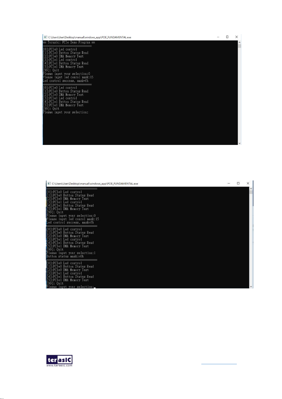
99
TR10a-LPQ User Manual www.terasic.com
December 10,
2018
Figure 6-27 Screenshot of PCIe0 LED Control
9. Type 1 followed by an ENTERY key to select PCIe0 Button Status Read item. The
button status will be report as shown in Figure 6-28.
Figure 6-28 Screenshot of PCIe0 Button Status Report
10. Type 2 followed by an ENTERY key to select PCIe0 DMA Testing item. The DMA
test result will be report as shown in Figure 6-29.
Page 100

100
TR10a-LPQ User Manual www.terasic.com
December 10,
2018
Figure 6-29 Screenshot of PCIe0 DMA Memory Test Result
11. Type 3 followed by a ENTERY key to select PCIe1 Led Control item, then input 15
(hex 0x0f) will make all Bracket LED on as shown in Figure 6-30. If input 0(hex
0x00), all Bracket LED will be turn off.
Figure 6-30 Screenshot of PCIe1 LED Control
12. Type 4 followed by an ENTERY key to select PCIe1 Button Status Read item. The
button status will be report as shown in Figure 6-31.
 Loading...