

Page 1
Terasic THDB-HTG
THDB-HTG
Terasic HSTC to GPIO Daughter Board
User Manual
Document Version 1.0 DEC. 23, 2008 by Terasic
Page 2

Introduction
ii
Page Index
INTRODUCTION..........................................................................................................................................................1
1-1 FEATURES...................................................................................................................................................................................1
1-2 GETTING HELP ........................................................................................................................................................................... 1
ARCHITECTURE.........................................................................................................................................................2
1-3 LAYOUT AND COMPONETS.......................................................................................................................................................... 2
1-4 BLOCK DIAGRAM ........................................................................................................................................................................ 4
BOARD COMPONENTS.............................................................................................................................................5
1-5 HSTC/HSMC EXPANSION CONNECTOR................................................................................................................................... 5
1-6 EXPANSION PROTOTYPE CONNECTORS.................................................................................................................................... 7
1-7 PROTOTYPING AREA ................................................................................................................................................................ 12
1-8 JTAG SWITCH.......................................................................................................................................................................... 13
1-9 POWER ON CONTROL PIN....................................................................................................................................................... 13
1-10 I2C SERIAL EEPROM........................................................................................................................................................... 13
1-11 POWER SUPPLY...................................................................................................................................................................... 14
DEMONSTRATION....................................................................................................................................................15
1-12 CONNECTING THDB-HTG BOARD TO A CYCLONE III STARTER BOARD .............................................................................. 15
1-13 CONNECTING THDB-HTG BOARD TO ALTERA DE3 BOARD ................................................................................................ 16
APPENDIX ..................................................................................................................................................................17
1-14 MECHANICAL.......................................................................................................................................................................... 17
1-15 REVISION HISTORY ................................................................................................................................................................ 17
1-16 ALWAYS VISIT THDB-HTG WEBPAG E FOR NEW MAIN BOARD.............................................................................................17
Page 3
Introduction
1
Introduction
1
The THDB-HTG board is designed to convert a High-Speed Terasic connector (HSTC) or a High-Speed
Mezzanine connector (HSMC) I/Os to three 40-pin expansion prototype connectors, which are compatible
with Altera DE2/DE1 expansion headers. Users can connect up to three Altera DE2/DE1 boards (or
associated daughter cards) onto a HSTC/HSMC-interfaced host board via a THDB-HTG board.
1-1Features
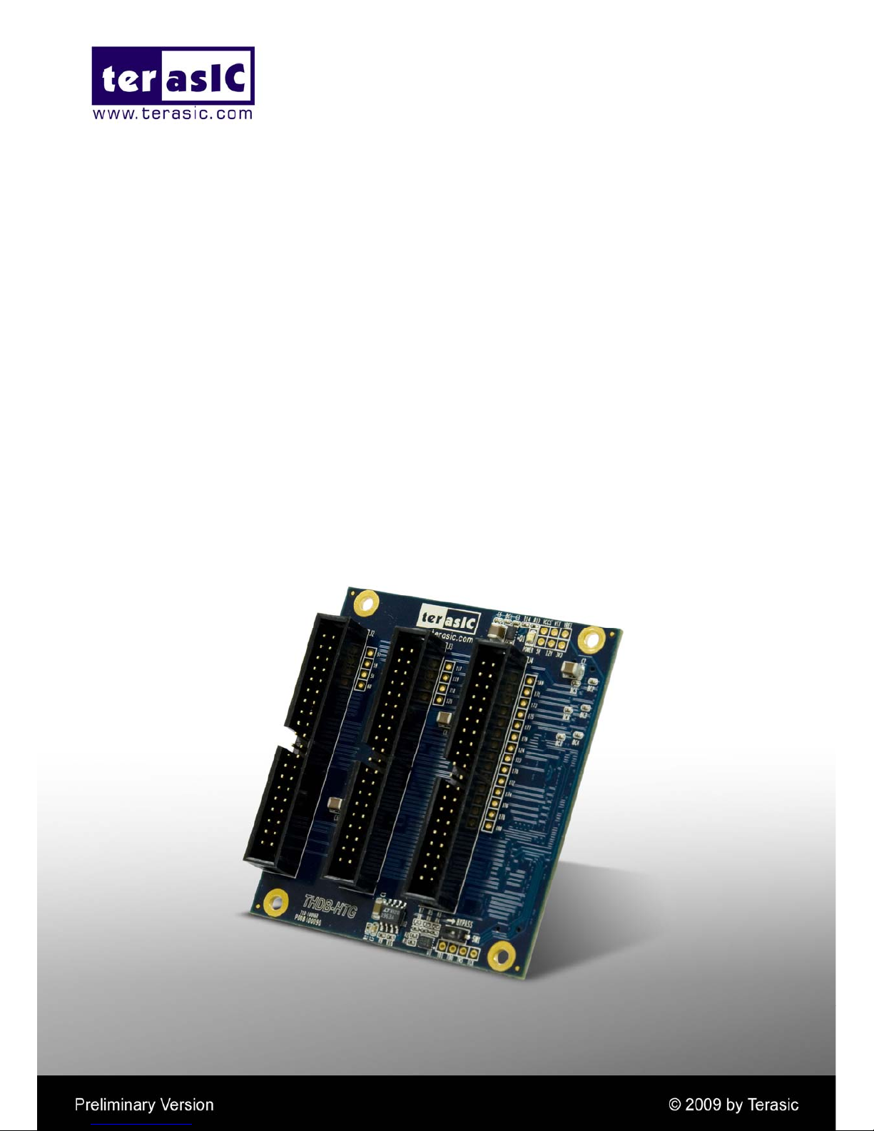
Figure 1.1 shows the photo of a THDB-HTG board. The impo rtant functions of the THDB-HTG are listed
below:
• Convert HSTC/HSMC-interfaced I/O to standard 40-pin expansion connectors.
• Allow users to connect Altera DE2/DE1 boards to a HSTC/HSMC-interfaced host board.
• Provide test points for signal measurement.
Figure 1.1. The picture of a THDB-HTG board
1-2Getting Help
Here are some places to get help if you encounter any problem:
9 Email to support@terasic.com
9 Taiwan & China: +886-3-550-8800
9 Korea : +82-2-512-7661
9 English Support Line: +1-408-512-12336
Page 4
Architecture
2
Architecture
2
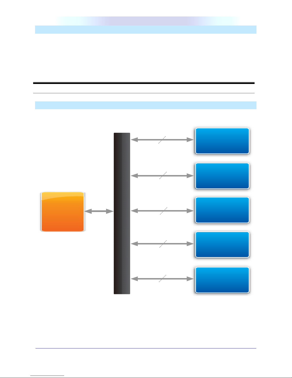
This chapter describes the architecture of the THDB-HTG board, including block diagram and components.
1-3Layout and Componets
Figure 2.1, Figure 2.2, and Figure 2.3 depict the layout of the board and indicate the locations of the connector s
nd key components.
Expansion
Prototype
Connector (J2)
Expansion
Prototype
Connector (J3)
Expansion
Prototype
Connector (J4)
Prototype
Area
Prototype
Area
I2C Serial
EEPROM(U1)
JTAG
Switch (SW1)
Figure 2.1 Top view of the TDRB-HTG board
Page 5
Architecture
3
180-pin Female
HSTC Connector
(J1)
Figure 2.2 Back side of the TDRB-HTG board – HSTC version
180-pin Male
HSMC
Connector (J1)
Figure 2.3 Back side of the TDRB-HTG board – HSMC version
Page 6
Architecture
4
The following components are provided on the THDB-HTG b oard :
• HSTC/HSMC expansion connector (J1)
• Expansion prototype connectors (J2,J3,J4)
• I2C serial EEPROM (U1)
1-4Block Diagram
Figure 2.4 shows the block diagram of the THDB-HTG board.
To HSTC/HSMC
Interface
Host Board
HSTC/HSMC
Connector
40-Pin Expansion
Prototype Connector 1
J2
40-Pin Expansion
Prototype Connector 3
J4
Prototype Area
40-Pin Expansion
Prototype Connector 2
J3
I2C Serial EEPRO M
U1
36 I/Os
36 I/Os
36 I/Os
22 I/Os
I2C Interface
J1
Figure 2.4. The block diagram of the THDB-HTG board
Page 7

Board Components
5
Board Components
3
This section will describe the information of components, connector interfaces, and pin
mappings on the THDB-HTG board in details.
1-5HSTC/HSMC Expansion Connector
This section describes the HSTC/HSMC connector on the THDB-HTG b oard
There are two options of high speed connector on the THDB-HTG board. One is a 180-pin female HSTC
connector for HSTC-interfaced host board such as Altera DE3 board and Terasic PCI board. The other one is
a 180-pin male connector for Altera HSMC-interfa ced host board. All other interfaces on the THDB-HTG board
are connected to the HSTC/HSMC connector. Figure 3.1 shows the pin-outs of the HSTC and HSMC
connector.
Page 8

Board Components
6
2
2
4
4 HSTCA_CLKIN_n0
HSTCA_CLKIN_p0
HSTCA_RX_n0
HSTCA_RX_p0
HSTCA_RX_n1
HSTCA_RX_p1
HSTCA_RX_n2
HSTCA_RX_p2
HSTCA_RX_n3
HSTCA_RX_p3
HSTCA_RX_n4
HSTCA_RX_p4
HSTCA_RX_n5
HSTCA_RX_p5
HSTCA_RX_n6
HSTCA_RX_p6
HSTCA_RX_n7
HSTCA_RX_p7
HSTCA_RX_n8
HSTCA_RX_p8
6
6
8
8
10
10
12
12
14
14
16
16
18
18
20
20
22
22
24
24
26
26
28
28
30
30
32
32
34
34
36
36
38
38
40
40
42
42
44
44
46
46
48
48
50
50
52
52
54
54
56
56
58
58
60
60
HSTCA_CLKIN_n1
64
64
HSTCA_CLKIN_p1
66
66
HSTCA_RX_n9
70
70
HSTCA_RX_p9
72
72
62
62
68
68
HSTCA_RX_n10
76
76
HSTCA_RX_p10
78
78
74
74
HSTCA_RX_n11
82
82
HSTCA_RX_p11
84
84
80
80
HSTCA_RX_n12
88
88
HSTCA_RX_p12
90
90
86
86
HSTCA_RX_n13
94
94
HSTCA_RX_p13
96
96
92
92
HSTCA_RX_n14
100
100
HSTCA_RX_p14
102
102
98
98
HSTCA_RX_n15
106
106
HSTCA_RX_p15
108
108
104
104
HSTCA_RX_n16
112
112
HSTCA_RX_p16
114
114
110
110
HSTCA_RX_n17
118
118
HSTCA_RX_p17
120
120
122
122
HSTCA_CLKIN_2
VCC50
BA_VTT
124
124
124
HSTCA_TDI
HSTCA_TMS
126
126
128
128
130
130
HSTCA_SCL
132
132
HSTCA_RX_n18
134
134
HSTCA_RX_p18
136
136
HSTCA_RX_n19
138
138
HSTCA_RX_p19
140
140
HSTCA_RX_n20
142
142
HSTCA_RX_p20
144
144
HSTCA_RX_n21
146
146
HSTCA_RX_p21
148
148
HSTCA_RX_n22
150
150
HSTCA_RX_p22
152
152
HSTCA_RX_n23
154
154
HSTCA_RX_p23
156
156
HSTCA_RX_n24
158
158
HSTCA_RX_p24
160
160
HSTCA_RX_n25
162
162
HSTCA_RX_p25
164
164
HSTCA_RX_n26
166
166
HSTCA_RX_p26
168
168
HSTCA_RX_n27
170
116
116
1
3
5
7
9
11
13
15
17
19
21
23
25
27
39
31
33
35
37
39
41
43
45
47
49
51
53
55
57
59
63
65
69
71
61
67
75
77
73
81
83
79
87
89
85
93
95
91
99
101
97
105
107
103
111
113
109
117
119
121
123
125
127
129
131
133
135
137
139
141
143
145
147
149
151
153
155
157
159
161
163
165
167
115
1
3
5
7
9
11
13
15
17
19
21
23
25
27
39
31
33
35
37
39
41
43
45
47
49
51
53
55
57
59
63
65
69
71
61
67
75
77
73
81
83
79
87
89
85
93
95
91
99
101
97
105
107
103
111
113
109
117
119
121
123
125
127
129
131
133
135
137
139
141
143
145
147
149
151
153
155
157
159
161
163
165
167
115
HSTCA_CLKOUT_n0
VCC33
12V
J1
HSTCA_CLKOUT_p0
HSTCA_TX_n0
HSTCA_TX_p0
HSTCA_TX_n1
HSTCA_TX_p1
HSTCA_TX_n2
HSTCA_TX_p2
HSTCA_TX_n3
HSTCA_TX_p3
HSTCA_TX_n4
HSTCA_TX_p4
HSTCA_TX_n5
HSTCA_TX_p5
HSTCA_TX_n6
HSTCA_TX_p6
HSTCA_TX_n7
HSTCA_TX_p7
HSTCA_TX_n8
HSTCA_TX_p8
HSTCA_CLKOUT_n1
HSTCA_CLKOUT_p1
HSTCA_TX_n9
HSTCA_TX_p9
HSTCA_TX_n10
HSTCA_TX_p10
HSTCA_TX_n11
HSTCA_TX_p11
HSTCA_TX_n12
HSTCA_TX_p12
HSTCA_TX_n13
HSTCA_TX_p13
HSTCA_TX_n14
HSTCA_TX_p14
HSTCA_TX_n15
HSTCA_TX_p15
HSTCA_TX_n16
HSTCA_TX_p16
HSTCA_TX_n17
HSTCA_TX_p17
HSTCA_CLKOUT_2
POWER ON
BA_VREF
HSTCA_TDO
HSTCA_TCK
HSTCA_SDA
HSTCA_TX_n18
HSTCA_TX_p18
HSTCA_TX_n19
HSTCA_TX_p19
HSTCA_TX_n20
HSTCA_TX_p20
HSTCA_TX_n21
HSTCA_TX_p21
HSTCA_TX_n22
HSTCA_TX_p22
HSTCA_TX_n23
HSTCA_TX_p23
HSTCA_TX_n24
HSTCA_TX_p24
HSTCA_TX_n25
HSTCA_TX_p25
HSTCA_TX_n26
HSTCA_TX_p26
170
HSTCA_RX_p27
172
172
HSTCA_RX_n28
174
174
HSTCA_RX_p28
176
176
HSTCA_RX_n29
178
178
HSTCA_RX_p29
180
180
169
171
173
175
177
179
169
171
173
175
177
179
HSTCA_TX_n27
HSTCA_TX_p27
HSTCA_TX_n28
HSTCA_TX_p28
HSTCA_TX_n29
HSTCA_TX_p29
HSMC_CLKINn2
HSMC_CLKINp2
HSMC_RX_n16
HSMC_RX_p16
HSMC_RX_n15
HSMC_RX_p15
HSMC_RX_n14
HSMC_RX_p14
HSMC_RX_n13
HSMC_RX_p13
HSMC_RX_n12
HSMC_RX_p12
HSMC_RX_n11
HSMC_RX_p11
HSMC_RX_n10
HSMC_RX_p10
HSMC_RX_n9
HSMC_RX_p9
HSMC_RX_n8
HSMC_RX_p8
HSMC_CLKINn1
HSMC_CLKINp1
HSMC_RX_n7
HSMC_RX_p7
HSMC_RX_n6
HSMC_RX_p6
HSMC_RX_n5
HSMC_RX_p5
HSMC_RX_n4
HSMC_RX_p4
HSMC_RX_n3
HSMC_RX_p3
HSMC_RX_n2
HSMC_RX_p2
HSMC_RX_n1
HSMC_RX_p1
HSMC_RX_n0
HSMC_RX_p0
HSMC_D3
HSMC_D1
HSMC_CLKIN0
HSMC_TDI
HSMC_TMS
HSMC_SCL
ND
HSMC_TXVR_RXn0
HSMC_TXVR_RXP0
ND
HSMC_TXVR_RXn1
HSMC_TXVR_RXp1
ND
HSMC_TXVR_RXn2
HSMC_TXVR_RXp2
ND
HSMC_TXVR_RXn3
HSMC_TXVR_RXp3
ND
HSMC_TXVR_RXn4
HSMC_TXVR_RXp4
ND
HSMC_TXVR_RXn5
HSMC_TXVR_RXp5
ND
HSMC_TXVR_RXn6
2
4
6
8
10
12
14
16
18
20
22
24
26
28
30
32
34
36
38
40
42
44
46
48
50
52
54
56
58
60
64
66
70
72
62
68
76
78
74
82
84
80
88
90
86
94
96
92
100
102
98
106
108
104
112
114
110
118
120
122
124
126
128
130
132
134
136
138
140
142
144
146
148
150
152
154
156
158
160
162
164
166
168
170
172
116
2
4
6
8
10
12
14
16
18
20
22
24
26
28
30
32
34
36
38
40
42
44
46
48
50
52
54
56
58
60
64
66
70
72
62
68
76
78
74
82
84
80
88
90
86
94
96
92
100
102
98
106
108
104
112
114
110
118
120
122
124
126
128
130
132
134
136
138
140
142
144
146
148
150
152
154
156
158
160
162
164
166
168
170
172
116
1
3
5
7
9
11
13
15
17
18
21
23
25
27
29
31
33
35
37
39
41
43
45
47
49
51
53
55
57
59
63
65
69
71
61
67
75
77
73
81
83
79
87
89
85
93
95
91
99
101
97
105
107
103
111
113
109
117
119
121
123
125
127
129
131
133
135
137
139
141
143
145
147
149
151
153
155
157
159
161
163
165
167
169
171
115
1
3
5
7
9
11
13
15
17
19
21
23
25
27
29
31
33
35
37
39
41
43
45
47
49
51
53
55
57
59
63
65
69
71
61
67
75
77
73
81
83
79
87
89
85
93
95
91
99
101
97
105
107
103
111
113
109
117
119
121
123
125
127
129
131
133
135
137
139
141
143
145
147
149
151
153
155
157
159
161
163
165
167
169
171
115
VCC33
12V
J1
HSMC_CLKOUTn2
HSMC_CLKOUTp2
HSMC_TX_n16
HSMC_TX_p16
HSMC_TX_n15
HSMC_TX_p15
HSMC_TX_n14
HSMC_TX_p14
HSMC_TX_n13
HSMC_TX_p13
HSMC_TX_n12
HSMC_TX_p12
HSMC_TX_n11
HSMC_TX_p11
HSMC_TX_n10
HSMC_TX_p10
HSMC_TX_n9
HSMC_TX_p9
HSMC_TX_n8
HSMC_TX_p8
HSMC_CLKOUTn1
HSMC_CLKOUTp1
HSMC_TX_n7
HSMC_TX_p7
HSMC_TX_n6
HSMC_TX_p6
HSMC_TX_n5
HSMC_TX_p5
HSMC_TX_n4
HSMC_TX_p4
HSMC_TX_n3
HSMC_TX_p3
HSMC_TX_n2
HSMC_TX_p2
HSMC_TX_n1
HSMC_TX_p1
HSMC_TX_n0
HSMC_TX_p0
HSMC_D2
HSMC_D0
HSMC_CLKOUT0
ND
HSMC_TDO
HSMC_TCK
HSMC_SDA
ND
HSMC_TXVR_TXn0
HSMC_TXVR_TXp0
ND
HSMC_TXVR_TXn1
HSMC_TXVR_TXp1
ND
HSMC_TXVR_TXn2
HSMC_TXVR_TXp2
ND
HSMC_TXVR_TXn3
HSMC_TXVR_TXp3
ND
HSMC_TXVR_TXn4
HSMC_TXVR_TXp4
ND
HSMC_TXVR_TXn5
HSMC_TXVR_TXp5
ND
HSMC_TXVR_TXn6
ND
NDND
HSMC_TXVR_RXp6
ND
HSMC_TXVR_RXn7
HSMC_TXVR_RXp7
174
176
178
180
174
176
178
180
173
175
177
179
173
175
177
179
HSMC_TXVR_TXp6
ND
HSMC_TXVR_TXn7
HSMC_TXVR_TXp7
ND : Not Defined
HSTC Connector HSMC Connector
Figure 3.1 The pin-outs of the HSTC and HSMC connector.
Page 9
Board Components
7
1-6Expansion Prototype Connectors
This section describes the expansion prototype connectors on the THDB -HTG board.
The THDB-HTG board has three expansion prototype connectors (J2, J3, and J4) connected to the
HSTC/HSMC connector directly. Each of the connectors has 36 prototyping I/Os and 3.3/5 volts power supply
from the HSTC/HSMC interface and on-board regulator. In addition, the expansion connector is compatible
with expansion headers of Altera DE1/DE2 board. Users can connect Altera DE2/DE1 development kits or
custom daughter boards to a HSTC/HSMC-interfaced host board. Figure 3.2 and Figur e 3.3 show the pin-out s
of the expansion prototype connectors for HSTC and HSMC version, respectively. Detailed pin mappings to
HSTC/HSMC connector are listed in Table 3.1, Table 3.2, and Table 3.3.
1
3
5
7
9
11
13
15
17
19
21
23
25
27
29
31
33
35
37
39
2
4
6
8
10
12
14
16
18
20
22
24
26
28
30
32
34
36
38
40
HSTC_CLKIN_n0
HSTC_CLKIN_p0
HSTC_TX_n0
HSTC_TX_p0
HSTC_TX_n1
5V
HSTC_TX_p1
HSTC_TX_n2
HSTC_TX_p2
HSTC_CLKOUT_n0
HSTC_CLKOUT_p0
HSTC_TX_n3
HSTC_TX_p3
HSTC_TX_n4
3.3V
HSTC_TX_p4
HSTC_TX_n5
HSTC_TX_p5
HSTC_TX_n6
HSTC_TX_p6
HSTC_RX_n0
HSTC_RX_p0
HSTC_RX_n1
HSTC_RX_p1
HSTC_RX_n2
GND
HSTC_RX_p2
HSTC_RX_n3
HSTC_RX_p3
HSTC_RX_n4
HSTC_RX_p4
HSTC_RX_n5
HSTC_RX_p5
HSTC_RX_n6
GND
HSTC_RX_p6
HSTC_RX_n7
HSTC_RX_p7
HSTC_TX_n7
HSTC_TX_p7
J2
1
3
5
7
9
11
13
15
17
19
21
23
25
27
29
31
33
35
37
39
2
4
6
8
10
12
14
16
18
20
22
24
26
28
30
32
34
36
38
40
HSTC_CLKIN_n1
HSTC_CLKIN_p1
HSTC_TX_n9
HSTC_TX_p9
HSTC_TX_n10
5V
HSTC_TX_p10
HSTC_TX_n11
HSTC_TX_p11
HSTC_CLKOUT_n1
HSTC_CLKOUT_p1
HSTC_TX_n12
HSTC_TX_p12
HSTC_TX_n13
3.3V
HSTC_TX_p13
HSTC_TX_n14
HSTC_TX_p14
HSTC_TX_n15
HSTC_TX_p15
HSTC_RX_n9
HSTC_RX_p9
HSTC_RX_n10
HSTC_RX_p10
HSTC_RX_n11
GND
HSTC_RX_p11
HSTC_RX_n12
HSTC_RX_p12
HSTC_RX_n13
HSTC_RX_p13
HSTC_RX_n14
HSTC_RX_p14
HSTC_RX_n15
GND
HSTC_RX_p15
HSTC_RX_n16
HSTC_RX_p16
HSTC_TX_n16
HSTC_TX_p16
1
3
5
7
9
11
13
15
17
19
21
23
25
27
29
31
33
35
37
39
2
4
6
8
10
12
14
16
18
20
22
24
26
28
30
32
34
36
38
40
HSTC_TX_n18
HSTC_TX_p18
HSTC_TX_n19
HSTC_TX_p19
HSTC_TX_n20
5V
HSTC_TX_p20
HSTC_TX_n21
HSTC_TX_p21
HSTC_TX_n22
HSTC_TX_p22
HSTC_TX_n23
HSTC_TX_p23
HSTC_TX_n24
3.3V
HSTC_TX_p24
HSTC_TX_n25
HSTC_TX_p25
HSTC_TX_n26
HSTC_TX_p26
HSTC_RX_n18
HSTC_RX_p18
HSTC_RX_n19
HSTC_RX_p19
HSTC_RX_n20
GND
HSTC_RX_p20
HSTC_RX_n21
HSTC_RX_p21
HSTC_RX_n22
HSTC_RX_p22
HSTC_RX_n23
HSTC_RX_p23
HSTC_RX_n24
GND
HSTC_RX_p24
HSTC_RX_n26
HSTC_RX_p26
HSTC_RX_n25
HSTC_RX_p25
J3
J4
Figure 3.2 Pin-outs of the expansion prototype connectors for HSTC version
Page 10

Board Components
8
1
3
5
7
9
11
13
15
17
19
21
23
25
27
29
31
33
35
37
39
2
4
6
8
10
12
14
16
18
20
22
24
26
28
30
32
34
36
38
40
HSMC_CLKINn2
HSMC_CLKINp2
HSMC_TX_n16
HSMC_TX_p16
HSMC_TX_n15
5V
HSMC_TX_p15
HSMC_TX_n14
HSMC_TX_p14
HSMC_CLKOUTn2
HSMC_CLKOUTp2
HSMC_TX_n13
HSMC_TX_p13
HSMC_TX_n12
3.3V
HSMC_TX_p12
HSMC_TX_n11
HSMC_TX_p11
HSMC_TX_n10
HSMC_TX_p10
HSMC_RX_n16
HSMC_RX_p16
HSMC_RX_n15
HSMC_RX_p15
HSMC_RX_n14
GND
HSMC_RX_p14
HSMC_RX_n13
HSMC_RX_p13
HSMC_RX_n12
HSMC_RX_p12
HSMC_RX_n11
HSMC_RX_p11
HSMC_RX_n10
GND
HSMC_RX_p10
HSMC_RX_n9
HSMC_RX_p9
HSMC_TX_n9
HSMC_TX_p9
J2
1
3
5
7
9
11
13
15
17
19
21
23
25
27
29
31
33
35
37
39
2
4
6
8
10
12
14
16
18
20
22
24
26
28
30
32
34
36
38
40
HSMC_CLKINn1
HSMC_CLKINp1
HSMC_TX_n7
HSMC_TX_p7
HSMC_TX_n6
5V
HSMC_TX_p6
HSMC_TX_n5
HSMC_TX_p5
HSMC_CLKOUTn1
HSMC_CLKOUTp1
HSMC_TX_n4
HSMC_TX_p4
HSMC_TX_n3
3.3V
HSMC_TX_p3
HSMC_TX_n2
HSMC_TX_p2
HSMC_TX_n1
HSMC_TX_p1
HSMC_RX_n7
HSMC_RX_p7
HSMC_RX_n6
HSMC_RX_p6
HSMC_RX_n5
GND
HSMC_RX_p5
HSMC_RX_n4
HSMC_RX_p4
HSMC_RX_n3
HSMC_RX_p3
HSMC_RX_n2
HSMC_RX_p2
HSMC_RX_n1
GND
HSMC_RX_p1
HSMC_RX_n0
HSMC_RX_p0
HSMC_TX_n0
HSMC_TX_p0
1
3
5
7
9
11
13
15
17
19
21
23
25
27
29
31
33
35
37
39
2
4
6
8
10
12
14
16
18
20
22
24
26
28
30
32
34
36
38
40
ND
HSMC_TXVR_TXn0
HSMC_TXVR_TXp0
ND
HSMC_TXVR_TXn1
5V
HSMC_TXVR_TXp1
ND
HSMC_TXVR_TXn2
HSMC_TXVR_TXp2
ND
HSMC_TXVR_TXn3
HSMC_TXVR_TXp3
ND
3.3V
HSMC_TXVR_TXn4
HSMC_TXVR_TXp4
ND
HSMC_TXVR_TXn5
HSMC_TXVR_TXp5
ND
HSMC_TXVR_RXn0
HSMC_TXVR_RXP0
ND
HSMC_TXVR_RXn1
GND
HSMC_TXVR_RXp1
ND
HSMC_TXVR_RXn2
HSMC_TXVR_RXp2
ND
HSMC_TXVR_RXn3
HSMC_TXVR_RXp3
ND
GND
HSMC_TXVR_RXn4
HSMC_TXVR_RXn5
HSMC_TXVR_RXp5
HSMC_TXVR_RXp4
ND
J3
J4
ND : Not Deifned
Figure 3.3 Pin-outs of the expansion prototype connectors for HSMC version
Page 11

Board Components
9
Table 3.1 Pin mappings of the expansion prototype connector J2
Expansion Prototype Connector 1–J2
J2 Pin
Number
J1 Pin
Number
J1 (HSTC Version) Signal
Name
J1 (HSMC Version) Signal
Name
DE2/DE1
GPIO Sgnal Name
1 4 HSTC_CLKIN_n0 HSMC_CLKIN_n2 GPIO0
2 10 HSTC_RX_n0 HSMC_RX_n16 GPIO1
3 6 HSTC_CLKIN_p0 HSMC_CLKIN_p2 GPIO2
4 12 HSTC_RX_p0 HSMC_RX_p16 GPIO3
5 9 HSTC_TX_n0 HSMC_TX_n16 GPIO4
6 16 HSTC_RX_n1 HSMC_RX_n15 GPIO5
7 11 HSTC_TX_p0 HSMC_TX_p16 GPIO6
8 18 HSTC_RX_p1 HSMC_RX_p15 GPIO7
9 15 HSTC_TX_n1 HSMC_TX_n15 GPIO8
10 22 HSTC_RX_n2 HSMC_RX_n14 GPIO9
11 N/A N/A N/A 5V
12 N/A N/A N/A GND
13 17 HSTC_TX_p1 HSMC_TX_p15 GPIO10
14 24 HSTC_RX_p2 HSMC_RX_p14 GPIO11
15 21 HSTC_TX_n2 HSMC_TX_n14 GPIO12
16 28 HSTC_RX_n3 HSMC_RX_n13 GPIO13
17 23 HSTC_TX_p2 HSMC_TX_p14 GPIO14
18 30 HSTC_RX_p3 HSMC_RX_p13 GPIO15
19 3 HSTC_CLKOUT_n0 HSMC_CLKOUT_n2 GPIO16
20 34 HSTC_RX_n4 HSMC_RX_n12 GPIO17
21 5 HSTC_CLKOUT_p0 HSMC_CLKOUT_p2 GPIO18
22 36 HSTC_RX_p4 HSMC_RX_p12 GPIO19
23 27 HSTC_TX_n3 HSMC_TX_n13 GPIO20
24 40 HSTC_RX_n5 HSMC_RX_n11 GPIO21
25 29 HSTC_TX_p3 HSMC_TX_p13 GPIO22
26 42 HSTC_RX_p5 HSMC_RX_p11 GPIO23
27 33 HSTC_TX_n4 HSMC_TX_n12 GPIO24
28 46 HSTC_RX_n6 HSMC_RX_n10 GPIO25
29 N/A N/A N/A 3.3V
30 N/A N/A N/A GND
31 35 HSTC_TX_p4 HSMC_TX_p12 GPIO26
32 48 HSTC_RX_p6 HSMC_RX_p10 GPIO27
33 39 HSTC_TX_n5 HSMC_TX_n11 GPIO28
34 52 HSTC_RX_n7 HSMC_RX_n9 GPIO29
35 41 HSTC_TX_p5 HSMC_TX_p11 GPIO30
36 54 HSTC_RX_p7 HSMC_RX_p9 GPIO31
37 45 HSTC_TX_n6 HSMC_TX_n10 GPIO32
38 51 HSTC_TX_n7 HSMC_TX_n9 GPIO33
39 47 HSTC_TX_p6 HSMC_TX_p10 GPIO34
40 53 HSTC_TX_p7 HSMC_TX_p9 GPIO35
Page 12

Board Components
10
Table 3.2 Pin mappings of the expansion prototype connector J3
Expansion Prototype Connector 1–J3
J3 Pin
Number
J1 Pin
Number
J1 (HSTC Version) Signal
Name
J1 (HSMC Version) Signal
Name
DE2/DE1
GPIO Sgnal Name
1 64 HSTC_CLKIN_n1 HSMC_CLKIN_n1 GPIO0
2 70 HSTC_RX_n9 HSMC_RX_n7 GPIO1
3 66 HSTC_CLKIN_p1 HSMC_CLKIN_p1 GPIO2
4 72 HSTC_RX_p9 HSMC_RX_p7 GPIO3
5 69 HSTC_TX_n9 HSMC_TX_n7 GPIO4
6 76 HSTC_RX_n10 HSMC_RX_n6 GPIO5
7 71 HSTC_TX_p9 HSMC_TX_p7 GPIO6
8 78 HSTC_RX_p10 HSMC_RX_p6 GPIO7
9 75 HSTC_TX_n10 HSMC_TX_n6 GPIO8
10 82 HSTC_RX_n11 HSMC_RX_n5 GPIO9
11 N/A N/A N/A 5V
12 N/A N/A N/A GND
13 77 HSTC_TX_p10 HSMC_TX_p6 GPIO10
14 84 HSTC_RX_p11 HSMC_RX_p5 GPIO11
15 81 HSTC_TX_n11 HSMC_TX_n5 GPIO12
16 88 HSTC_RX_n12 HSMC_RX_n4 GPIO13
17 83 HSTC_TX_p11 HSMC_TX_p5 GPIO14
18 90 HSTC_RX_p12 HSMC_RX_p4 GPIO15
19 63 HSTC_CLKOUT_n1 HSMC_CLKOUT_n1 GPIO16
20 94 HSTC_RX_n13 HSMC_RX_n3 GPIO17
21 65 HSTC_CLKOUT_p1 HSMC_CLKOUT_p1 GPIO18
22 96 HSTC_RX_p13 HSMC_RX_p3 GPIO19
23 87 HSTC_TX_n12 HSMC_TX_n4 GPIO20
24 100 HSTC_RX_n14 HSMC_RX_n2 GPIO21
25 89 HSTC_TX_p12 HSMC_TX_p4 GPIO22
26 102 HSTC_RX_p14 HSMC_RX_p2 GPIO23
27 93 HSTC_TX_n13 HSMC_TX_n3 GPIO24
28 106 HSTC_RX_n15 HSMC_RX_n1 GPIO25
29 N/A N/A N/A 3.3V
30 N/A N/A N/A GND
31 95 HSTC_TX_p13 HSMC_TX_p3 GPIO26
32 108 HSTC_RX_p15 HSMC_RX_p1 GPIO27
33 99 HSTC_TX_n14 HSMC_TX_n2 GPIO28
34 112 HSTC_RX_n16 HSMC_RX_n0 GPIO29
35 101 HSTC_TX_p14 HSMC_TX_p2 GPIO30
36 114 HSTC_RX_p16 HSMC_RX_n0 GPIO31
37 105 HSTC_TX_n15 HSMC_TX_n1 GPIO32
38 111 HSTC_TX_n16 HSMC_TX_n0 GPIO33
39 107 HSTC_TX_p15 HSMC_TX_p1 GPIO34
40 113 HSTC_TX_p16 HSMC_TX_p0 GPIO35
Page 13

Board Components
11
Table 3.3 Pin mappings of the expansion prototype connector J4
Expansion Prototype Connector 1–J4
J4 Pin
Number
J1 Pin
Number
J1 (HSTC Version) Signal
Name
J1 (HSMC Version) Signal
Name
DE2/DE1
GPIO Sgnal Name
1 133 HSTC_TX_n18 ND GPIO0
2 134 HSTC_RX_n18 ND GPIO1
3 135 HSTC_TX_p18 HSMC_TXVR_TXn0 GPIO2
4 136 HSTC_RX_p18 HSMC_TXVR_RXn0 GPIO3
5 137 HSTC_TX_n19 HSMC_TXVR_TXp0 GPIO4
6 138 HSTC_RX_n19 HSMC_TXVR_RXp0 GPIO5
7 139 HSTC_TX_p19 ND GPIO6
8 140 HSTC_RX_p19 ND GPIO7
9 141 HSTC_TX_n20 HSMC_TXVR_TXn1 GPIO8
10 142 HSTC_RX_n20 HSMC_TXVR_RXn1 GPIO9
11 N/A N/A N/A 5V
12 N/A N/A N/A GND
13 143 HSTC_TX_p20 HSMC_TXVR_TXp1 GPIO10
14 144 HSTC_RX_p20 HSMC_TXVR_RXp1 GPIO11
15 145 HSTC_TX_n21 ND GPIO12
16 146 HSTC_RX_n21 ND GPIO13
17 147 HSTC_TX_p21 HSMC_TXVR_TXn2 GPIO14
18 148 HSTC_RX_p21 HSMC_TXVR_RXn2 GPIO15
19 149 HSTC_TX_n22 HSMC_TXVR_TXp2 GPIO16
20 150 HSTC_RX_n22 HSMC_TXVR_RXp2 GPIO17
21 151 HSTC_TX_p22 ND GPIO18
22 152 HSTC_RX_p22 ND GPIO19
23 153 HSTC_TX_n23 HSMC_TXVR_TXn3 GPIO20
24 154 HSTC_RX_n23 HSMC_TXVR_RXn3 GPIO21
25 155 HSTC_TX_p23 HSMC_TXVR_TXp3 GPIO22
26 156 HSTC_RX_p23 HSMC_TXVR_RXp3 GPIO23
27 157 HSTC_TX_n24 ND GPIO24
28 158 HSTC_RX_n24 ND GPIO25
29 N/A N/A N/A 3.3V
30 N/A N/A N/A GND
31 159 HSTC_TX_p24 HSMC_TXVR_TXn4 GPIO26
32 160 HSTC_RX_p24 HSMC_TXVR_RXn4 GPIO27
33 161 HSTC_TX_n25 HSMC_TXVR_TXp4 GPIO28
34 166 HSTC_RX_n26 HSMC_TXVR_RXn5 GPIO29
35 163 HSTC_TX_p25 ND GPIO30
36 168 HSTC_RX_p26 HSMC_TXVR_RXp5 GPIO31
37 165 HSTC_TX_n26 HSMC_TXVR_TXn5 GPIO32
38 162 HSTC_TX_n25 HSMC_TXVR_RXp4 GPIO33
39 167 HSTC_TX_p26 HSMC_TXVR_TXp5 GPIO34
40 164 HSTC_TX_p25 ND GPIO35
Page 14

Board Components
12
1-7Prototyping Area
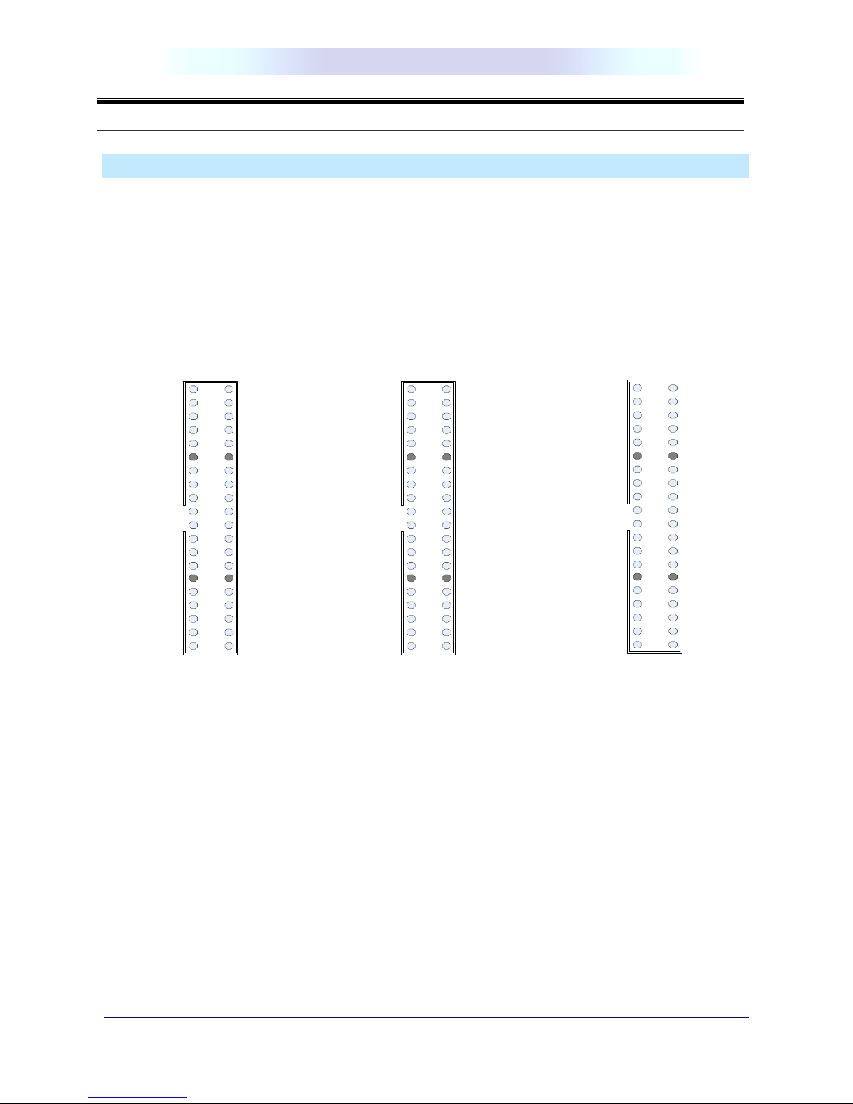
The THDB-HTG board provides users a prototyping area for signal measurement or debug. These
prototyping points are connected to the HSTC/HSMC connector directly. Detailed I/O maps for HSTC and
HSMC version are provided to help users locate the corresponding prototyping points, as shown in Figure 3.4
and Figures 3.5, respectively.
HSTC_TX_n8
HSTC_TX_p8
HSTC_RX_n8
HSTC_RX_p8
HSTC_TX_n17
HSTC_TX_p17
HSTC_RX_n17
HSTC_RX_p17
HSTC_TX_n27
HSTC_TX_p27
HSTC_RX_n28
HSTC_RX_p28
HSTC_TX_n29
HSTC_TX_p29
HSTC_CLKIN_2
HSTC_CLKOUT_2
HSTC_TX_n27
HSTC_TX_p27
HSTC_RX_n28
HSTC_RX_p28
HSTC_TX_n29
HSTC_TX_p29
Figure 3.4 Pin distribution of the prototype area for TDHB-HTG HSTC version
HSMC_TX_n8
HSMC_TX_p8
HSMC_RX_n8
HSMC_RX_p8
HSMC_D2
HSMC_D0
HSMC_D3
HSMC_D1
ND
HSMC_TXVR_TXn6
HSMC_TXVR_TXp6
ND
HSMC_TXVR_TXn7
HSMC_TXVR_TXp7
HSMC_CLKIN0
HSMC_CLKOUT0
ND
HSMC_TXVR_RXn6
HSMC_TXVR_RXp6
ND
HSMC_TXVR_RXn7
HSMC_TXVR_RXp7
ND : Not Defin ed
Figure 3.5 Pin distribution of the prototype area for TDHB-HTG HSMC version
Page 15

Board Components
13
1-8JTAG Switch
The THDB-HTG board provides a JTAG switch (SW1) to short the JTGA signal “HSTC_TDI” and
“HSTC_TDO” together. When the THDB-HTG board is connected to a HSTC host board, this feature can
bypass the JTAG signal from host board to form a close loop of JTAG chain. For example, if users connect a
THDB-HTG with Altera DE3 board, this switch must be turned on, or the Stratix III FPGA device will not be
detected because the JTGA chain is not a close loop on DE3 board. Figure 3.6 shows the JTAG switch being
turned on.
Figure 3.6 The JTAG Switch in “ON” position
1-9Power ON Control Pin
Pin 121 of the HSTC connector is defined as a “Power ON” control signal. This signal allows host board to
turn on/off the power supply on THDB-HTG board. When the Power ON signal is in logic low level, the 3.3V
and 5V on the expansion header will not supply any power. This feature is designed for THDB-HTG HSTC
version only.
1-10I2C Serial EEPROM
This section describes the I2C Serial EEPROM on the THDB-HTG board
The THDB-HTG board provides a Microchip 24LC02BT EEPROM (U1) which can be configured by the I2C
interface. The size of the EEPROM is 2K-bit that can store the board information or user’s data. The detailed
pin description between EEPROM and HSMC connector is listed in the Table 3.4.
Page 16

Board Components
14
Table 3.4 The pin assignments of the I2C serial EEPROM
EEPROM
Pin Number
EPPROM
Signal Name
HSMC Pin
Number
U1-1 A0 N/A
U1-2 A1 N/A
U1-3 A2 N/A
U1-4 GND N/A
U1-5 HSTC_SDA J1-131
U1-6 HSTC_SCL J1-132
U1-7 WP N/A
U1-8 VCC33 (3.3 volts) N/A
1-11Power Supply
This section describes the power supply on the THDB-HTG board.
The power distribution on the THDB-HTG board is shown in Figure 3.7.
EEPROM
U1
12V
J1
Regulator
Q1
5V
Expansion
Prototype
Connectors
J2~J4
3.3V
HSTC/HSMC
Connector
Figure 3.7 THDB-HTG board power distribution diagram.
Page 17

Demonstration
15
Demonstration
4
This chapter illustrates how to use the THDB-HTG board to a HSTC/HSMC-interfaced host
board.
1-12Connecting THDB-HTG Board to a Cyclone III Starter Board
This section describes how to use the THDB-HTG board with a Cyclone III Starter Board.
Figure 4.1 illustrates how the THDB-HTG board is connected to the Cyclone III starter board. Users need to
pay extra attention to the following two points:
1. Observe the orientation of the HSMC connector when connecting the THDB-HTG to the Cyclone
III Starter Board.
2. Note that there are two LVDS pairs on the HSMC connector: the HSMC_CLK_p1/n1 (form a close
loop via R3) and HSMC_CLKIN_p2/n2 (form a close loop via R4). Therefore, using any one of the
signal in a L VDS pair und er single-ended mode will prevent users fro m using the other signal in the
same pair .
Figure 4.1 Connecting the THDB-HTG board to the Cyclone III starter board
Page 18

Demonstration
16
1-13Connecting THDB-HTG Board to Altera DE3 Board
This section describes how to use the THDB-HTG board with Altera DE3 Board.
Figure 4.2 illustrates how the THDB-HTG board is connected to the Altera DE3 board. Users need to pay extra
attention to the following three points:
1. THDB-HTG board can be connected to any of the HSTC connectors J1, J3, J5, and J7 on the DE3
board.
2. The JTAG Switch on the THDB-HT G board M UST be switched to “Byp ass” posit ion, or the FPGA device
on DE3 board will not be detected.
3. Users can use DE3_System_builder to create Quartus II project. Please refer to Figure 3.2 for the
corresponding signal names.
Figure 4.2 Connecting the THDB-HTG board to the Cyclone III starter board
Page 19

Appendix
17
Appendix
5
1-14Mechanical
1-15Revision History
Date Change Log
DEC 23, 2009 Initial Version
1-16Always Visit THDB-HTG Webpage for New Main board
We will be continuing providing interesting examples and labs on our THDB-HTG
webpage. Please visit www.altera.com or HTG.terasic.com for more information.
Page 20

5
5
4
4
3
3
2
2
1
1
D D
C C
B B
A A
HSTC_TDO
HSTC_TCK
VCC5
VREF VTT
HSTC_TMS
HSTC_TDI
HSTC_RX_p1
HSTC_RX_p2
HSTC_RX_p3
HSTC_RX_p4
HSTC_RX_p5
HSTC_RX_p6
HSTC_RX_p7
HSTC_RX_p0
HSTC_RX_p8
HSTC_RX_n1
HSTC_RX_n2
HSTC_RX_n3
HSTC_RX_n4
HSTC_RX_n5
HSTC_RX_n6
HSTC_RX_n7
HSTC_RX_n8
HSTC_RX_n0
HSTC_RX_p11
HSTC_RX_p9
HSTC_RX_p10
HSTC_RX_n11
HSTC_RX_n9
HSTC_RX_n10
HSTC_RX_n12
HSTC_RX_n17
HSTC_RX_n13
HSTC_RX_n14
HSTC_RX_n15
HSTC_RX_n16
HSTC_RX_p12
HSTC_RX_p17
HSTC_RX_p13
HSTC_RX_p14
HSTC_RX_p15
HSTC_RX_p16
HSTC_RX_n23
HSTC_RX_p23
HSTC_RX_n22
HSTC_RX_p22
HSTC_RX_n21
HSTC_RX_p21
HSTC_RX_n29
HSTC_RX_n25
HSTC_RX_n28
HSTC_RX_n27
HSTC_RX_p29
HSTC_RX_p25
HSTC_RX_p27
HSTC_RX_p28
HSTC_RX_n24
HSTC_RX_p24
HSTC_RX_n20
HSTC_RX_n18
HSTC_RX_n19
HSTC_RX_p20
HSTC_RX_p19
HSTC_RX_p18
HSTC_SDA HSTC_SCL
POWER_ON
HSTC_CLKOUT_2
HSTC_CLKIN_n0
HSTC_CLKIN_p0
HSTC_CLKIN_n1
HSTC_CLKIN_p1
HSTC_CLKIN_2
HSTC_RX_p26
HSTC_RX_n26
HSTC_TX_n1
HSTC_TX_n2
HSTC_TX_n3
HSTC_TX_n4
HSTC_TX_n5
HSTC_TX_n6
HSTC_TX_n7
HSTC_TX_n0
HSTC_TX_n8
HSTC_TX_p1
HSTC_TX_p2
HSTC_TX_p3
HSTC_TX_p4
HSTC_TX_p5
HSTC_TX_p0
HSTC_TX_p6
HSTC_TX_p7
HSTC_TX_p8
HSTC_CLKOUT_n0
HSTC_CLKOUT_p0
HSTC_CLKOUT_n1
HSTC_CLKOUT_p1
HSTC_TX_n9
HSTC_TX_n10
HSTC_TX_p9
HSTC_TX_p10
HSTC_TX_n11
HSTC_TX_p11
HSTC_TX_n12
HSTC_TX_p12
HSTC_TX_n13
HSTC_TX_p13
HSTC_TX_n14
HSTC_TX_p14
HSTC_TX_n15
HSTC_TX_p15
HSTC_TX_n16
HSTC_TX_p16
HSTC_TX_n17
HSTC_TX_p17
HSTC_TX_n18
HSTC_TX_p18
HSTC_TX_n19
HSTC_TX_p19
HSTC_TX_n20
HSTC_TX_p20
HSTC_TX_n21
HSTC_TX_p21
HSTC_TX_n22
HSTC_TX_p22
HSTC_TX_n23
HSTC_TX_p23
HSTC_TX_n24
HSTC_TX_p24
HSTC_TX_n25
HSTC_TX_p25
HSTC_TX_n26
HSTC_TX_p26
HSTC_TX_n27
HSTC_TX_p27
HSTC_TX_n28
HSTC_TX_p28
HSTC_TX_n29
HSTC_TX_p29
HSTC_SDA
HSTC_SCL
POWER_ON
HSTC_CLKOUT_2
HSTC_CLKIN_2
HSTC_TMS
HSTC_TCK
HSTC_TDI HSTC_TDO
HSTC_TDO
HSTC_TDI
POWER_ON
HSTC_CLKOUT_n0
HSTC_CLKOUT_p0
HSTC_CLKIN_n0
HSTC_CLKIN_p0
HSTC_TX_n1
HSTC_TX_n2
HSTC_TX_n3
HSTC_TX_n4
HSTC_TX_n5
HSTC_TX_p1
HSTC_TX_p2
HSTC_TX_p3
HSTC_TX_p4
HSTC_TX_n6 HSTC_TX_n7
HSTC_TX_p5
HSTC_TX_p6 HSTC_TX_p7
HSTC_RX_p1
HSTC_RX_p2
HSTC_RX_p3
HSTC_RX_p4
HSTC_RX_p5
HSTC_RX_p6
HSTC_RX_p7
HSTC_RX_p0
HSTC_RX_n1
HSTC_RX_n2
HSTC_RX_n3
HSTC_RX_n4
HSTC_RX_n5
HSTC_RX_n6
HSTC_RX_n7
HSTC_RX_n0
HSTC_TX_n0
HSTC_TX_p0
HSTC_TX_n8
HSTC_TX_p8
HSTC_TX_n11
HSTC_TX_p11
HSTC_TX_n12
HSTC_TX_p12
HSTC_TX_n13
HSTC_TX_p13
HSTC_TX_n14
HSTC_TX_p14
HSTC_TX_n15
HSTC_TX_p15
HSTC_CLKOUT_n1
HSTC_CLKOUT_p1
HSTC_TX_n9
HSTC_TX_n10
HSTC_TX_p9
HSTC_TX_p10
HSTC_RX_p8
HSTC_RX_n8
HSTC_RX_p11
HSTC_RX_p9
HSTC_RX_p10
HSTC_RX_n11
HSTC_RX_n9
HSTC_RX_n10
HSTC_RX_n12
HSTC_RX_n13
HSTC_RX_n14
HSTC_RX_n15
HSTC_RX_p12
HSTC_RX_p13
HSTC_RX_p14
HSTC_RX_p15
HSTC_CLKIN_n1
HSTC_CLKIN_p1
HSTC_TX_n16
HSTC_TX_p16
HSTC_TX_n17
HSTC_TX_p17
HSTC_RX_n17
HSTC_RX_n16
HSTC_RX_p17
HSTC_RX_p16
HSTC_TX_p18
HSTC_TX_n18
HSTC_TX_n19
HSTC_TX_p19
HSTC_TX_n20
HSTC_TX_p20
HSTC_TX_n21
HSTC_TX_p21
HSTC_TX_n22
HSTC_TX_p22
HSTC_TX_n23
HSTC_TX_p23
HSTC_TX_n24
HSTC_TX_p24
HSTC_RX_n22
HSTC_RX_n21
HSTC_RX_p21
HSTC_RX_n20
HSTC_RX_n18
HSTC_RX_n19
HSTC_RX_p20
HSTC_RX_p19
HSTC_RX_p18
HSTC_RX_n23
HSTC_RX_p23
HSTC_RX_p22
HSTC_RX_n24
HSTC_RX_p24
HSTC_TX_p25
HSTC_TX_n25
HSTC_TX_n26
HSTC_TX_p26
HSTC_TX_n29
HSTC_TX_p29
HSTC_TX_n27
HSTC_TX_p27
HSTC_TX_n28
HSTC_TX_p28
HSTC_RX_n29
HSTC_RX_n28
HSTC_RX_n27
HSTC_RX_p29
HSTC_RX_p27
HSTC_RX_p28
HSTC_RX_p26
HSTC_RX_n26
HSTC_RX_n25
HSTC_RX_p25
5V
12V
VCC33
5V
5V
VCC33
5V
VCC33
3V3
3V3
3V3
3V3 12V
VCC333V3
VCC33
VCC33
12V3V3 5V
3V3
Title
Size Document Number Rev
Date: Sheet
of
Copyright (c) 2008 by Terasic Technologies Inc. Taiwan.
No part of this schematic design may be reproduced, duplicated, or used without the prior written permission of Terasic.
All rights reserved.
High Speed Terasic Connector (HSTC)
1.0
HSTC TO GPIO Daughter Board
C
11Thursday, October 30, 2008
HSTC Connector - Female (Motherboard Bottom-side)
or Daughter Board
Attention:
2. If the JTAG signals are not used on the daughter board,
please short TDI with TDO (see Example 2).
5. Pin 2 must be connected to GND to enable the auto JTAG chain detection.
3. The voltage level of VTT and VREF is half the I/O voltage of
the HSTC connector.
4. Daughter board should supply power to VTT and VREF.
1. Both JTAG and I2C signals are fixed at 3.3V.
Short
TDO (125)
TMS (130)
TCK (129)
HSTC Daughter Board
Daughter Board Circuit
Part Number : QSH-090-01-F-D-A
HSTC Female
TDI (126)
Example 2:
Attention: R14 HSMC only
R12KR1
2K
R11
240
R11
240
TXn27TXn27
FID6FID6
TDITDI
RXn17RXn17
R14 0 NMR14 0 NM
FID7FID7
RXn29RXn29
TXp27TXp27
BC5
0.1u
BC5
0.1u
TDOTDO
RXp17RXp17
3V33V3
FID8FID8
MH3MH3
A1
A0
VSS
A2
VCC
SDA
SCL
WP
U1
24LC02B
A1
A0
VSS
A2
VCC
SDA
SCL
WP
U1
24LC02B
4 5
6
8
7
1
2
3
9
TXn28TXn28
FID1FID1
BC6
0.1u
BC6
0.1u
VCC5VCC5
Q1A
SI5519DU
Q1A
SI5519DU
TXp28TXp28
FID2FID2
J2
BOX HEADER 2X20
J2
BOX HEADER 2X20
1 2
3 4
5 6
7 8
9 10
111312
14
16
18
20
22
24
26
27
15
17
19
21
23
25
28
29
31
33
35
37
39
30
32
34
36
38
40
C6
100uC6100u
TMSTMS
BC7
0.1u
BC7
0.1u
R12 10KR12 10K
TXn29TXn29
FID3FID3
12V12V
TCKTCK
C4
100uC4100u
FID4FID4
TXp29TXp29
Q1BQ1B
J4
BOX HEADER 2X20
J4
BOX HEADER 2X20
1 2
3 4
5 6
7 8
9 10
111312
14
16
18
20
22
24
26
27
15
17
19
21
23
25
28
29
31
33
35
37
39
30
32
34
36
38
40
R13
120
R13
120
5V5V
MH1MH1
TXn8TXn8
C8
100uC8100u
C3 1nC3 1n
181182183184188 185186187189192 190191
J1
QSH-090-01-F-D-A
181182183184188 185186187189192 190191
J1
QSH-090-01-F-D-A
1
1
3
3
5
5
7
7
9
9
11
11
13
13
15
15
17
17
19
19
21
21
23
23
25
25
27
27
29
29
31
31
33
33
35
35
37
37
39
39
41
41
43
43
45
45
47
47
49
49
51
51
53
53
55
55
57
57
59
59
2
2
4
4
6
6
8
8
10
10
12
12
14
14
16
16
18
18
20
20
22
22
24
24
26
26
28
28
30
30
32
32
34
34
36
36
38
38
40
40
42
42
44
44
46
46
48
48
50
50
52
52
54
54
56
56
58
58
60
60
61
61
63
63
65
65
67
67
69
69
71
71
73
73
75
75
77
77
79
79
81
81
83
83
85
85
87
87
89
89
91
91
93
93
95
95
97
97
99
99
101
101
103
103
105
105
107
107
109
109
111
111
113
113
115
115
117
117
119
119
62
62
64
64
66
66
68
68
70
70
72
72
74
74
76
76
78
78
80
80
82
82
84
84
86
86
88
88
90
90
92
92
94
94
96
96
98
98
100
100
102
102
104
104
106
106
108
108
110
110
112
112
114
114
116
116
118
118
120
120
121
121
123
123
125
125
127
127
129
129
131
131
133
133
135
135
137
137
139
139
141
141
143
143
145
145
147
147
149
149
151
151
153
153
155
155
157
157
159
159
161
161
163
163
165
165
167
167
169
169
171
171
173
173
175
175
177
177
179
179
122
122
124
124
126
126
128
128
130
130
132
132
134
134
136
136
138
138
140
140
142
142
144
144
146
146
148
148
150
150
152
152
154
154
156
156
158
158
160
160
162
162
164
164
166
166
168
168
170
170
172
172
174
174
176
176
178
178
180
180
181
181
182
182
183
183
184
184
185
185
186
186
187
187
188
188
189
189
190
190
191
191
192
192
C1
10uC110u
POWER
LEDB
POWER
LEDB
TXp8TXp8
MH2MH2
R7 0 NMR7 0 NM
1
ON
SW1
SW-Button
1
ON
SW1
SW-Button
1 2
C51nC5
1n
R5 0 NMR5 0 NM
R22KR2
2K
MH4MH4
VREFVREF
RXn27RXn27
BC1
0.1u
BC1
0.1u
R9 6.2KR9 6.2K
CLKOUT2CLKOUT2
R3 0 NMR3 0 NM
RXn28RXn28
U2 LT1963AES8U2 LT1963AES8
IN
8
GND
3
OUT
1
GND
7
SHDN
5
GND
6
SENSE
2
CLKIN2CLKIN2
RXp27RXp27
R4 0R4 0
BC2
0.1u
BC2
0.1u
TXn17TXn17
C7
100uC7100u
RXp29RXp29
J3
BOX HEADER 2X20
J3
BOX HEADER 2X20
1 2
3 4
5 6
7 8
9 10
111312
14
16
18
20
22
24
26
27
15
17
19
21
23
25
28
29
31
33
35
37
39
30
32
34
36
38
40
R6 0R6 0
BC3
0.1u
BC3
0.1u
TXp17TXp17
C2
10uC210u
RXp28RXp28
VTTVTT
RXn8RXn8
R8 0R8 0
BC4
0.1u
BC4
0.1u
R10
1.96K
R10
1.96K
FID5FID5
RXp8RXp8
 Loading...