

Terasic THDB-H2G
THDB-H2G
Terasic HSMC to GPIO Daughter Board
User Manual
Document Version 1.0 AUG. 15, 2007 by Terasic

Introduction
Page Index
CHAPTER 1 INTRODUCTION...................................................................................................................................1
1-1 FEATURES................................................................................................................................................................1
1-2 GETTING HELP ........................................................................................................................................................1
CHAPTER 2 ARCHITECTURE..................................................................................................................................2
2-1 LAY OUT AND COMPONETS.......................................................................................................................................2
2-2 BLOCK DIAGRAM .....................................................................................................................................................4
CHAPTER 3 BOARD COMPONENTS.....................................................................................................................5
3-1 HSMC EXPANSION CONNECTOR.............................................................................................................................5
3-2 EXPANSION PROTOTYPE CONNECTORS..................................................................................................................8
3-3 I2C SERIAL EEPROM..........................................................................................................................................13
3-4 POWER SUPPLY.....................................................................................................................................................13
CHAPTER 4 DEMONSTRATION............................................................................................................................14
4-1 CONNECTING THDB-H2G BOARD TO CYCLONE III STARTER BOARD ................................................................14
CHAPTER 5 APPENDIX...........................................................................................................................................15
5-1 REVISION HISTORY................................................................................................................................................15
5-2 ALWAYS VISIT THDB-H2G WEBPAGE FOR NEW MAIN BOARD............................................................................15
ii
Introduction
1
The THDB-H2G board is designed to fan out the High Speed Mezzanine connector (HSMC) I/Os to three
40-pin expansion prototype connectors, which are compatible with Altera DE2/DE1 expansion headers. Users
can connect up to three Altera DE2/DE1 boards (or associated daughter cards) onto a HSMC-interfaced host
board via the THDB-H2G board.
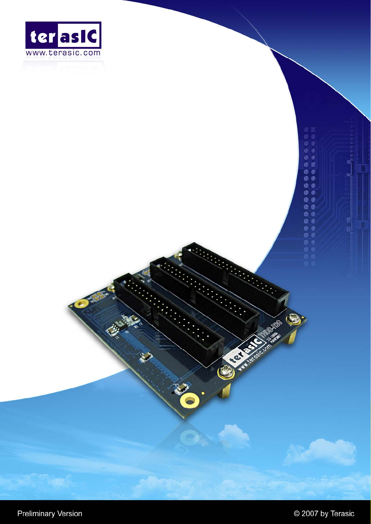
Figure 1.1 shows the photo of the THDB-H2G board. The important functions of the THDB-H2G are listed
below:
Converts HSMC interface I/O to standard 40-pi n expansion connectors.
•
• Allows users to connect Altera DE2/DE1 board
• Provides test points for signal measurement.
Introduction
1-1Features
to a HSMC-interfaced host board.
s
Figure 1.1. The picture of the THDB-H2G
1-2Getting Help
Here are some places to get help if you encounter any problem:
9 Email to support@terasic.com
Taiwan & China: +886-3-550-8800
9
Korea : +82-2-512-7661
9
9 Japan: +81-428-77-7000
1
board
Architecture
2
This chapter describes the architecture of the THDB-H2G board including block diagram and components.
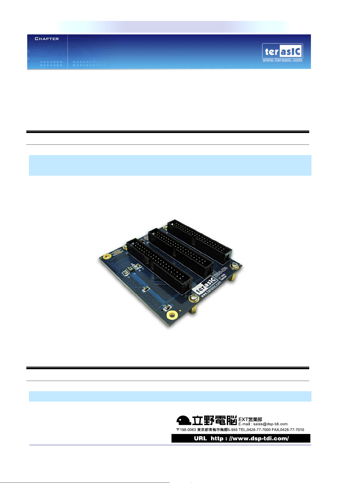
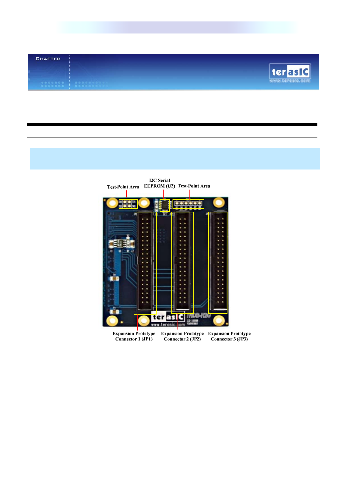
The picture of the TDRB-H2G is shown in Figure 2.1 and Figure 2.2. It depicts the layout of the board and
indicates the locations of the connectors and key components.
Architecture
1-3Layout and Componets
Figure 2.1 The TDRB-H2G board PCB and component diagram
2
HSM
Architecture
C Connector(J1)
Figure 2.2 The TDRB-H2G board back side – HSMC connector view
The following components are provided on the THDB-H2G board :
• HSMC expansion connector (J1)
• Expansion prototype connectors (JP1,JP2,JP3)
• I2C serial EEPROM (U2)
3
Architecture
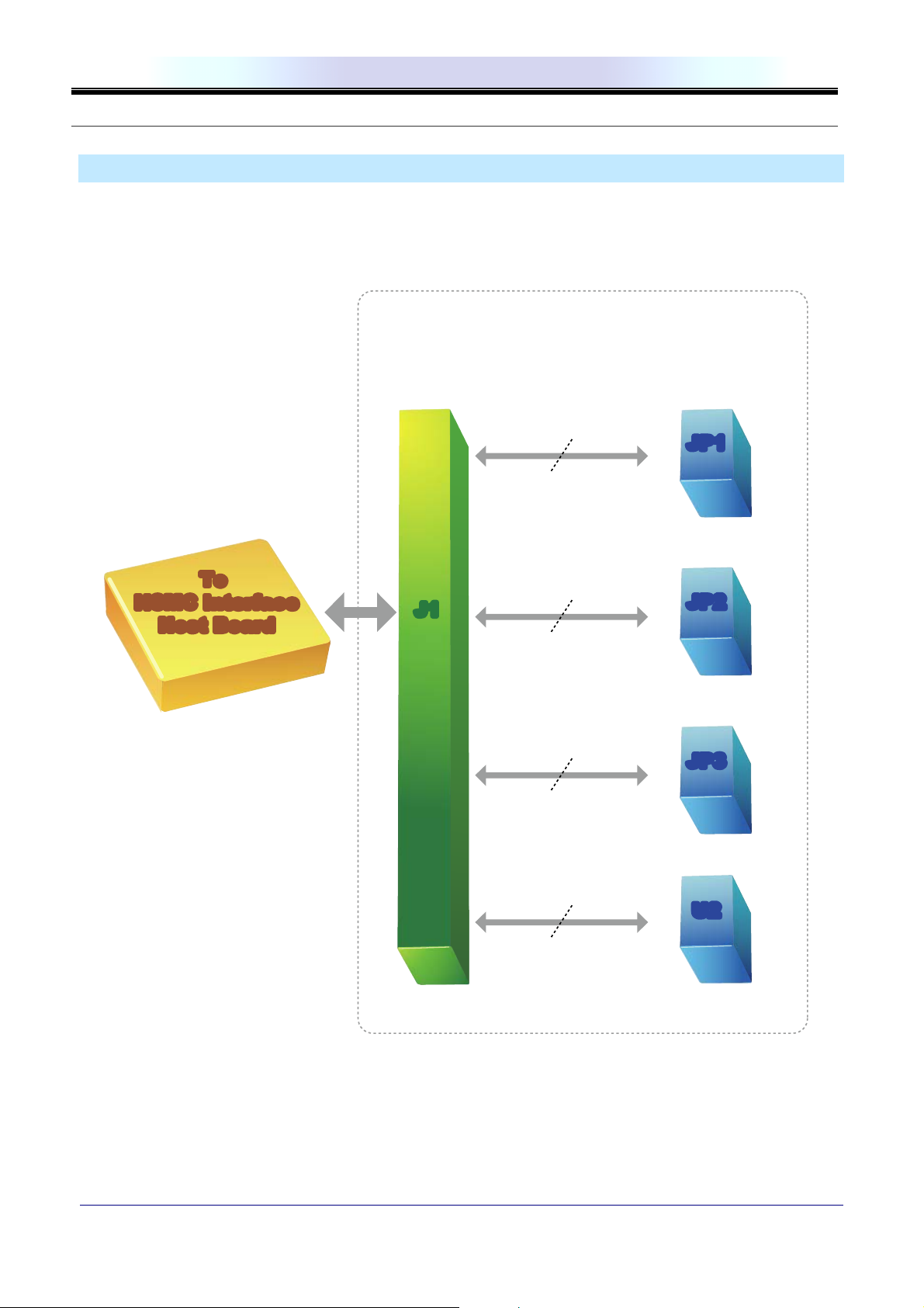
1-4Block Diagram
Figure 2.3 shows the block diagram of the THDB-H2G board.
THDB-H2G
To
HSMC Interface
Host Board
HSMC
Connector
J1
40-Pin Expansion
Prototype Connector 1
36 I/Os
JP1
40-Pin Expansion
Prototype Connector 2
36 I/Os
JP2
40-Pin Expansion
Prototype Connector 3
36 I/Os
JP3
I2C Serial EEPROM
I2C Interface
U2
Figure 2.3. The block diagram of the THDB-H2G board
4

Board Components
3
Board Components
This section will describe the detailed information of the components, connector interfaces,
and the pin mappings on the THDB-H2G board.
1-5HSMC Expansion Connector
This section describes the HSMC connector on the THDB-H2G board
THDB-H2G board contains an Altera standard HSMC connector. All the other interfaces on the THDB-H2G
board are connected to the HSMC connector. Figure 3.1, Figure 3.2, and Figure 3.3 show the pin-outs of the
HSMC connector.
10
12
14
16
18
20
22
24
26
28
30
32
34
36
38
40
2
4
6
8
1
HSMC_TXVR_TXp7
3
HSMC_TXVR_TXn7
5
HSMC_TXVR_TXp6
7
HSMC_TXVR_TXn6
9
HSMC_TXVR_TXp5
11
HSMC_TXVR_TXn5
13
HSMC_TXVR_TXp4
15
HSMC_TXVR_TXn4
17
HSMC_TXVR_TXp3
19
HSMC_TXVR_TXn3
21
HSMC_TXVR_TXp2
23
HSMC_TXVR_TXn2
25
HSMC_TXVR_TXp1
27
HSMC_TXVR_TXn1
29
HSMC_TXVR_TXp0
31
HSMC_TXVR_TXn0
33
HSMC_SDA
35
HSMC_TCK
37
HSMC_TDO
39
HSMC_CLKOUT0
HSMC_TXVR_RXp7
HSMC_TXVR_RXn7
HSMC_TXVR_RXp6
HSMC_TXVR_RXn6
HSMC_TXVR_RXp5
HSMC_TXVR_RXn5
HSMC_TXVR_RXp4
HSMC_TXVR_RXn4
HSMC_TXVR_RXp3
HSMC_TXVR_RXn3
HSMC_TXVR_RXp2
HSMC_TXVR_RXn2
HSMC_TXVR_RXp1
HSMC_TXVR_RXn1
HSMC_TXVR_RXp0
HSMC_TXVR_RXn0
HSMC_SCL
HSMC_TMS
HSMC_TDI
HSMC_CLKIN0
Figure 3.1 The pin-outs of Bank 1 on the HSMC connector.
5

Board Components
HSMC_D1
HSMC_D3
12V
HSMC_RX_p0
HSMC_RX_n0
12V
HSMC_RX_p1
HSMC_RX_n1
12V
HSMC_RX_p2
HSMC_RX_n2
12V
HSMC_RX_p3
HSMC_RX_n3
12V
HSMC_RX_p4
HSMC_RX_n4
12V
HSMC_RX_p5
HSMC_RX_n5
12V
HSMC_RX_p6
HSMC_RX_n6
12V
HSMC_RX_p7
HSMC_RX_n7
12V
HSMC_CLKINp1
HSMC_CLKINn1
12V
42
44
46
48
50
52
54
56
58
60
62
64
66
68
70
72
74
76
78
80
82
84
86
88
90
92
94
96
98
100
HSMC_D0
41
HSMC_D2
43
VCC33
45
HSMC_TX_p0
47
HSMC_TX_n0
49
VCC33
51
HSMC_TX_p1
53
HSMC_TX_n1
55
VCC33
57
HSMC_TX_p2
59
HSMC_TX_n2
61
VCC33
63
HSMC_TX_p3
65
HSMC_TX_n3
67
VCC33
69
HSMC_TX_p4
71
HSMC_TX_n4
73
VCC33
75
HSMC_TX_p5
77
HSMC_TX_n5
79
VCC33
81
HSMC_TX_p6
83
HSMC_TX_n6
85
VCC33
87
HSMC_TX_p7
89
HSMC_TX_n7
91
VCC33
93
HSMC_CLKOUTp1
95
HSMC_CLKOUTn1
97
VCC33
99
Figure 3.2 The pin-outs of Bank 2 on the HSMC connector
6

HSMC_RX_p8
HSMC_RX_n8
12V
HSMC_RX_p9
HSMC_RX_n9
12V
HSMC_RX_p10
HSMC_RX_n10
12V
HSMC_RX_p11
HSMC_RX_n11
12V
HSMC_RX_p12
HSMC_RX_n12
12V
HSMC_RX_p13
HSMC_RX_n13
12V
HSMC_RX_p14
HSMC_RX_n14
12V
HSMC_RX_p15
HSMC_RX_n15
12V
HSMC_RX_p16
HSMC_RX_n16
12V
HSMC_CLKINp2
HSMC_CLKINn2
GND
102
104
106
108
110
112
114
116
118
120
122
124
126
128
130
132
134
136
138
140
142
144
146
148
150
152
154
156
158
160
Board Components
101
HSMC_TX_p8
103
HSMC_TX_n8
105
VCC33
107
HSMC_TX_p9
109
HSMC_TX_n9
111
VCC33
113
HSMC_TX_p10
115
HSMC_TX_n10
117
VCC33
119
HSMC_TX_p11
121
HSMC_TX_n11
123
VCC33
125
HSMC_TX_p12
127
HSMC_TX_n12
129
VCC33
131
HSMC_TX_p13
133
HSMC_TX_n13
135
VCC33
137
HSMC_TX_p14
139
HSMC_TX_n14
141
VCC33
143
HSMC_TX_p15
145
HSMC_TX_n15
147
VCC33
149
HSMC_TX_p16
151
HSMC_TX_n16
153
VCC33
155
HSMC_CLKOUTp2
157
HSMC_CLKOUTn2
159
VCC33
Figure 3.3 The pin-outs of Bank 3 on the HSMC connector.
7

Board Components
1-6Expansion Prototype Connectors
This section describes the expansion prototype connectors on the THDB -H2G board.
The THDB-H2G board has three expansion prototype connectors (JP1, JP2, and JP3) connected to the
HSMC connector directly. Each of the connectors has 36 prototyping I/Os and 3.3/5 volts power supply from
the HSMC interface and on-board regulator. In addition, the expansion connector is compatible with the
expansion headers of the Altera DE1/DE2 board. With these expansion connectors, users can connect the
Altera DE2/DE1 development kits or custom daughter boards to a HSMC-interfaced host board. Figure 3.4,
Figure 3.5, and Figure 3.6 shows the pin-outs of the expansion prototype connectors. Also, the detailed pin
mappings to HSMC connector are listed in Table 3.1, Table3.2, and Table 3.3.
Figure 3.4 The pin-outs of the expa nsion prototype connector JP1
8

Board Components
Figure 3.5 The pin-outs of the expa nsion prototype connector JP2
Figure 3.6 The pin-outs of the expa nsion prototype connector JP3
9

r
Board Components
Table 3.1 The pin mappings of the expansion prototype connector JP1
Expansion Prototype Connector 1 - JP1
Pin Numbe
1 HSMC_CLKIN0 40 GPIO0
2 HSMC_TXVR_TXp6 5 GPIO1
3 HSMC_TXVR_TXp5 9 GPIO2
4 HSMC_TXVR_TXn6 7 GPIO3
5 HSMC_TXVR_TXn5 11 GPIO4
6 HSMC_TXVR_TXp4 13 GPIO5
7 HSMC_TXVR_TXp3 17 GPIO6
8 HSMC_TXVR_TXn4 15 GPIO7
9 HSMC_TXVR_TXn3 19 GPIO8
10 HSMC_TXVR_TXp2 21 GPIO9
11 5V N/A N/A
12 GND N/A N/A
13 HSMC_TXVR_TXn2 23 GPIO10
14 HSMC_TXVR_TXp1 25 GPIO11
15 HSMC_TXVR_TXp0 29 GPIO12
16 HSMC_TXVR_TXn1 27 GPIO13
17 HSMC_TXVR_TXn0 31 GPIO14
18 HSMC_TXVR_RXp5 10 GPIO15
19 HSMC_CLKOUT0 39 GPIO16
20 HSMC_TXVR_RXn5 12 GPIO17
21 HSMC_TXVR_RXp4 14 GPIO18
22 HSMC_TXVR_RXn4 16 GPIO19
23 HSMC_TXVR_RXp3 18 GPIO20
24 HSMC_TXVR_RXn3 20 GPIO21
25 HSMC_TXVR_RXp2 22 GPIO22
26 HSMC_TXVR_RXn2 24 GPIO23
27 HSMC_TXVR_RXp1 26 GPIO24
28 HSMC_TXVR_RXn1 28 GPIO25
29 VCC33 (3.3 volts) N/A N/A
30 GND N/A N/A
31 HSMC_TXVR_RXn0 32 GPIO26
32 HSMC_TXVR_RXp0 30 GPIO27
33 HSMC_TX_p7 89 GPIO28
34 HSMC_TX_n7 91 GPIO29
35 HSMC_RX_n5 80 GPIO30
36 HSMC_RX_p5 78 GPIO31
37 HSMC_TX_p8 101 GPIO32
38 HSMC_TX_n8 103 GPIO33
39 HSMC_RX_p8 102 GPIO34
40 HSMC_RX_n8 104 GPIO35
Signal Name HSMC Pin DE2/DE1
10

r
Board Components
Table 3.2 The pin mappings of the expansion prototype connector JP2
Expansion Prototype Connector 2 –JP2
Pin Numbe
1 HSMC_CLKINp1 96 GPIO0
2 HSMC_D2 43 GPIO1
3 HSMC_CLKINn1 98 GPIO2
4 HSMC_D0 41 GPIO3
5 HSMC_TX_p0 47 GPIO4
6 HSMC_TX_p1 53 GPIO5
7 HSMC_TX_n0 49 GPIO6
8 HSMC_TX_n1 55 GPIO7
9 HSMC_TX_p2 59 GPIO8
10 HSMC_TX_n2 61 GPIO9
11 5V N/A N/A
12 GND N/A N/A
13 HSMC_TX_n3 67 GPIO10
14 HSMC_TX_p3 65 GPIO11
15 HSMC_TX_n4 73 GPIO12
16 HSMC_TX_p4 71 GPIO13
17 HSMC_TX_n5 79 GPIO14
18 HSMC_TX_p5 77 GPIO15
19 HSMC_CLKOUTp1 95 GPIO16
20 HSMC_TX_p6 83 GPIO17
21 HSMC_CLKOUTn1 97 GPIO18
22 HSMC_TX_n6 85 GPIO19
23 HSMC_D1 42 GPIO20
24 HSMC_D3 44 GPIO21
25 HSMC_RX_p0 48 GPIO22
26 HSMC_RX_p1 54 GPIO23
27 HSMC_RX_n0 50 GPIO24
28 HSMC_RX_n1 56 GPIO25
29 VCC33 (3.3 volts) N/A N/A
30 GND N/A N/A
31 HSMC_RX_p2 60 GPIO26
32 HSMC_RX_n2 62 GPIO27
33 HSMC_RX_p3 66 GPIO28
34 HSMC_RX_p4 72 GPIO29
35 HSMC_RX_n3 68 GPIO30
36 HSMC_RX_n4 74 GPIO31
37 HSMC_RX_p6 84 GPIO32
38 HSMC_RX_p7 90 GPIO33
39 HSMC_RX_n6 86 GPIO34
40 HSMC_RX_n7 92 GPIO35
Signal Name HSMC Pin DE2/DE1
11

rSig
Board Components
Table 3.3 The pin mappings of the expansion prototype connector JP3
Expansion Prototype Connector 3 –JP3
Pin Numbe
1 HSMC_CLKINp2 156 GPIO0
2 HSMC_TX_p9 107 GPIO1
3 HSMC_CLKINn2 158 GPIO2
4 HSMC_TX_n9 109 GPIO3
5 HSMC_TX_p10 113 GPIO4
6 HSMC_TX_p11 119 GPIO5
7 HSMC_TX_n10 115 GPIO6
8 HSMC_TX_n11 121 GPIO7
9 HSMC_TX_p12 125 GPIO8
10 HSMC_TX_n12 127 GPIO9
11 5V N/A N/A
12 GND N/A N/A
13 HSMC_TX_p13 131 GPIO10
14 HSMC_TX_p14 137 GPIO11
15 HSMC_TX_n13 133 GPIO12
16 HSMC_TX_n14 139 GPIO13
17 HSMC_TX_p15 143 GPIO14
18 HSMC_TX_n15 145 GPIO15
19 HSMC_CLKOUTp2 155 GPIO16
20 HSMC_TX_p16 149 GPIO17
21 HSMC_CLKOUTn2 157 GPIO18
22 HSMC_TX_n16 151 GPIO19
23 HSMC_RX_p9 108 GPIO20
24 HSMC_RX_n9 110 GPIO21
25 HSMC_RX_p10 114 GPIO22
26 HSMC_RX_p11 120 GPIO23
27 HSMC_RX_n10 116 GPIO24
28 HSMC_RX_n11 122 GPIO25
29 VCC33 (3.3 volts) N/A N/A
30 GND N/A N/A
31 HSMC_RX_p12 126 GPIO26
32 HSMC_RX_n12 128 GPIO27
33 HSMC_RX_p13 132 GPIO28
34 HSMC_RX_p14 138 GPIO29
35 HSMC_RX_n13 134 GPIO30
36 HSMC_RX_n14 140 GPIO31
37 HSMC_RX_p15 144 GPIO32
38 HSMC_RX_p16 150 GPIO33
39 HSMC_RX_n15 146 GPIO34
40 HSMC_RX_n16 152 GPIO35
nal Name HSMC Pin DE2/DE1
12

Board Components
1-7I2C Serial EEPROM
This section describes the I2C Serial EEPROM on the THDB-H2G board
The THDB-H2G board provides a Microchip 24LC000 EEPROM (U2) which can be configured by the I2C
interface. The size of the EEPROM is 128-bit that can store the board information or user’s data. The detailed
pin description between EEPROM and HSMC connector is listed in the Table 3.4.
Table 3.4 The pin assignments of the I2C serial EEPROM
EEPROM
Pin Number
U2-1 NC N/A
U2-2 NC N/A
U2-3 NC N/A
U2-4 GND N/A
U2-5 HSMC_SDA J1-33
U2-6 HSMC_SCL J1-34
U2-7 NC N/A
U2-8 VCC33 (3.3 volts) N/A
EPPROM
Signal Name
1-8Power Supply
This section describes the power supply on the THDB-H2G board.
The power distribution on the THDB-H2G board is shown in Figure 3.7.
HSMC Pin
Number
Figure 3.7 THDB-H2G board power distribution diagram.
13

Demonstration
4
This chapter illustrates how to use the THDB-H2G board to a HSMC-interfaced host board.
1-9Connecting THDB-H2G Board to a Cyclone III Starter Board
This section describes how to use the THDB-H2G board with a Cyclone III Starter Board.
Figure 4.1 illustrates how the THDB-H2G board is connected to the Cyclone III starter board. Users need to
pay extra attention to the following two points:
1. Observe the orientation of the HSMC connector when conne cting the THDB-H2G to the Cyclone III
2. Note that there are two LVDS pairs on the HSMC connector: the HSMC_CLK_p1/n1 (form a close
Demonstration
Starter Board.
loop via R3) and HSMC_CLKIN_p2/n2 (form a close loop via R4). Therefore, using any one of the
signal in a L VDS pair und er single-ended mode will prev ent users from using the other signal in the
same pair .
Figure 4.1 Connecting the THDB-H2G board to the Cyclone III starter board
14

Appendix
5
Date Change Log
AUG 15, 2007 Initial Version
1-11Always Visit THDB-H2G Webpage for New Main board
We will be continuing providing interesting examples and labs on our THDB-H2G
webpage. Please visit www.
Appendix
1-10Revision History
terasic.com for more information.
15
 Loading...