


DE10-Pro
User Manual
1
www.terasic.com
September 24,
2019
1.1. Q

DE10-Pro
User Manual
2
www.terasic.com
September 24,
2019
Contents
Chapter 1 Overview .................................................................................. 6
1.1 General Description .............................................................................. 6
1.2 Key Features ......................................................................................... 7
1.3. Block Diagram ....................................................................................... 8
1.4. Board Power On .................................................................................. 10
Chapter 2 Board Component ................................................................ 12
2.1 Board Overview ................................................................................... 12
2.2 Configuration, Status and Setup ......................................................... 13
2.3 General User Input/Output .................................................................. 17
2.4 Temperature Sensor and Fan Control ................................................. 19
2.5 Power Monitor ..................................................................................... 21
2.6 Clock Circuit ........................................................................................ 22
2.7 FLASH Memory ................................................................................... 25
2.8 DDR4 SO-DIMM ................................................................................. 27
2.9 QSPF28 Ports ..................................................................................... 51
2.10 PCI Express ........................................................................................ 58
Chapter 3 System Builder ...................................................................... 66

DE10-Pro
User Manual
3
www.terasic.com
September 24,
2019
3.1 Introduction ......................................................................................... 66
3.2 General Design Flow ........................................................................... 67
3.3 Using System Builder .......................................................................... 68
Chapter 4 CFI-Flash Programming ....................................................... 77
4.1 FPGA Configure Operation ................................................................. 77
4.2 CFI Flash Memory Map ....................................................................... 78
4.3 Flash Example Designs ...................................................................... 79
4.4 Flash_Programming Example ............................................................. 81
4.5 Flash_Factory Example ...................................................................... 81
4.6 Flash_User Example ........................................................................... 83
4.7 Flash_Tool Example ............................................................................ 83
4.8 Programming Batch File ...................................................................... 84
4.9 Restore Factory Settings ..................................................................... 85
Chapter 5 Peripheral Reference Design ............................................... 87
5.1 Configure Si5340A in RTL ................................ ................................ ... 87
5.2 Nios II control for SI5340/ Temperature/ Power/Fan ........................... 94
5.3 Fan Speed Control ............................................................................ 101
Chapter 6 Memory Reference Design ................................................. 105
6.1 DDR4 SDRAM Test ........................................................................... 105

DE10-Pro
User Manual
4
www.terasic.com
September 24,
2019
6.2 DDR4 SDRAM Test by Nios II ........................................................... 107
6.3 QDRII+ SRAM Test ........................................................................... 112
Chapter 7 PCI Express Reference Design for Windows ................... 116
7.1 PCI Express System Infrastructure ................................................... 116
7.2 PC PCI Express Software SDK ......................................................... 117
7.3 PCI Express Software Stack ............................................................. 118
7.4 PCI Express Library API .................................................................... 123
7.5 PCIe Reference Design -Fundamental ............................................. 128
7.6 PCIe Reference Design - DDR4 ........................................................ 136
Chapter 8 PCI Express Reference Design for Linux ......................... 144
8.1 PCI Express System Infrastructure ................................................... 144
8.2 PC PCI Express Software SDK ......................................................... 145
8.3 PCI Express Software Stack ............................................................. 146
8.4 PCI Express Library API .................................................................... 148
8.5 PCIe Reference Design -Fundamental ............................................. 148
8.6 PCIe Reference Design - DDR4 ........................................................ 155
Chapter 9 Transceiver Verification ..................................................... 163
9.1 Transceiver Test Code ...................................................................... 163
9.2 Loopback Fixture ............................................................................... 163

DE10-Pro
User Manual
5
www.terasic.com
September 24,
2019
9.3 Testing by Transceiver Test Code ..................................................... 164
9.4 100G Ethernet Example (H-Tile FPGA) ............................................ 167
9.5 40G Ethernet Example (L-Tile FPGA) ............................................... 171
Chapter 10 Additional Information .................................................... 175
10.1 Getting Help ...................................................................................... 175

DE10-Pro
User Manual
6
www.terasic.com
September 24,
2019
Chapter 1
Overview
his chapter provides an overview of the DE10-Pro Development Board and
installation guide.
1.1 General Description
The Terasic DE10-Pro Stratix® 10 GX/SX FPGA Development Kit provides the ideal
hardware solution for designs that demand high capacity and bandwidth memory
interfacing, ultra-low latency communication, and power efficiency. With a full-height,
3/4-length form-factor package, the DE10-Pro is designed for the most demanding
high-end applications, empowered with the top-of-the-line Intel Stratix® 10 GX/SX,
delivering the best system-level integration and flexibility in the industry.
The Stratix® 10 GX/SX FPGA features integrated transceivers that transfer at a
maximum of 28.3 Gbps, allowing the DE10-Pro to be fully compliant with version 3.0
of the PCI Express standard, as well as allowing an ultra low-latency, straight
connections to four external 100G QSFP28 modules. Not relying on an external PHY
will accelerate mainstream development of network applications enabling customers
to deploy designs for a broad range of high-speed connectivity applications. For
designs that demand high capacity and high speed for memory and storage, the
DE10-Pro delivers with high-speed parallel flash memory and four SO-DIMM sockets
that support DDR4 SDRAM, QDR-IV and QDRII+ options to provide flexible memory
configuration. The feature-set of the DE10-Pro fully supports all high-intensity
applications such as low-latency trading, cloud computing, high-performance
computing, data acquisition, network processing, and signal processing.
T

DE10-Pro
User Manual
7
www.terasic.com
September 24,
2019
1.2 Key Features
The following hardware is implemented on the DE10-Pro board:
◼ FPGA
⚫ Intel Stratix ® 10 FPGA: 1SG280HU1F50E1VG
◼ FPGA Configuration
⚫ On-Board USB Blaster II or JTAG header for FPGA programming
⚫ Avalon-ST x8 configuration via MAX V CPLD and flash memory
⚫ AS x4 configuration via EPCQ-L configuration device (DNI)
◼ General user input/output
⚫ 4 LEDs
⚫ 2 push-buttons
⚫ 2 dip switches
◼ Clock System
⚫ 50MHz and 100MHz Oscillators
⚫ Programmable clock generators Si5340A
⚫ Two UFL connectors for external clock inputs
⚫ One 2x5 GPIO timing expansion header
◼ Memory
⚫ Four SO-DIMM Sockets, support DDR4 SDRAM, QDR-IV and QDRII+
memory modules
⚫ 128M Parallel FLASH
◼ Communication Ports
⚫ Four QSFP28 connectors
⚫ PCI Express (PCIe) x16 edge connector
◼ System Monitor and Control
⚫ Temperature sensor
⚫ Fan control

DE10-Pro
User Manual
8
www.terasic.com
September 24,
2019
⚫ Power monitor
◼ Power
⚫ One PCI Express 8-pin power connector, 12V DC Input
⚫ PCI Express edge connector power
◼ Mechanical Specification
⚫ PCI Express full-height and 3/4-length
1.3. Block Diagram
Figure 1-1 shows the block diagram of the DE10-Pro board. To provide maximum
flexibility for the users, all key components are connected to the Stratix ®10 GX/SX
FPGA device. Thus, users can configure the FPGA to implement any system design.
Figure 1-1 Block diagram of the DE10-Pro board
Below is more detailed information regarding the blocks in Figure 1-1.
◼ Stratix 10 GX/SX FPGA
⚫ GX/SX 2800
◼ 2,800K logic elements (LEs)
◼ 229 Mbits embedded memory(M20K)

DE10-Pro
User Manual
9
www.terasic.com
September 24,
2019
◼ 96 transceivers (up to 28.3Gbps)
◼ 11,520 18-bit x 19-bit multipliers
◼ 5,760 Variable-precision DSP blocks
◼ 4 PCI Express hard IP blocks
◼ 704 user I/Os
◼ 576 LVDS channels
◼ 56 phase locked loops (PLLs)
◼ JTAG Header and FPGA Configuration
⚫ On-board USB Blaster II or JTAG header for use with the Quartus
Prime Programmer
⚫ MAX V CPLD 5M2210 System Controller and Avalon-ST x8
configuration
⚫ AS x4 configuration via EPCQ-L configuration device (DNI)
◼ Memory devices
⚫ 4 SO-DIMM sockets, each supports up to 8GB ECC DDR4 SDRAM
or 16MB QDR-IV SRAM or 16MB QDRII+ SRAM
⚫ 128MB FLASH
◼ General user I/O
⚫ 4 user controllable LEDs
⚫ 2 user push buttons
⚫ 2 user dip switches
⚫ One 2x5 GPIO timing expansion header
◼ On-Board Clock
⚫ 50MHz and 100MHz Oscillators
⚫ Programming PLL providing clock for 40G/100G QSFP28 transceiver
⚫ Programming PLL providing clocks for DDR4 SDRAM, QDR-IV SRAM
and QDRII+ SRAM
DE10-Pro
User Manual
10
www.terasic.com
September 24,
2019
◼ Four QSFP28 ports
⚫ Four QSFP28 connector (40/100 Gbps+)
◼ PCI Express x16 edge connector
⚫ Support for PCIe x16 Gen1/2/3
⚫ Edge connector for PC motherboard with x16 PCI Express slot
◼ Power Source
⚫ PCI Express 8-pin DC 12V power
⚫ PCI Express edge connector power
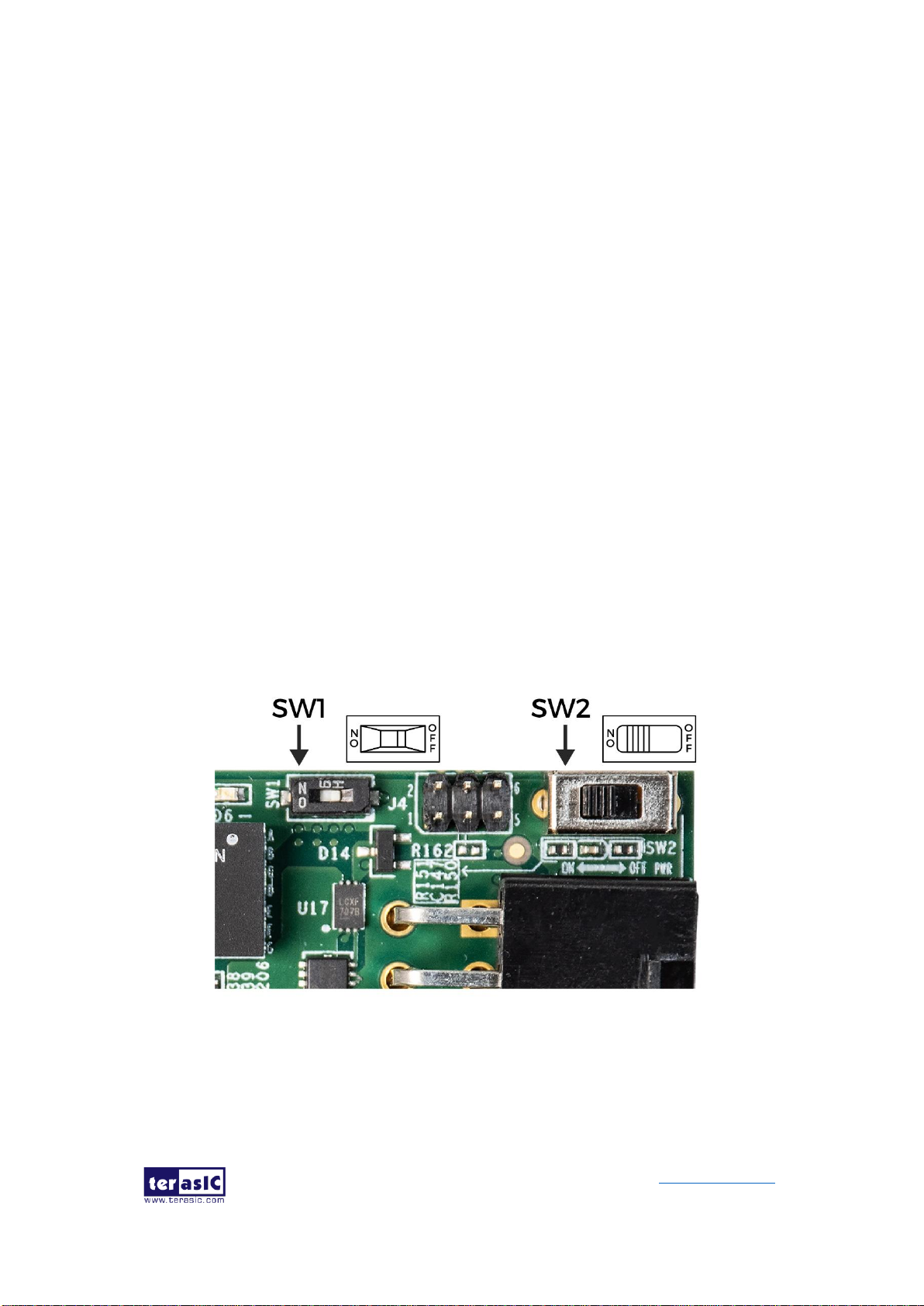
1.4. Board Power On
There are two switches SW1 and SW2 on the board which can control the board power
supply status, as shown in Figure 1-2.
Figure 1-2 Board Power Control Switches
The SW1 is default set as ON. When install the board on the PC, users must connect
the 2x4 pin 12V DC external power connector to the board, otherwise the board will

DE10-Pro
User Manual
11
www.terasic.com
September 24,
2019
not be power on. This restriction is designed to avoid FPGA damage due to
insufficient power. Users can set it as OFF if the FPGA utilization rate is low and PCIe
edge power source is sufficient.
The SW2 is the external power ON/OFF switch for the board, it is available for Standalone
mode and will be noneffective when the PCIe external power is connected.
DE10-Pro
User Manual
12
www.terasic.com
September 24,
2019
Chapter 2
Board Component
his chapter introduces all the important components on the DE10-Pro.
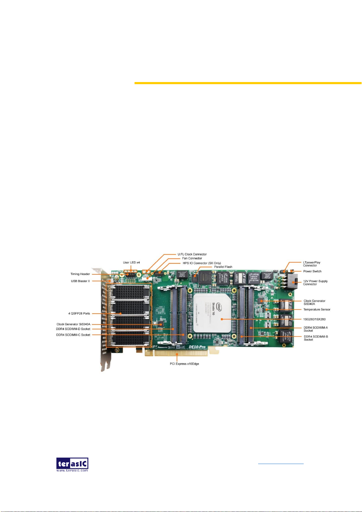
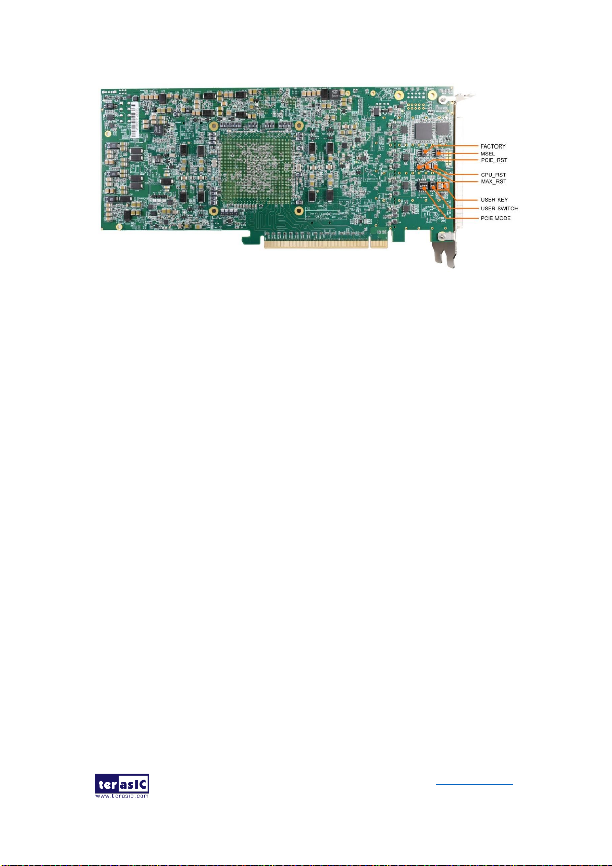
2.1 Board Overview
Figure 2-1 and Figure 2-2 is the top and bottom view of the DE10-Pro development
board. It depicts the layout of the board and indicates the location of the connectors
and key components. Users can refer to this figure for relative location of the
connectors and key components.
Figure 2-1 FPGA Board (Top)
T
DE10-Pro
User Manual
13
www.terasic.com
September 24,
2019
Figure 2-2 FPGA Board (Bottom)
2.2 Configuration, Status and Setup
◼ Configure
The FPGA board supports two configuration methods for the Stratix 10 GX/SX FPGA:
⚫ Configure the FPGA using the on-board USB-Blaster II.
⚫ Flash memory configuration of the FPGA using stored images from the
flash memory on power-up.
For programming by on-board USB-Blaster II, the following procedures show how to
download a configuration bit stream into the Stratix 10 GX/SX FPGA:
⚫ Make sure that power is provided to the FPGA board
⚫ Connect your PC to the FPGA board using a micro-USB cable and ma
ke sure the USB-Blaster II driver is installed on PC.
⚫ Launch Quartus Prime programmer and make sure the USB-Blaster II i
s detected.
⚫ In Quartus Prime Programmer, add the configuration bit stream file (.so
f), check the associated “Program/Configure” item, and click “Start” to s
tart FPGA programming.

DE10-Pro
User Manual
14
www.terasic.com
September 24,
2019
◼ Status LED
The FPGA Board development board includes board-specific status LEDs to indicate
board status. Please refer to Table 2-1 for the description of the LED indicator.
Table 2-1 Status LED
Board
Reference
LED Name
Description
D6
12-V Power
Illuminates when 12-V power is active.
D5
3.3-V Power
Illuminates when 3.3-V power is active.
D4
CONF DONE
Illuminates when the FPGA is successfully
configured. Driven by the MAX V CPLD 5M2210
System Controller.
D3
Loading
Illuminates when the MAX V CPLD 5M2210 System
Controller is actively configuring the FPGA. Driven
by the MAX 10 CPLD 10M04SCU169 System
Controller with the Embedded Blaster CPLD.
D2
Error
Illuminates when the MAX 10 CPLD 10M04SCU169
System Controller fails to configure the FPGA.
Driven by the MAX 10 CPLD 10M04SCU169
System Controller.
D1
PAGE
Illuminates when FPGA is configured by the factory
configuration bit stream.
◼ Setup PCI Express Control DIP switch
The PCI Express Control DIP switch (SW6) is provided to enable or disable different
configurations of the PCIe Connector. Table 2-2 lists the switch controls and
description.
Table 2-2 SW6 PCIe Control DIP Switch
Board
Reference
Signal Name
Description
Default
SW6.1
PCIE_PRSNT2n_x1
On : Enable x1 presence detect
Off: Disable x1 presence detect
Off
SW6.2
PCIE_PRSNT2n_x4
On : Enable x4 presence detect
Off: Disable x4 presence detect
Off

DE10-Pro
User Manual
15
www.terasic.com
September 24,
2019
SW6.3
PCIE_PRSNT2n_x8
On : Enable x8 presence detect
Off: Disable x8 presence detect
Off
SW6.4
PCIE_PRSNT2n_x16
On : Enable x16 presence detect
Off: Disable x16 presence detect
On
◼ Setup Configure Mode
The SW4 and SW5 slide switches are used to specify the configuration mode of the
FPGA. As currently only Avalon-ST x8 mode is supported, please set MSEL[2:0] to 110
positions as shown in Figure 2-3.
Figure 2-3 Position of slide switches SW4 and SW5 for Configuration Mode
◼ Select Flash Image for Configuration
The one position of slide switch SW4 is used to specify the image for configuration of
the FPGA. Setting Position FACTORY of SW4 to “1” (down position) specifies the
default factory image to be loaded, as shown in Figure 2-4. Setting Position FACTORY
of SW4 to “0” (up position) specifies the DE10-Pro to load a user-defined image, as
shown in Figure 2-5.

DE10-Pro
User Manual
16
www.terasic.com
September 24,
2019
Figure 2-4 FACTORY position of slide switch SW4 for Image Select – Factory
Image Load
Figure 2-5 FACTORY position of slide switch SW4 for Image Select – User Image
Load

DE10-Pro
User Manual
17
www.terasic.com
September 24,
2019
2.3 General User Input/Output
This section describes the user I/O interface of the FPGA.
◼ User Defined Push-buttons
The FPGA board includes two user defined push-buttons that allow users to interact
with the Stratix 10 GX/SX device. Each push-button provides a high logic level or a low
logic level when it is not pressed or pressed, respectively. Table 2-3 lists the board
references, signal names and their corresponding Stratix 10 GX/SX device pin
numbers.
Table 2-3 Push-button Pin Assignments, Schematic Signal Names, and
Functions
Board
Reference
Schematic
Signal
Name
Description
I/O
Standard
Stratix 10
GX/SX
Pin Number
PB0
BUTTON0
High Logic Level when the button
is not pressed
1.8-V
PIN_D24
PB1
BUTTON1
1.8-V
PIN_D23
◼ User-Defined Dip Switch
There are two positions dip switch (SW0) on the FPGA board to provide additional
FPGA input control. When a position of dip switch is in the DOWN position or the
UPPER position, it provides a low logic level or a high logic level to the Stratix 10
GX/SX FPGA, respectively, as shown in Figure 2-6.
Figure 2-6 One Dip switch

DE10-Pro
User Manual
18
www.terasic.com
September 24,
2019
Table 2-4 lists the signal names and their corresponding Stratix 10 GX/SX device pin
numbers.
Table 2-4 Dip Switch Pin Assignments, Schematic Signal Names, and Functions
Board
Reference
Schematic
Signal Name
Description
I/O
Standard
Stratix 10
GX/SX
Pin Number
SW0
SW0
High logic level when SW in the
UPPER position.
1.8-V
PIN_C23
SW1
SW1
1.8-V
PIN_B23
◼ User-Defined LEDs
The FPGA board consists of 4 user-controllable LEDs to allow status and debugging
signals to be driven to the LEDs from the designs loaded into the Stratix 10 GX/SX
device. Each LED is driven directly by the Stratix 10 GX/SX FPGA. The LED is turned
on or off when the associated pins are driven to a low or high logic level, respectively. A
list of the pin names on the FPGA that are connected to the LEDs is given in Table 2-5.
Table 2-5 User LEDs Pin Assignments, Schematic Signal Names, and Functions
Board
Reference
Schematic
Signal Name
Description
I/O
Standard
Stratix 10
GX/SX Pin
Number
LED0
LED0
Driving a logic 0 on the I/O
port turns the LED ON.
Driving a logic 1 on the I/O
port turns the LED OFF.
1.8-V
PIN_B24
LED1
LED1
1.8-V
PIN_A24
LED2
LED2
1.8-V
PIN_A25
LED3
LED3
1.8-V
PIN_A26
◼ 2x5 GPIO Header (Timing Expansion Header)
The FPGA board has one 2x5 GPIO header J5 for expansion function. The pin-out of
J5 is shown in Figure 2-7. GPIO_P0 ~ GPIO_P3 are bi-direction 1.8V GPIO.
GPIO_CLK0 and GPIO_CLK1 are connected to FPGA dedicated clock input and can
be configured as two single-ended clock signals. Users can use Terasic defined
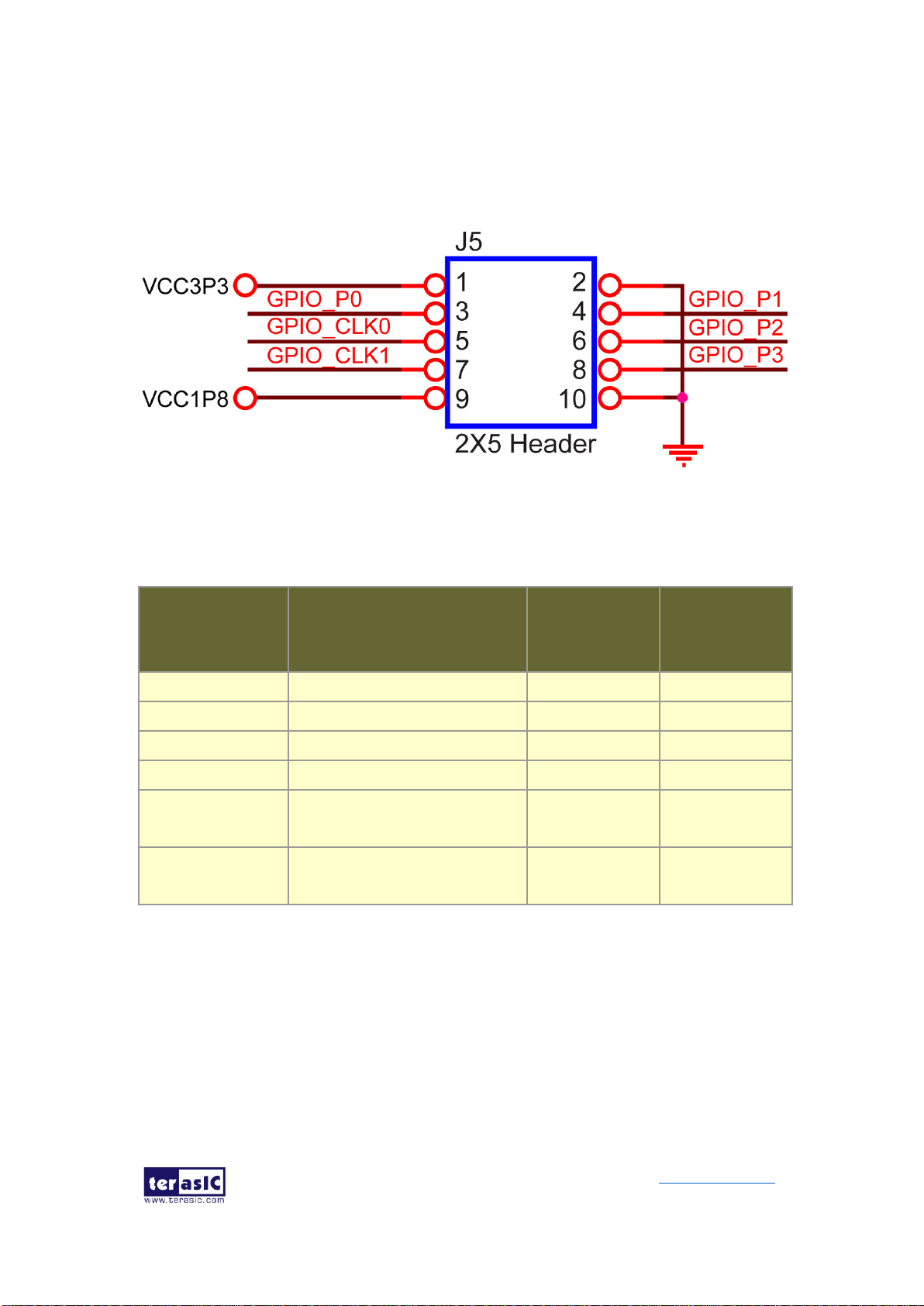
DE10-Pro
User Manual
19
www.terasic.com
September 24,
2019
RS422-RJ45 board and TUB (Timing and UART Board) for RS422 and external clock
inputs/UART applications.
Table 2-6 shows the mapping of the FPGA pin assignments to the 2x5 GPIO header.
Figure 2-7 Pin-out of 2x5 expansion header J5
Table 2-6 2x5 GPIO Header Pin Assignments, Schematic Signal Names, and
Functions
Schematic
Signal Name
Description
I/O Standard
Stratix 10
GX/SX Pin
Number
GPIO_P0
Bi-direction 1.8V GPIO
1.8-V
PIN_BB25
GPIO_P1
Bi-direction 1.8V GPIO
1.8-V
PIN_BC26
GPIO_P2
Bi-direction 1.8V GPIO
1.8-V
PIN_BC25
GPIO_P3
Bi-direction 1.8V GPIO
1.8-V
PIN_BA25
GPIO_CLK0
FPGA dedicated clock input or
Bi-direction 1.8V GPIO
1.8-V
PIN_ BA27
GPIO_CLK1
FPGA dedicated clock input or
Bi-direction 1.8V GPIO
1.8-V
PIN_ BA26
2.4 Temperature Sensor and Fan Control
The FPGA board is equipped with a temperature sensor, TMP441AIDCNT, which
provides temperature sensing. These functions are accomplished by connecting the
temperature sensor to the internal temperature sensing diode of the Stratix 10 GX/SX
device. The temperature status registers of the temperature sensor can be
programmed by a two-wire I2C bus, which is connected to the Stratix 10 GX/SX FPGA.

DE10-Pro
User Manual
20
www.terasic.com
September 24,
2019
In addition, the 7-bit slave address for this sensor is set to ‘0011100b’. Figure 2-8
shows the connection between the temperature sensor and the Stratix 10 GX/SX
FPGA.
Figure 2-8 Connections between the temperature sensor and FPGA
An optional 4-pin +12V air cooler located on J1 of the FPGA board is intended to
reduce the temperature of the FPGA. The board is equipped with a Fan-Speed
regulator and monitor, MAX6651, through an I2C interface; users regulate and monitor
the speed of the fan depending on the measured system temperature. Figure 2-9
shows the connection between the Fan-Speed Regulator and Monitor and the Stratix
10 GX/SX FPGA.
Figure 2-9 Connections between the Fan-Speed Regulator/ Monitor and the
Stratix 10 GX/SX FPGA
The pin assignments for the associated interface are listed in Table 2-7.

DE10-Pro
User Manual
21
www.terasic.com
September 24,
2019
Table 2-7 Temperature Sensor and Fan Speed Control Pin Assignments,
Schematic Signal Names, and Functions
Schematic
Signal Name
Description
I/O Standard
Stratix 10
GX/SX Pin
Number
TEMPDIODEp0
Positive pin of temperature
diode in Stratix 10
-
PIN_BJ24
TEMPDIODEn0
Negative pin of temperature
diode in Stratix 10
-
PIN_BG24
TEMP_I2C_SCL
2-Wire Serial Clock
1.8-V
PIN_E22
TEMP_I2C_SDA
2-Wire Serial-Data
1.8-V
PIN_E23
FAN_I2C_SCL
2-Wire Serial Clock
1.8-V
PIN_BD26
FAN_I2C_SDA
2-Wire Serial-Data
1.8-V
PIN_BE27
FAN_ALERT_n
Active-low ALERT input
1.8-V
PIN_BE26
2.5 Power Monitor
The DE10-Pro has implemented two power monitor chips to monitor both board input
power and FPGA core power voltage and current. Figure 2-10 shows the connection
between the power monitor chip and the Stratix 10 GX/SX FPGA. The two different
LTC2945 power monitor chips share the same I2C bus with different I2C address. The
power monitor chips monitor both shunt voltage drops and input power voltage allows
user to monitor the total board power and FPGA core power consumption.
Programmable calibration value, conversion times, and averaging, combined with an
internal multiplier, enable direct readouts of current in amperes and power in watts.
Table 2-8 shows the pin assignment of the power monitor I2C bus.

DE10-Pro
User Manual
22
www.terasic.com
September 24,
2019
Figure 2-10 Connections between the Power Monitors and FPGA
Table 2-8 Pin Assignment of Power Monitor I2C bus
Schematic
Signal Name
Description
I/O
Standard
Stratix 10
GX/SX Pin
Number
POWER_MONITOR_I2C_SCL
Power Monitor SCL
1.8V
PIN_F24
POWER_MONITOR_I2C_SDA
Power Monitor SDA
1.8V
PIN_F22
POWER_MONITOR_ALERT_n
Power Monitor ALERT
1.8V
PIN_E24
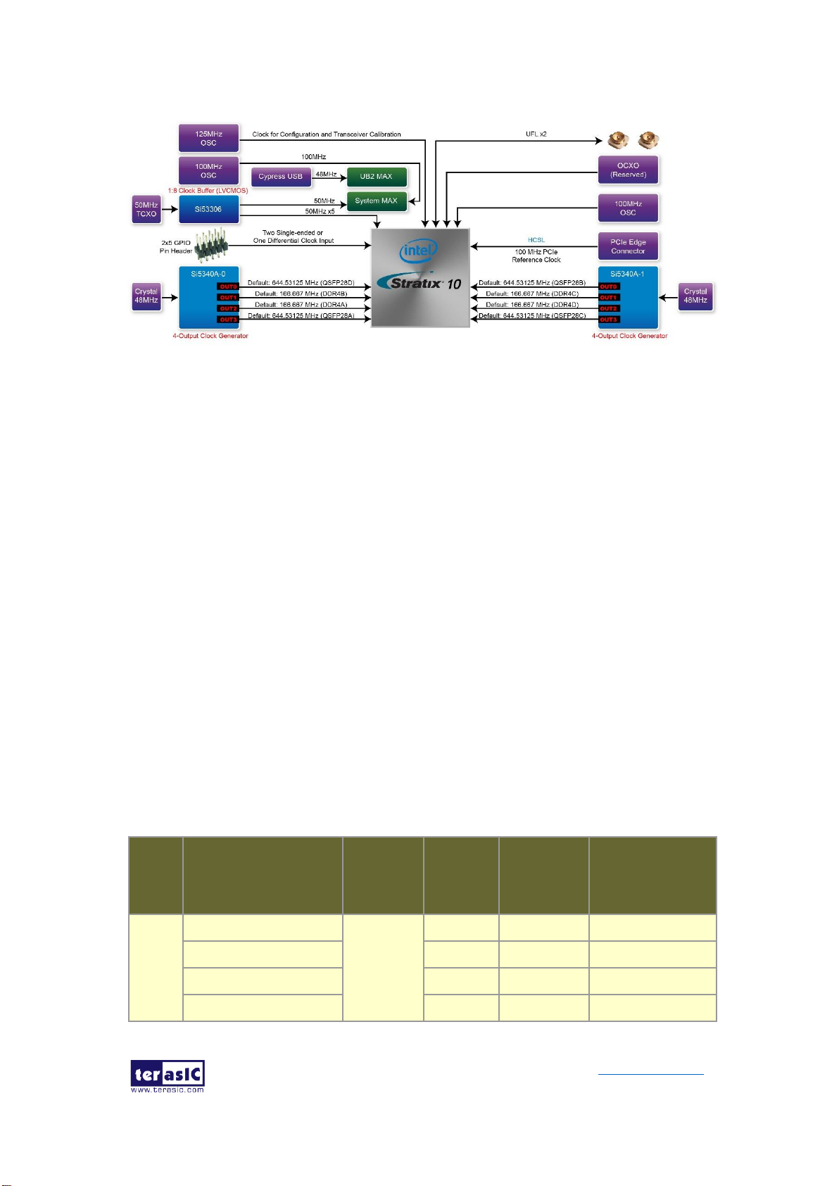
2.6 Clock Circuit
The development board includes one 50 MHz and two programmable clock generators.
Figure 2-11 shows the default frequencies of on-board all external clocks going to the
Stratix 10 GX/SX FPGA.
DE10-Pro
User Manual
23
www.terasic.com
September 24,
2019
Figure 2-11 Clock circuit of the FPGA Board
A clock buffer is used to duplicate the 50 MHz TCXO output clock, so there are five
50MHz clocks fed into different five FPGA banks. The two programming clock
generators with low-jitter clock outputs which are used to provide special and highquality clock signals for high-speed transceivers and high bandwidth memory. Through
I2C serial interface, the clock generator controllers in the Stratix 10 GX/SX FPGA can
be used to program these two Si5340As to generate 100G Ethernet QSFP28 and high
bandwidth memory reference clocks respectively. Two UFL connectors provide two
external single-ended clock inputs or one external differential clock inputs. One
oscillator provides a 125 MHz clock used as configuration clock or used as the clock
for transceiver calibration. Besides, there is one 100 MHz clock source to use as the
FPGA input clock.
Table 2-9 lists the clock source, signal names, default frequency and their
corresponding Stratix 10 GX/SX device pin numbers.
Table 2-9 Clock Source, Signal Name, Default Frequency, Pin Assignments and
Functions
Source
Schematic
Signal Name
Default
Frequency
I/O
Standard
Stratix 10
GX/SX Pin
Number
Application
Y4
CLK_50_B2C
50.0 MHz
1.2V
PIN_AW38
CLK_50_B2L
1.2V
PIN_J25
CLK_50_B3C
1.2V
PIN_BF21
CLK_50_B3L
1.2V
PIN_J20
DE10-Pro
User Manual
24
www.terasic.com
September 24,
2019
CLK_50_B3I
1.8V
PIN_M24
Y6
CLK_100_B3I
100.0MHz
1.8V
PIN_U24
J3
UFL_CLKIN_p
User
Defined
1.8V
PIN_AN27
External Clock
Input
J2
UFL_CLKIN_n
User
Defined
1.8V
PIN_AN28
External Clock
Input
U20
QSFP28A_REFCLK_p
644.53125
MHz
LVDS
PIN_T41
100G QSFP28 A
port
QSFP28D_REFCLK_p
644.53125
MHz
LVDS
PIN_T9
100G QSFP28 D
port
DDR4A_REFCLK_p
166.667
MHz
LVDS
PIN_M35
DDR4 reference
clock for A port
DDR4B_REFCLK_p
166.667
MHz
LVDS
PIN_J16
DDR4 reference
clock for B port
U28
QSFP28B_REFCLK_p
644.53125
MHz
LVDS
PIN_AM38
100G QSFP28 B
port
QSFP28C_REFCLK_p
644.53125
MHz
LVDS
PIN_AM12
100G QSFP28 C
port
DDR4C_REFCLK_p
166.667
MHz
LVDS
PIN_BH33
DDR4 reference
clock for C port
DDR4D_REFCLK_p
166.667
MHz
LVDS
PIN_AT17
QDRII+ reference
clock for D port
Table 2-10 lists the programmable oscillator control pins, signal names, I/O standard
and their corresponding Stratix 10 GX/SX device pin numbers.
Table 2-10 Programmable clock generator control pin, Signal Name, I/O standard,
Pin Assignments and Descriptions
Programmable
clock
generator
Schematic
Signal Name
I/O
Standard
Stratix 10
GX/SX Pin
Number
Description
Si5340A
(U20)
Si5340A0_I2C_SCL
1.8-V
PIN_BJ25
I2C bus, connected
with Si5340A
Si5340A0_I2C_SDA
1.8-V
PIN_BJ26
Si5340A0_RST_n
1.8-V
PIN_BH27
Si5340A reset signal
Si5340A0_INTR
1.8-V
PIN_BH26
Si5340A interrupt
signal
DE10-Pro
User Manual
25
www.terasic.com
September 24,
2019
Si5340A0_OE_n
1.8-V
PIN_BH25
Si5340A output
enable signal
Si5340A
(U28)
Si5340A1_I2C_SCL
1.8-V
PIN_G22
I2C bus, connected
with Si5340A
Si5340 A1_I2C_SDA
1.8-V
PIN_H22
Si5340A1_RST_n
1.8-V
PIN_G24
Si5340A reset signal
Si5340A1_INTR
1.8-V
PIN_H23
Si5340A interrupt
signal
Si5340A1_OE_n
1.8-V
PIN_G23
Si5340A output
enable signal
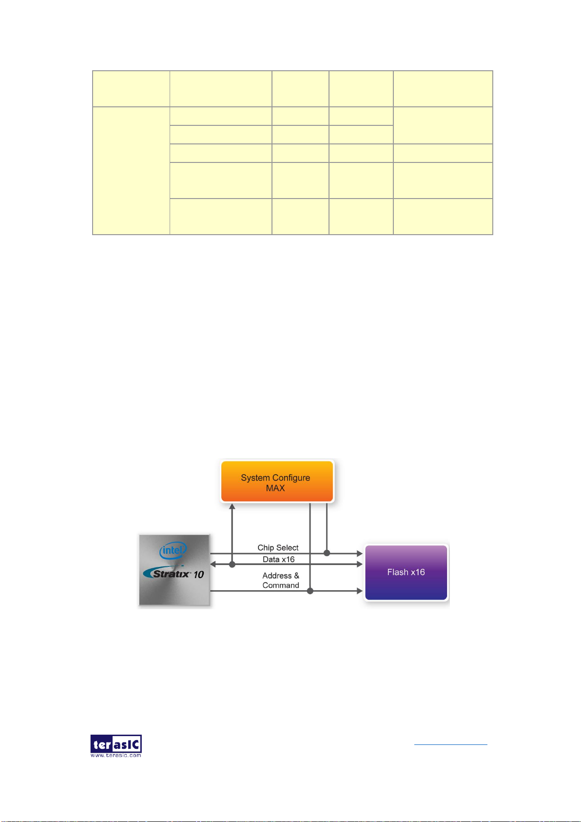
2.7 FLASH Memory
The development board has one 1Gb CFI-compatible synchronous flash devices for
non-volatile storage of FPGA configuration data, user application data, and user code
space.
The flash has a 16-bit data bus allowing for Avalon-ST x8 configuration. This device is
part of the shared flash and MAX (FM) bus, which connects to the flash memory and
MAX V CPLD (5M2210) System Controller. Figure 2-12 shows the connections
between the Flash, MAX and Stratix 10 GX/SX FPGA.
Figure 2-12 Connection between the Flash, Max and Stratix 10 GX/SX FPGA
Table 2-11 lists the flash pin assignments, signal names, and functions.

DE10-Pro
User Manual
26
www.terasic.com
September 24,
2019
Table 2-11 Flash Memory Pin Assignments, Schematic Signal Names, and
Functions
Schematic
Signal Name
Description
I/O Standard
Stratix 10 GX/SX Pin
Number
FLASH_A1
Address bus
1.8-V
PIN_V22
FLASH_A2
Address bus
1.8-V
PIN_P23
FLASH_A3
Address bus
1.8-V
PIN_K22
FLASH_A4
Address bus
1.8-V
PIN_R21
FLASH_A5
Address bus
1.8-V
PIN_K24
FLASH_A6
Address bus
1.8-V
PIN_K23
FLASH_A7
Address bus
1.8-V
PIN_R24
FLASH_A8
Address bus
1.8-V
PIN_AR28
FLASH_A9
Address bus
1.8-V
PIN_AR27
FLASH_A10
Address bus
1.8-V
PIN_AN26
FLASH_A11
Address bus
1.8-V
PIN_AP26
FLASH_A12
Address bus
1.8-V
PIN_AN25
FLASH_A13
Address bus
1.8-V
PIN_AU27
FLASH_A14
Address bus
1.8-V
PIN_AP28
FLASH_A15
Address bus
1.8-V
PIN_AT27
FLASH_A16
Address bus
1.8-V
PIN_AY28
FLASH_A17
Address bus
1.8-V
PIN_AY26
FLASH_A18
Address bus
1.8-V
PIN_AP30
FLASH_A19
Address bus
1.8-V
PIN_AW25
FLASH_A20
Address bus
1.8-V
PIN_BB27
FLASH_A21
Address bus
1.8-V
PIN_AT26
FLASH_A22
Address bus
1.8-V
PIN_AP31
FLASH_A23
Address bus
1.8-V
PIN_P24
FLASH_A24
Address bus
1.8-V
PIN_AV26
FLASH_A25
Address bus
1.8-V
PIN_AV27
FLASH_A26
Address bus
1.8-V
PIN_AP29
FLASH_A27
Address bus
1.8-V
PIN_N22
FLASH_D0
Data bus
1.8-V
PIN_N23
FLASH_D1
Data bus
1.8-V
PIN_R22

DE10-Pro
User Manual
27
www.terasic.com
September 24,
2019
FLASH_D2
Data bus
1.8-V
PIN_U20
FLASH_D3
Data bus
1.8-V
PIN_L22
FLASH_D4
Data bus
1.8-V
PIN_J23
FLASH_D5
Data bus
1.8-V
PIN_U22
FLASH_D6
Data bus
1.8-V
PIN_V23
FLASH_D7
Data bus
1.8-V
PIN_V21
FLASH_D8
Data bus
1.8-V
PIN_M23
FLASH_D9
Data bus
1.8-V
PIN_R23
FLASH_D10
Data bus
1.8-V
PIN_T20
FLASH_D11
Data bus
1.8-V
PIN_V24
FLASH_D12
Data bus
1.8-V
PIN_M22
FLASH_D13
Data bus
1.8-V
PIN_T22
FLASH_D14
Data bus
1.8-V
PIN_T21
FLASH_D15
Data bus
1.8-V
PIN_J24
FLASH_CLK
Clock
1.8-V
PIN_U23
FLASH_RESET_n
Reset
1.8-V
PIN_AP25
FLASH_CE_n
Chip enable
1.8-V
PIN_AR26
FLASH_OE_n
Output enable
1.8-V
PIN_AV25
FLASH_WE_n
Write enable
1.8-V
PIN_AT25
FLASH_ADV_n
Address valid
1.8-V
PIN_AU25
FLASH_RDY_BSY_
n
Ready of flash-0
1.8-V
PIN_AW26
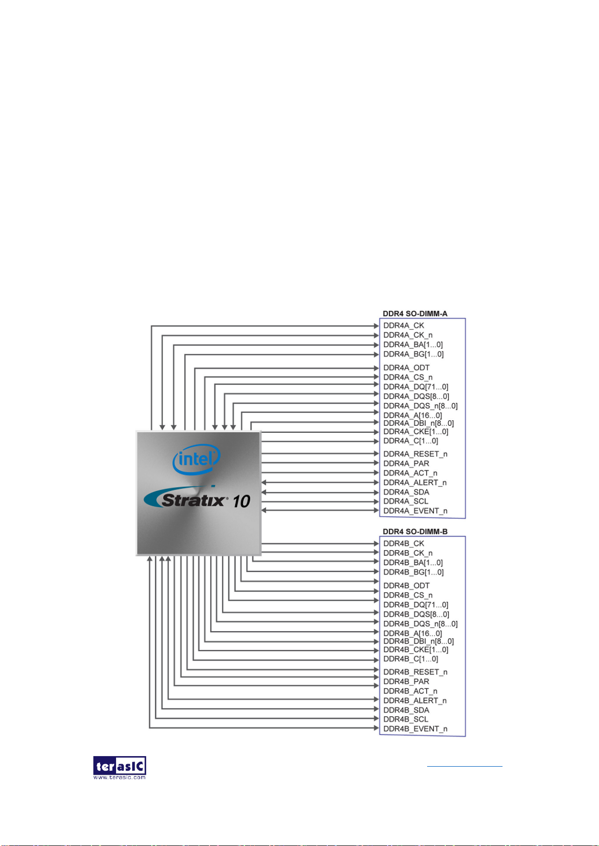
2.8 DDR4 SO-DIMM
The development board supports four independent banks of DDR4 SDRAM SO-DIMM.
Each DDR4 SODIMM socket is wired to support a maximum capacity of 8GB with ECC.
Using differential DQS signaling for the DDR4 SDRAM interfaces, it is capable of
running at up to 1333MHz memory clock for a maximum theoretical bandwidth up to
153.6Gbps. The memory clock of DDR4 SDRAM is up to 1333MHz while the FPGA
fabric speed grade is 1, and the memory clock is up to 1333MHz while the FPGA fabric
speed grade is 2. Figure 2-13 shows the connections between the DDR4 SDRAM
SO-DIMMs and Stratix 10 GX/SX FPGA.
For better flexibility in use, these four DDR4 SO-DIMM sockets also support QDRII+
DE10-Pro
User Manual
28
www.terasic.com
September 24,
2019
SRAM and QDR-IV SRAM module designed by Terasic. By using two ID pins on DDR4,
QDRII+ and QDR-IV modules, the DE10-Pro will automatically identify the memory
module type and set proper VDD and VDDQ voltage for normal operation of memory.
Each QDRII+ SO-DIMM module supports up to 576Mbits with 36-bit data width and
550 MHz clock frequency. Each QDR-IV supports up to 144Mbits with 36-bit data width
and 1066 MHz clock frequency. The four DDR4 SO-DIMM sockets are divided into
right and left groups. The two SO-DIMM sockets in the same group must be inserted
with the same memory to prevent dysfunction on memory module that requires higher
voltage. Two different memory modules can be inserted separately in right & left
groups. For example, users can insert two DDR4 modules on the right side and two
QDRII+ SRAM modules (or two QDR-IV SRAM modules) on the left side as shown in
Figure 2-14.

DE10-Pro
User Manual
29
www.terasic.com
September 24,
2019
Figure 2-13 Connection between the DDR4 and Stratix 10 GX/SX FPGA
Figure 2-14 Two memory module insertion examples
The pin assignments for DDR4 SDRAM SO-DIMM Bank-A, Bank-B, Bank-C and
Bank-D are listed in Table 2-12,Table 2-13,Table 2-14 and Table 2-15 respectively.
For QDRII+ and QDR-IV SO-DIMM module applications please refer to our example
codes in DE10-Pro CD-ROM.
Table 2-12 DDR4-A Bank Pin Assignments, Schematic Signal Names, and
Functions
Schematic
Signal Name
Description
I/O Standard
Stratix 10 GX/SX
Pin Number
DE10-Pro
User Manual
30
www.terasic.com
September 24,
2019
DDR4A_DQ0
Data [0]
1.2-V POD
PIN_A37
DDR4A_DQ1
Data [1]
1.2-V POD
PIN_B37
DDR4A_DQ2
Data [2]
1.2-V POD
PIN_B35
DDR4A_DQ3
Data [3]
1.2-V POD
PIN_C37
DDR4A_DQ4
Data [4]
1.2-V POD
PIN_B38
DDR4A_DQ5
Data [5]
1.2-V POD
PIN_C38
DDR4A_DQ6
Data [6]
1.2-V POD
PIN_C35
DDR4A_DQ7
Data [7]
1.2-V POD
PIN_D36
DDR4A_DQ8
Data [8]
1.2-V POD
PIN_H37
DDR4A_DQ9
Data [9]
1.2-V POD
PIN_E39
DDR4A_DQ10
Data [10]
1.2-V POD
PIN_E37
DDR4A_DQ11
Data [11]
1.2-V POD
PIN_D35
DDR4A_DQ12
Data [12]
1.2-V POD
PIN_E38
DDR4A_DQ13
Data [13]
1.2-V POD
PIN_D38
DDR4A_DQ14
Data [14]
1.2-V POD
PIN_D34
DDR4A_DQ15
Data [15]
1.2-V POD
PIN_F37
DDR4A_DQ16
Data [16]
1.2-V POD
PIN_F35
DDR4A_DQ17
Data [17]
1.2-V POD
PIN_J36
DDR4A_DQ18
Data [18]
1.2-V POD
PIN_J35
DDR4A_DQ19
Data [19]
1.2-V POD
PIN_E34
DDR4A_DQ20
Data [20]
1.2-V POD
PIN_G35
DDR4A_DQ21
Data [21]
1.2-V POD
PIN_H36
DDR4A_DQ22
Data [22]
1.2-V POD
PIN_H35
DDR4A_DQ23
Data [23]
1.2-V POD
PIN_H33
DDR4A_DQ24
Data [24]
1.2-V POD
PIN_N32
DDR4A_DQ25
Data [25]
1.2-V POD
PIN_M33
DDR4A_DQ26
Data [26]
1.2-V POD
PIN_K34
DDR4A_DQ27
Data [27]
1.2-V POD
PIN_M34
DDR4A_DQ28
Data [28]
1.2-V POD
PIN_N33
DDR4A_DQ29
Data [29]
1.2-V POD
PIN_N31
DDR4A_DQ30
Data [30]
1.2-V POD
PIN_K33
DDR4A_DQ31
Data [31]
1.2-V POD
PIN_K32
DDR4A_DQ32
Data [32]
1.2-V POD
PIN_M25
DDR4A_DQ33
Data [33]
1.2-V POD
PIN_P25
DDR4A_DQ34
Data [34]
1.2-V POD
PIN_T25

DE10-Pro
User Manual
31
www.terasic.com
September 24,
2019
DDR4A_DQ35
Data [35]
1.2-V POD
PIN_R26
DDR4A_DQ36
Data [36]
1.2-V POD
PIN_L25
DDR4A_DQ37
Data [37]
1.2-V POD
PIN_N27
DDR4A_DQ38
Data [38]
1.2-V POD
PIN_U25
DDR4A_DQ39
Data [39]
1.2-V POD
PIN_P26
DDR4A_DQ40
Data [40]
1.2-V POD
PIN_U27
DDR4A_DQ41
Data [41]
1.2-V POD
PIN_T29
DDR4A_DQ42
Data [42]
1.2-V POD
PIN_V25
DDR4A_DQ43
Data [43]
1.2-V POD
PIN_U29
DDR4A_DQ44
Data [44]
1.2-V POD
PIN_U28
DDR4A_DQ45
Data [45]
1.2-V POD
PIN_T30
DDR4A_DQ46
Data [46]
1.2-V POD
PIN_V26
DDR4A_DQ47
Data [47]
1.2-V POD
PIN_U30
DDR4A_DQ48
Data [48]
1.2-V POD
PIN_F25
DDR4A_DQ49
Data [49]
1.2-V POD
PIN_K27
DDR4A_DQ50
Data [50]
1.2-V POD
PIN_L27
DDR4A_DQ51
Data [51]
1.2-V POD
PIN_H26
DDR4A_DQ52
Data [52]
1.2-V POD
PIN_H25
DDR4A_DQ53
Data [53]
1.2-V POD
PIN_H27
DDR4A_DQ54
Data [54]
1.2-V POD
PIN_M27
DDR4A_DQ55
Data [55]
1.2-V POD
PIN_G25
DDR4A_DQ56
Data [56]
1.2-V POD
PIN_D26
DDR4A_DQ57
Data [57]
1.2-V POD
PIN_B27
DDR4A_DQ58
Data [58]
1.2-V POD
PIN_G27
DDR4A_DQ59
Data [59]
1.2-V POD
PIN_B25
DDR4A_DQ60
Data [60]
1.2-V POD
PIN_C27
DDR4A_DQ61
Data [61]
1.2-V POD
PIN_C26
DDR4A_DQ62
Data [62]
1.2-V POD
PIN_F27
DDR4A_DQ63
Data [63]
1.2-V POD
PIN_D25
DDR4A_DQ64
Data [64]
1.2-V POD
PIN_R31
DDR4A_DQ65
Data [65]
1.2-V POD
PIN_T34
DDR4A_DQ66
Data [66]
1.2-V POD
PIN_R34
DDR4A_DQ67
Data [67]
1.2-V POD
PIN_P33
DDR4A_DQ68
Data [68]
1.2-V POD
PIN_T31
DDR4A_DQ69
Data [69]
1.2-V POD
PIN_U33

DE10-Pro
User Manual
32
www.terasic.com
September 24,
2019
DDR4A_DQ70
Data [70]
1.2-V POD
PIN_V32
DDR4A_DQ71
Data [71]
1.2-V POD
PIN_U32
DDR4A_DQS0
Data Strobe p[0]
DIFFERENTIAL 1.2-V
POD
PIN_A36
DDR4A_DQS_n0
Data Strobe n[0]
DIFFERENTIAL 1.2-V
POD
PIN_A35
DDR4A_DQS1
Data Strobe p[1]
DIFFERENTIAL 1.2-V
POD
PIN_E36
DDR4A_DQS_n1
Data Strobe n[1]
DIFFERENTIAL 1.2-V
POD
PIN_F36
DDR4A_DQS2
Data Strobe p[2]
DIFFERENTIAL 1.2-V
POD
PIN_G33
DDR4A_DQS_n2
Data Strobe n[2]
DIFFERENTIAL 1.2-V
POD
PIN_G34
DDR4A_DQS3
Data Strobe p[3]
DIFFERENTIAL 1.2-V
POD
PIN_L32
DDR4A_DQS_n3
Data Strobe n[3]
DIFFERENTIAL 1.2-V
POD
PIN_L31
DDR4A_DQS4
Data Strobe p[4]
DIFFERENTIAL 1.2-V
POD
PIN_T26
DDR4A_DQS_n4
Data Strobe n[4]
DIFFERENTIAL 1.2-V
POD
PIN_R27
DDR4A_DQS5
Data Strobe p[5]
DIFFERENTIAL 1.2-V
POD
PIN_V28
DDR4A_DQS_n5
Data Strobe n[5]
DIFFERENTIAL 1.2-V
POD
PIN_V27
DDR4A_DQS6
Data Strobe p[6]
DIFFERENTIAL 1.2-V
POD
PIN_J26
DDR4A_DQS_n6
Data Strobe n[6]
DIFFERENTIAL 1.2-V
POD
PIN_K26
DDR4A_DQS7
Data Strobe p[7]
DIFFERENTIAL 1.2-V
POD
PIN_E26
DDR4A_DQS_n7
Data Strobe n[7]
DIFFERENTIAL 1.2-V
POD
PIN_F26
DDR4A_DQS8
Data Strobe p[8]
DIFFERENTIAL 1.2-V
POD
PIN_R32
DE10-Pro
User Manual
33
www.terasic.com
September 24,
2019
DDR4A_DQS_n8
Data Strobe n[8]
DIFFERENTIAL 1.2-V
POD
PIN_T32
DDR4A_DBI_n0
Data Bus Inversion
[0]
1.2-V POD
PIN_C36
DDR4A_DBI_n1
Data Bus Inversion
[1]
1.2-V POD
PIN_D39
DDR4A_DBI_n2
Data Bus Inversion
[2]
1.2-V POD
PIN_F34
DDR4A_DBI_n3
Data Bus Inversion
[3]
1.2-V POD
PIN_J34
DDR4A_DBI_n4
Data Bus Inversion
[4]
1.2-V POD
PIN_N25
DDR4A_DBI_n5
Data Bus Inversion
[5]
1.2-V POD
PIN_V30
DDR4A_DBI_n6
Data Bus Inversion
[6]
1.2-V POD
PIN_L26
DDR4A_DBI_n7
Data Bus Inversion
[7]
1.2-V POD
PIN_E27
DDR4A_DBI_n8
Data Bus Inversion
[8]
1.2-V POD
PIN_U34
DDR4A_A0
Address [0]
SSTL-12
PIN_K38
DDR4A_A1
Address [1]
SSTL-12
PIN_L37
DDR4A_A2
Address [2]
SSTL-12
PIN_M37
DDR4A_A3
Address [3]
SSTL-12
PIN_M38
DDR4A_A4
Address [4]
SSTL-12
PIN_J39
DDR4A_A5
Address [5]
SSTL-12
PIN_J38
DDR4A_A6
Address [6]
SSTL-12
PIN_K39
DDR4A_A7
Address [7]
SSTL-12
PIN_L39
DDR4A_A8
Address [8]
SSTL-12
PIN_P37
DDR4A_A9
Address [9]
SSTL-12
PIN_R37
DDR4A_A10
Address [10]
SSTL-12
PIN_N37
DDR4A_A11
Address [11]
SSTL-12
PIN_P38
DDR4A_A12
Address [12]
SSTL-12
PIN_P35
DDR4A_A13
Address [13]
SSTL-12
PIN_K36
DDR4A_A14
Address [14]/
SSTL-12
PIN_K37

DE10-Pro
User Manual
34
www.terasic.com
September 24,
2019
WE_n
DDR4A_A15
Address [15]/
CAS_n
SSTL-12
PIN_N36
DDR4A_A16
Address [16]/
RAS_n
SSTL-12
PIN_P36
DDR4A_BA0
Bank Select [0]
SSTL-12
PIN_L36
DDR4A_BA1
Bank Select [1]
SSTL-12
PIN_T35
DDR4A_BG0
Bank Group Select
[0]
SSTL-12
PIN_R36
DDR4A_BG1
Bank Group Select
[1]
SSTL-12
PIN_D40
DDR4A_C0
Chip ID 0
SSTL-12
PIN_F40
DDR4A_C1
Chip ID 1
SSTL-12
PIN_K40
DDR4A_CK
Clock p
DIFFERENTIAL 1.2-V
SSTL
PIN_F39
DDR4A_CK_n
Clock n
DIFFERENTIAL 1.2-V
SSTL
PIN_G39
DDR4A_CKE
Clock Enable pin
SSTL-12
PIN_L40
DDR4A_ODT
On Die
Termination
SSTL-12
PIN_G40
DDR4A_CS_n
Chip Select
SSTL-12
PIN_G38
DDR4A_PAR
Command and
Address Parity
Input
SSTL-12
PIN_H40
DDR4A_ALERT_n
Register ALERT_n
output
1.2 V
PIN_A38
DDR4A_ACT_n
Activation
Command Input
SSTL-12
PIN_H38
DDR4A_RESET_n
Chip Reset
1.2 V
PIN_E40
DDR4A_EVENT_n
Chip Temperature
Event
1.2 V
PIN_J33
DDR4A_SDA
Chip I2C Serial
Data Bus
1.2 V
PIN_T24
DDR4A_SCL
Chip I2C Serial
Clock
1.2 V
PIN_L24

DE10-Pro
User Manual
35
www.terasic.com
September 24,
2019
DDR4A_REFCLK_p
DDR4 A port
Reference Clock p
LVDS
PIN_M35
DDR4A_REFCLK_n
DDR4 A port
Reference Clock n
LVDS
PIN_N35
Table 2-13 DDR4-B Pin Assignments, Schematic Signal Names, and Functions
Schematic
Signal Name
Description
I/O Standard
Stratix 10
GX/SX Pin
Number
DDR4B_DQ0
Data [0]
1.2-V POD
PIN_T16
DDR4B_DQ1
Data [1]
1.2-V POD
PIN_V18
DDR4B_DQ2
Data [2]
1.2-V POD
PIN_R19
DDR4B_DQ3
Data [3]
1.2-V POD
PIN_U18
DDR4B_DQ4
Data [4]
1.2-V POD
PIN_U19
DDR4B_DQ5
Data [5]
1.2-V POD
PIN_W18
DDR4B_DQ6
Data [6]
1.2-V POD
PIN_R18
DDR4B_DQ7
Data [7]
1.2-V POD
PIN_V17
DDR4B_DQ8
Data [8]
1.2-V POD
PIN_P16
DDR4B_DQ9
Data [9]
1.2-V POD
PIN_P14
DDR4B_DQ10
Data [10]
1.2-V POD
PIN_P15
DDR4B_DQ11
Data [11]
1.2-V POD
PIN_R13
DDR4B_DQ12
Data [12]
1.2-V POD
PIN_R17
DDR4B_DQ13
Data [13]
1.2-V POD
PIN_N13
DDR4B_DQ14
Data [14]
1.2-V POD
PIN_R14
DDR4B_DQ15
Data [15]
1.2-V POD
PIN_M13
DDR4B_DQ16
Data [16]
1.2-V POD
PIN_J11
DDR4B_DQ17
Data [17]
1.2-V POD
PIN_K10
DDR4B_DQ18
Data [18]
1.2-V POD
PIN_K11
DDR4B_DQ19
Data [19]
1.2-V POD
PIN_J13
DDR4B_DQ20
Data [20]
1.2-V POD
PIN_K13
DDR4B_DQ21
Data [21]
1.2-V POD
PIN_L10
DDR4B_DQ22
Data [22]
1.2-V POD
PIN_K12
DDR4B_DQ23
Data [23]
1.2-V POD
PIN_H11
DDR4B_DQ24
Data [24]
1.2-V POD
PIN_F10
DDR4B_DQ25
Data [25]
1.2-V POD
PIN_E10

DE10-Pro
User Manual
36
www.terasic.com
September 24,
2019
DDR4B_DQ26
Data [26]
1.2-V POD
PIN_H10
DDR4B_DQ27
Data [27]
1.2-V POD
PIN_F12
DDR4B_DQ28
Data [28]
1.2-V POD
PIN_G10
DDR4B_DQ29
Data [29]
1.2-V POD
PIN_F11
DDR4B_DQ30
Data [30]
1.2-V POD
PIN_E11
DDR4B_DQ31
Data [31]
1.2-V POD
PIN_E12
DDR4B_DQ32
Data [32]
1.2-V POD
PIN_N20
DDR4B_DQ33
Data [33]
1.2-V POD
PIN_H21
DDR4B_DQ34
Data [34]
1.2-V POD
PIN_P21
DDR4B_DQ35
Data [35]
1.2-V POD
PIN_K19
DDR4B_DQ36
Data [36]
1.2-V POD
PIN_K21
DDR4B_DQ37
Data [37]
1.2-V POD
PIN_J21
DDR4B_DQ38
Data [38]
1.2-V POD
PIN_N21
DDR4B_DQ39
Data [39]
1.2-V POD
PIN_L19
DDR4B_DQ40
Data [40]
1.2-V POD
PIN_H18
DDR4B_DQ41
Data [41]
1.2-V POD
PIN_G19
DDR4B_DQ42
Data [42]
1.2-V POD
PIN_J18
DDR4B_DQ43
Data [43]
1.2-V POD
PIN_G20
DDR4B_DQ44
Data [44]
1.2-V POD
PIN_G18
DDR4B_DQ45
Data [45]
1.2-V POD
PIN_F19
DDR4B_DQ46
Data [46]
1.2-V POD
PIN_K18
DDR4B_DQ47
Data [47]
1.2-V POD
PIN_H20
DDR4B_DQ48
Data [48]
1.2-V POD
PIN_E17
DDR4B_DQ49
Data [49]
1.2-V POD
PIN_D21
DDR4B_DQ50
Data [50]
1.2-V POD
PIN_E18
DDR4B_DQ51
Data [51]
1.2-V POD
PIN_C22
DDR4B_DQ52
Data [52]
1.2-V POD
PIN_D19
DDR4B_DQ53
Data [53]
1.2-V POD
PIN_F17
DDR4B_DQ54
Data [54]
1.2-V POD
PIN_D18
DDR4B_DQ55
Data [55]
1.2-V POD
PIN_C21
DDR4B_DQ56
Data [56]
1.2-V POD
PIN_B20
DDR4B_DQ57
Data [57]
1.2-V POD
PIN_B18
DDR4B_DQ58
Data [58]
1.2-V POD
PIN_B22
DDR4B_DQ59
Data [59]
1.2-V POD
PIN_A17
DDR4B_DQ60
Data [60]
1.2-V POD
PIN_B19

DE10-Pro
User Manual
37
www.terasic.com
September 24,
2019
DDR4B_DQ61
Data [61]
1.2-V POD
PIN_A20
DDR4B_DQ62
Data [62]
1.2-V POD
PIN_A22
DDR4B_DQ63
Data [63]
1.2-V POD
PIN_A19
DDR4B_DQ64
Data [64]
1.2-V POD
PIN_P18
DDR4B_DQ65
Data [65]
1.2-V POD
PIN_K16
DDR4B_DQ66
Data [66]
1.2-V POD
PIN_M15
DDR4B_DQ67
Data [67]
1.2-V POD
PIN_M18
DDR4B_DQ68
Data [68]
1.2-V POD
PIN_N16
DDR4B_DQ69
Data [69]
1.2-V POD
PIN_L16
DDR4B_DQ70
Data [70]
1.2-V POD
PIN_N18
DDR4B_DQ71
Data [71]
1.2-V POD
PIN_M17
DDR4B_DQS0
Data Strobe p[0]
DIFFERENTIAL 1.2-V
POD
PIN_U17
DDR4B_DQS_n0
Data Strobe n[0]
DIFFERENTIAL 1.2-V
POD
PIN_T17
DDR4B_DQS1
Data Strobe p[1]
DIFFERENTIAL 1.2-V
POD
PIN_P12
DDR4B_DQS_n1
Data Strobe n[1]
DIFFERENTIAL 1.2-V
POD
PIN_P13
DDR4B_DQS2
Data Strobe p[2]
DIFFERENTIAL 1.2-V
POD
PIN_L12
DDR4B_DQS_n2
Data Strobe n[2]
DIFFERENTIAL 1.2-V
POD
PIN_M12
DDR4B_DQS3
Data Strobe p[3]
DIFFERENTIAL 1.2-V
POD
PIN_H12
DDR4B_DQS_n3
Data Strobe n[3]
DIFFERENTIAL 1.2-V
POD
PIN_G12
DDR4B_DQS4
Data Strobe p[4]
DIFFERENTIAL 1.2-V
POD
PIN_M20
DDR4B_DQS_n4
Data Strobe n[4]
DIFFERENTIAL 1.2-V
POD
PIN_L20
DDR4B_DQS5
Data Strobe p[5]
DIFFERENTIAL 1.2-V
POD
PIN_F20
DDR4B_DQS_n5
Data Strobe n[5]
DIFFERENTIAL 1.2-V
POD
PIN_F21
DE10-Pro
User Manual
38
www.terasic.com
September 24,
2019
DDR4B_DQS6
Data Strobe p[6]
DIFFERENTIAL 1.2-V
POD
PIN_D20
DDR4B_DQS_n6
Data Strobe n[6]
DIFFERENTIAL 1.2-V
POD
PIN_C20
DDR4B_DQS7
Data Strobe p[7]
DIFFERENTIAL 1.2-V
POD
PIN_C17
DDR4B_DQS_n7
Data Strobe n[7]
DIFFERENTIAL 1.2-V
POD
PIN_C18
DDR4B_DQS8
Data Strobe p[8]
DIFFERENTIAL 1.2-V
POD
PIN_L17
DDR4B_DQS_n8
Data Strobe n[8]
DIFFERENTIAL 1.2-V
POD
PIN_K17
DDR4B_DBI_n0
Data Bus Inversion
[0]
1.2-V POD
PIN_T19
DDR4B_DBI_n1
Data Bus Inversion
[1]
1.2-V POD
PIN_ M14
DDR4B_DBI_n2
Data Bus Inversion
[2]
1.2-V POD
PIN_J10
DDR4B_DBI_n3
Data Bus Inversion
[3]
1.2-V POD
PIN_D11
DDR4B_DBI_n4
Data Bus Inversion
[4]
1.2-V POD
PIN_L21
DDR4B_DBI_n5
Data Bus Inversion
[5]
1.2-V POD
PIN_J19
DDR4B_DBI_n6
Data Bus Inversion
[6]
1.2-V POD
PIN_E19
DDR4B_DBI_n7
Data Bus Inversion
[7]
1.2-V POD
PIN_A21
DDR4B_DBI_n8
Data Bus Inversion
[8]
1.2-V POD
PIN_N15
DDR4B_A0
Address [0]
SSTL-12
PIN_C16
DDR4B_A1
Address [1]
SSTL-12
PIN_D16
DDR4B_A2
Address [2]
SSTL-12
PIN_A14
DDR4B_A3
Address [3]
SSTL-12
PIN_A15
DDR4B_A4
Address [4]
SSTL-12
PIN_B14
DE10-Pro
User Manual
39
www.terasic.com
September 24,
2019
DDR4B_A5
Address [5]
SSTL-12
PIN_B13
DDR4B_A6
Address [6]
SSTL-12
PIN_A16
DDR4B_A7
Address [7]
SSTL-12
PIN_B15
DDR4B_A8
Address [8]
SSTL-12
PIN_C15
DDR4B_A9
Address [9]
SSTL-12
PIN_D15
DDR4B_A10
Address [10]
SSTL-12
PIN_E16
DDR4B_A11
Address [11]
SSTL-12
PIN_F16
DDR4B_A12
Address [12]
SSTL-12
PIN_L14
DDR4B_A13
Address [13]
SSTL-12
PIN_H15
DDR4B_A14
Address [14]/
WE_n
SSTL-12
PIN_J15
DDR4B_A15
Address [15]/
CAS_n
SSTL-12
PIN_G15
DDR4B_A16
Address [16]/
RAS_n
SSTL-12
PIN_F15
DDR4B_BA0
Bank Select [0]
SSTL-12
PIN_H17
DDR4B_BA1
Bank Select [1]
SSTL-12
PIN_K14
DDR4B_BG0
Bank Group Select
[0]
SSTL-12
PIN_J14
DDR4B_BG1
Bank Group Select
[1]
SSTL-12
PIN_G13
DDR4B_C0
Chip ID 0
SSTL-12
PIN_F14
DDR4B_C1
Chip ID 1
SSTL-12
PIN_C12
DDR4B_CK
Clock p
DIFFERENTIAL 1.2-V
SSTL
PIN_E14
DDR4B_CK_n
Clock n
DIFFERENTIAL 1.2-V
SSTL
PIN_D14
DDR4B_CKE
Clock Enable pin
SSTL-12
PIN_ C13
DDR4B_ODT
On Die
Termination
SSTL-12
PIN_G14
DDR4B_CS_n
Chip Select
SSTL-12
PIN_E13
DDR4B_PAR
Command and
Address Parity
Input
SSTL-12
PIN_A12
DDR4B_ALERT_n
Register ALERT_n
1.2 V
PIN_T15

DE10-Pro
User Manual
40
www.terasic.com
September 24,
2019
output
DDR4B_ACT_n
Activation
Command Input
SSTL-12
PIN_D13
DDR4B_RESET_n
Chip Reset
1.2 V
PIN_H13
DDR4B_EVENT_n
Chip Temperature
Event
1.2 V
PIN_L11
DDR4B_SDA
Chip I2C Serial
Data Bus
1.2 V
PIN_P20
DDR4B_SCL
Chip I2C Serial
Clock
1.2 V
PIN_D10
DDR4B_REFCLK_p
DDR4 B port
Reference Clock p
LVDS
PIN_J16
DDR4B_REFCLK_n
DDR4 B port
Reference Clock n
LVDS
PIN_H16
Table 2-14 DDR4-C Pin Assignments, Schematic Signal Names, and Functions
Schematic
Signal Name
Description
I/O Standard
Stratix 10
GX/SX Pin
Number
DDR4C_DQ0
Data [0]
1.2-V POD
PIN_AP35
DDR4C_DQ1
Data [1]
1.2-V POD
PIN_AT38
DDR4C_DQ2
Data [2]
1.2-V POD
PIN_AP36
DDR4C_DQ3
Data [3]
1.2-V POD
PIN_AR33
DDR4C_DQ4
Data [4]
1.2-V POD
PIN_AN33
DDR4C_DQ5
Data [5]
1.2-V POD
PIN_AR37
DDR4C_DQ6
Data [6]
1.2-V POD
PIN_AR36
DDR4C_DQ7
Data [7]
1.2-V POD
PIN_AR34
DDR4C_DQ8
Data [8]
1.2-V POD
PIN_AU38
DDR4C_DQ9
Data [9]
1.2-V POD
PIN_AV40
DDR4C_DQ10
Data [10]
1.2-V POD
PIN_AW40
DDR4C_DQ11
Data [11]
1.2-V POD
PIN_AV37
DDR4C_DQ12
Data [12]
1.2-V POD
PIN_AU37
DDR4C_DQ13
Data [13]
1.2-V POD
PIN_AW39
DDR4C_DQ14
Data [14]
1.2-V POD
PIN_AV38
DDR4C_DQ15
Data [15]
1.2-V POD
PIN_BA37

DE10-Pro
User Manual
41
www.terasic.com
September 24,
2019
DDR4C_DQ16
Data [16]
1.2-V POD
PIN_BD40
DDR4C_DQ17
Data [17]
1.2-V POD
PIN_BF39
DDR4C_DQ18
Data [18]
1.2-V POD
PIN_BG38
DDR4C_DQ19
Data [19]
1.2-V POD
PIN_BH36
DDR4C_DQ20
Data [20]
1.2-V POD
PIN_BE38
DDR4C_DQ21
Data [21]
1.2-V POD
PIN_BE39
DDR4C_DQ22
Data [22]
1.2-V POD
PIN_BG37
DDR4C_DQ23
Data [23]
1.2-V POD
PIN_BH37
DDR4C_DQ24
Data [24]
1.2-V POD
PIN_BB38
DDR4C_DQ25
Data [25]
1.2-V POD
PIN_BB39
DDR4C_DQ26
Data [26]
1.2-V POD
PIN_BC38
DDR4C_DQ27
Data [27]
1.2-V POD
PIN_BC37
DDR4C_DQ28
Data [28]
1.2-V POD
PIN_BA40
DDR4C_DQ29
Data [29]
1.2-V POD
PIN_AY40
DDR4C_DQ30
Data [30]
1.2-V POD
PIN_BC40
DDR4C_DQ31
Data [31]
1.2-V POD
PIN_BB37
DDR4C_DQ32
Data [32]
1.2-V POD
PIN_BF29
DDR4C_DQ33
Data [33]
1.2-V POD
PIN_BE28
DDR4C_DQ34
Data [34]
1.2-V POD
PIN_BJ28
DDR4C_DQ35
Data [35]
1.2-V POD
PIN_BJ30
DDR4C_DQ36
Data [36]
1.2-V POD
PIN_BE32
DDR4C_DQ37
Data [37]
1.2-V POD
PIN_BG32
DDR4C_DQ38
Data [38]
1.2-V POD
PIN_BH28
DDR4C_DQ39
Data [39]
1.2-V POD
PIN_BJ29
DDR4C_DQ40
Data [40]
1.2-V POD
PIN_BE31
DDR4C_DQ41
Data [41]
1.2-V POD
PIN_BD29
DDR4C_DQ42
Data [42]
1.2-V POD
PIN_BF31
DDR4C_DQ43
Data [43]
1.2-V POD
PIN_BG30
DDR4C_DQ44
Data [44]
1.2-V POD
PIN_BF30
DDR4C_DQ45
Data [45]
1.2-V POD
PIN_BE29
DDR4C_DQ46
Data [46]
1.2-V POD
PIN_BG29
DDR4C_DQ47
Data [47]
1.2-V POD
PIN_BH30
DDR4C_DQ48
Data [48]
1.2-V POD
PIN_BA31
DDR4C_DQ49
Data [49]
1.2-V POD
PIN_BC32
DDR4C_DQ50
Data [50]
1.2-V POD
PIN_BB30
DE10-Pro
User Manual
42
www.terasic.com
September 24,
2019
DDR4C_DQ51
Data [51]
1.2-V POD
PIN_AW31
DDR4C_DQ52
Data [52]
1.2-V POD
PIN_BC31
DDR4C_DQ53
Data [53]
1.2-V POD
PIN_AY32
DDR4C_DQ54
Data [54]
1.2-V POD
PIN_BB29
DDR4C_DQ55
Data [55]
1.2-V POD
PIN_BA30
DDR4C_DQ56
Data [56]
1.2-V POD
PIN_AU28
DDR4C_DQ57
Data [57]
1.2-V POD
PIN_AT29
DDR4C_DQ58
Data [58]
1.2-V POD
PIN_AW29
DDR4C_DQ59
Data [59]
1.2-V POD
PIN_AY29
DDR4C_DQ60
Data [60]
1.2-V POD
PIN_AT30
DDR4C_DQ61
Data [61]
1.2-V POD
PIN_AU29
DDR4C_DQ62
Data [62]
1.2-V POD
PIN_AU30
DDR4C_DQ63
Data [63]
1.2-V POD
PIN_BA29
DDR4C_DQ64
Data [64]
1.2-V POD
PIN_BD36
DDR4C_DQ65
Data [65]
1.2-V POD
PIN_BF35
DDR4C_DQ66
Data [66]
1.2-V POD
PIN_BC36
DDR4C_DQ67
Data [67]
1.2-V POD
PIN_BD33
DDR4C_DQ68
Data [68]
1.2-V POD
PIN_BE36
DDR4C_DQ69
Data [69]
1.2-V POD
PIN_BF36
DDR4C_DQ70
Data [70]
1.2-V POD
PIN_BB34
DDR4C_DQ71
Data [71]
1.2-V POD
PIN_BB33
DDR4C_DQS0
Data Strobe p[0]
DIFFERENTIAL 1.2-V
POD
PIN_AT37
DDR4C_DQS_n0
Data Strobe n[0]
DIFFERENTIAL 1.2-V
POD
PIN_AT36
DDR4C_DQS1
Data Strobe p[1]
DIFFERENTIAL 1.2-V
POD
PIN_AY38
DDR4C_DQS_n1
Data Strobe n[1]
DIFFERENTIAL 1.2-V
POD
PIN_AY39
DDR4C_DQS2
Data Strobe p[2]
DIFFERENTIAL 1.2-V
POD
PIN_BF37
DDR4C_DQS_n2
Data Strobe n[2]
DIFFERENTIAL 1.2-V
POD
PIN_BE37
DDR4C_DQS3
Data Strobe p[3]
DIFFERENTIAL 1.2-V
POD
PIN_BD39

DE10-Pro
User Manual
43
www.terasic.com
September 24,
2019
DDR4C_DQS_n3
Data Strobe n[3]
DIFFERENTIAL 1.2-V
POD
PIN_BD38
DDR4C_DQS4
Data Strobe p[3]
DIFFERENTIAL 1.2-V
POD
PIN_BH31
DDR4C_DQS_n4
Data Strobe n[4]
DIFFERENTIAL 1.2-V
POD
PIN_BJ31
DDR4C_DQS5
Data Strobe p[5]
DIFFERENTIAL 1.2-V
POD
PIN_BC30
DDR4C_DQS_n5
Data Strobe n[5]
DIFFERENTIAL 1.2-V
POD
PIN_BD30
DDR4C_DQS6
Data Strobe p[6]
DIFFERENTIAL 1.2-V
POD
PIN_BA32
DDR4C_DQS_n6
Data Strobe n[6]
DIFFERENTIAL 1.2-V
POD
PIN_BB32
DDR4C_DQS7
Data Strobe p[7]
DIFFERENTIAL 1.2-V
POD
PIN_AW28
DDR4C_DQS_n7
Data Strobe n[7]
DIFFERENTIAL 1.2-V
POD
PIN_AV28
DDR4C_DQS8
Data Strobe p[8]
DIFFERENTIAL 1.2-V
POD
PIN_BD34
DDR4C_DQS_n8
Data Strobe n[8]
DIFFERENTIAL 1.2-V
POD
PIN_BD35
DDR4C_DBI_n0
Data Bus Inversion
[0]
1.2-V POD
PIN_AP33
DDR4C_DBI_n1
Data Bus Inversion
[1]
1.2-V POD
PIN_AY37
DDR4C_DBI_n2
Data Bus Inversion
[2]
1.2-V POD
PIN_BE40
DDR4C_DBI_n3
Data Bus Inversion
[3]
1.2-V POD
PIN_BB40
DDR4C_DBI_n4
Data Bus Inversion
[4]
1.2-V POD
PIN_BF32
DDR4C_DBI_n5
Data Bus Inversion
[5]
1.2-V POD
PIN_BD31
DDR4C_DBI_n6
Data Bus Inversion
[6]
1.2-V POD
PIN_AW30
DE10-Pro
User Manual
44
www.terasic.com
September 24,
2019
DDR4C_DBI_n7
Data Bus Inversion
[7]
1.2-V POD
PIN_AV30
DDR4C_DBI_n8
Data Bus Inversion
[8]
1.2-V POD
PIN_BC35
DDR4C_A0
Address [0]
SSTL-12
PIN_AY34
DDR4C_A1
Address [1]
SSTL-12
PIN_BA34
DDR4C_A2
Address [2]
SSTL-12
PIN_BA36
DDR4C_A3
Address [3]
SSTL-12
PIN_AY36
DDR4C_A4
Address [4]
SSTL-12
PIN_AW34
DDR4C_A5
Address [5]
SSTL-12
PIN_AW35
DDR4C_A6
Address [6]
SSTL-12
PIN_BB35
DDR4C_A7
Address [7]
SSTL-12
PIN_BA35
DDR4C_A8
Address [8]
SSTL-12
PIN_AW33
DDR4C_A9
Address [9]
SSTL-12
PIN_AY33
DDR4C_A10
Address [10]
SSTL-12
PIN_AW36
DDR4C_A11
Address [11]
SSTL-12
PIN_AV36
DDR4C_A12
Address [12]
SSTL-12
PIN_BJ36
DDR4C_A13
Address [13]
SSTL-12
PIN_BE33
DDR4C_A14
Address [14]/
WE_n
SSTL-12
PIN_BE34
DDR4C_A15
Address [15]/
CAS_n
SSTL-12
PIN_BH35
DDR4C_A16
Address [16]/
RAS_n
SSTL-12
PIN_BG35
DDR4C_BA0
Bank Select [0]
SSTL-12
PIN_BJ34
DDR4C_BA1
Bank Select [1]
SSTL-12
PIN_BG34
DDR4C_BG0
Bank Group Select
[0]
SSTL-12
PIN_BF34
DDR4C_BG1
Bank Group Select
[1]
SSTL-12
PIN_AU34
DDR4C_C0
Chip ID 0
SSTL-12
PIN_AR31
DDR4C_C1
Chip ID 1
SSTL-12
PIN_AT34
DDR4C_CK
Clock p
DIFFERENTIAL 1.2-V
SSTL
PIN_AV33
DDR4C_CK_n
Clock n
DIFFERENTIAL 1.2-V
PIN_AV32
DE10-Pro
User Manual
45
www.terasic.com
September 24,
2019
SSTL
DDR4C_CKE
Clock Enable pin
SSTL-12
PIN_AT35
DDR4C_ODT
On Die
Termination
SSTL-12
PIN_AR32
DDR4C_CS_n
Chip Select
SSTL-12
PIN_AV35
DDR4C_PAR
Command and
Address Parity
Input
SSTL-12
PIN_AT32
DDR4C_ALERT_n
Register ALERT_n
output
1.2 V
PIN_AP34
DDR4C_ACT_n
Activation
Command Input
SSTL-12
PIN_AU35
DDR4C_RESET_n
Chip Reset
1.2 V
PIN_AU33
DDR4C_EVENT_n
Chip Temperature
Event
1.2 V
PIN_AY31
DDR4C_SDA
Chip I2C Serial
Data Bus
1.2 V
PIN_BH32
DDR4C_SCL
Chip I2C Serial
Clock
1.2 V
PIN_BB28
DDR4C_REFCLK_p
DDR4 C port
Reference Clock p
LVDS
PIN_BH33
DDR4C_REFCLK_n
DDR4 C port
Reference Clock n
LVDS
PIN_BG33
Table 2-15 DDR4-D Pin Assignments, Schematic Signal Names, and Functions
Schematic
Signal Name
Description
I/O Standard
Stratix 10
GX/SX Pin
Number
DDR4D_DQ0
Data [0]
1.2-V POD
PIN_BF17
DDR4D_DQ1
Data [1]
1.2-V POD
PIN_BG19
DDR4D_DQ2
Data [2]
1.2-V POD
PIN_BH20
DDR4D_DQ3
Data [3]
1.2-V POD
PIN_BG17
DDR4D_DQ4
Data [4]
1.2-V POD
PIN_BG18
DDR4D_DQ5
Data [5]
1.2-V POD
PIN_BH21
DDR4D_DQ6
Data [6]
1.2-V POD
PIN_BG17

DE10-Pro
User Manual
46
www.terasic.com
September 24,
2019
DDR4D_DQ7
Data [7]
1.2-V POD
PIN_BJ18
DDR4D_DQ8
Data [8]
1.2-V POD
PIN_BD20
DDR4D_DQ9
Data [9]
1.2-V POD
PIN_BB18
DDR4D_DQ10
Data [10]
1.2-V POD
PIN_BD19
DDR4D_DQ11
Data [11]
1.2-V POD
PIN_BE18
DDR4D_DQ12
Data [12]
1.2-V POD
PIN_BE21
DDR4D_DQ13
Data [13]
1.2-V POD
PIN_BC18
DDR4D_DQ14
Data [14]
1.2-V POD
PIN_BD18
DDR4D_DQ15
Data [15]
1.2-V POD
PIN_BG20
DDR4D_DQ16
Data [16]
1.2-V POD
PIN_AT19
DDR4D_DQ17
Data [17]
1.2-V POD
PIN_AR21
DDR4D_DQ18
Data [18]
1.2-V POD
PIN_AU20
DDR4D_DQ19
Data [19]
1.2-V POD
PIN_AV20
DDR4D_DQ20
Data [20]
1.2-V POD
PIN_AR19
DDR4D_DQ21
Data [21]
1.2-V POD
PIN_AT21
DDR4D_DQ22
Data [22]
1.2-V POD
PIN_AT20
DDR4D_DQ23
Data [23]
1.2-V POD
PIN_AP20
DDR4D_DQ24
Data [24]
1.2-V POD
PIN_BC20
DDR4D_DQ25
Data [25]
1.2-V POD
PIN_BD21
DDR4D_DQ26
Data [26]
1.2-V POD
PIN_BA21
DDR4D_DQ27
Data [27]
1.2-V POD
PIN_BA19
DDR4D_DQ28
Data [28]
1.2-V POD
PIN_ AW19
DDR4D_DQ29
Data [29]
1.2-V POD
PIN_ AW20
DDR4D_DQ30
Data [30]
1.2-V POD
PIN_BA20
DDR4D_DQ31
Data [31]
1.2-V POD
PIN_BB19
DDR4D_DQ32
Data [32]
1.2-V POD
PIN_AY16
DDR4D_DQ33
Data [33]
1.2-V POD
PIN_AV17
DDR4D_DQ34
Data [34]
1.2-V POD
PIN_BB17
DDR4D_DQ35
Data [35]
1.2-V POD
PIN_AY17
DDR4D_DQ36
Data [36]
1.2-V POD
PIN_AV16
DDR4D_DQ37
Data [37]
1.2-V POD
PIN_AW16
DDR4D_DQ38
Data [38]
1.2-V POD
PIN_BC17
DDR4D_DQ39
Data [39]
1.2-V POD
PIN_BA17
DDR4D_DQ40
Data [40]
1.2-V POD
PIN_BC15
DDR4D_DQ41
Data [41]
1.2-V POD
PIN_BA16

DE10-Pro
User Manual
47
www.terasic.com
September 24,
2019
DDR4D_DQ42
Data [42]
1.2-V POD
PIN_AV15
DDR4D_DQ43
Data [43]
1.2-V POD
PIN_BC13
DDR4D_DQ44
Data [44]
1.2-V POD
PIN_AW14
DDR4D_DQ45
Data [45]
1.2-V POD
PIN_BA15
DDR4D_DQ46
Data [46]
1.2-V POD
PIN_AW15
DDR4D_DQ47
Data [47]
1.2-V POD
PIN_BB13
DDR4D_DQ48
Data [48]
1.2-V POD
PIN_BJ16
DDR4D_DQ49
Data [49]
1.2-V POD
PIN_BH12
DDR4D_DQ50
Data [50]
1.2-V POD
PIN_BJ14
DDR4D_DQ51
Data [51]
1.2-V POD
PIN_BF12
DDR4D_DQ52
Data [52]
1.2-V POD
PIN_BG13
DDR4D_DQ53
Data [53]
1.2-V POD
PIN_BH16
DDR4D_DQ54
Data [54]
1.2-V POD
PIN_BJ13
DDR4D_DQ55
Data [55]
1.2-V POD
PIN_BG12
DDR4D_DQ56
Data [56]
1.2-V POD
PIN_BF14
DDR4D_DQ57
Data [57]
1.2-V POD
PIN_BD15
DDR4D_DQ58
Data [58]
1.2-V POD
PIN_BD16
DDR4D_DQ59
Data [59]
1.2-V POD
PIN_BC16
DDR4D_DQ60
Data [60]
1.2-V POD
PIN_BD14
DDR4D_DQ61
Data [61]
1.2-V POD
PIN_BF15
DDR4D_DQ62
Data [62]
1.2-V POD
PIN_BE13
DDR4D_DQ63
Data [63]
1.2-V POD
PIN_BG15
DDR4D_DQ64
Data [64]
1.2-V POD
PIN_AT12
DDR4D_DQ65
Data [65]
1.2-V POD
PIN_AP15
DDR4D_DQ66
Data [66]
1.2-V POD
PIN_AT14
DDR4D_DQ67
Data [67]
1.2-V POD
PIN_AR14
DDR4D_DQ68
Data [68]
1.2-V POD
PIN_AP13
DDR4D_DQ69
Data [69]
1.2-V POD
PIN_AP16
DDR4D_DQ70
Data [70]
1.2-V POD
PIN_AU12
DDR4D_DQ71
Data [71]
1.2-V POD
PIN_AV13
DDR4D_DQS0
Data Strobe p[0]
DIFFERENTIAL 1.2-V
POD
PIN_BJ19
DDR4D_DQS_n0
Data Strobe n[0]
DIFFERENTIAL 1.2-V
POD
PIN_BJ20
DDR4D_DQS1
Data Strobe p[1]
DIFFERENTIAL 1.2-V
PIN_BE19

DE10-Pro
User Manual
48
www.terasic.com
September 24,
2019
POD
DDR4D_DQS_n1
Data Strobe n[1]
DIFFERENTIAL 1.2-V
POD
PIN_BF19
DDR4D_DQS2
Data Strobe p[2]
DIFFERENTIAL 1.2-V
POD
PIN_AN21
DDR4D_DQS_n2
Data Strobe n[2]
DIFFERENTIAL 1.2-V
POD
PIN_AP21
DDR4D_DQS3
Data Strobe p[3]
DIFFERENTIAL 1.2-V
POD
PIN_AW21
DDR4D_DQS_n3
Data Strobe n[3]
DIFFERENTIAL 1.2-V
POD
PIN_AY21
DDR4D_DQS4
Data Strobe p[4]
DIFFERENTIAL 1.2-V
POD
PIN_AW18
DDR4D_DQS_n4
Data Strobe n[4]
DIFFERENTIAL 1.2-V
POD
PIN_AV18
DDR4D_DQS5
Data Strobe p[5]
DIFFERENTIAL 1.2-V
POD
PIN_BA14
DDR4D_DQS_n5
Data Strobe n[5]
DIFFERENTIAL 1.2-V
POD
PIN_BB14
DDR4D_DQS6
Data Strobe p[6]
DIFFERENTIAL 1.2-V
POD
PIN_BJ15
DDR4D_DQS_n6
Data Strobe n[6]
DIFFERENTIAL 1.2-V
POD
PIN_BH15
DDR4D_DQS7
Data Strobe p[7]
DIFFERENTIAL 1.2-V
POD
PIN_BF16
DDR4D_DQS_n7
Data Strobe n[7]
DIFFERENTIAL 1.2-V
POD
PIN_BE16
DDR4D_DQS8
Data Strobe p[8]
DIFFERENTIAL 1.2-V
POD
PIN_AP12
DDR4D_DQS_n8
Data Strobe n[8]
DIFFERENTIAL 1.2-V
POD
PIN_AR13
DDR4D_DBI_n0
Data Bus
Inversion [0]
1.2-V POD
PIN_BE17
DDR4D_DBI_n1
Data Bus
Inversion [1]
1.2-V POD
PIN_BF20
DDR4D_DBI_n2
Data Bus
1.2-V POD
PIN_AN20

DE10-Pro
User Manual
49
www.terasic.com
September 24,
2019
Inversion [2]
DDR4D_DBI_n3
Data Bus
Inversion [3]
1.2-V POD
PIN_BC21
DDR4D_DBI_n4
Data Bus
Inversion [4]
1.2-V POD
PIN_AY18
DDR4D_DBI_n5
Data Bus
Inversion [5]
1.2-V POD
PIN_AY14
DDR4D_DBI_n6
Data Bus
Inversion [6]
1.2-V POD
PIN_BG14
DDR4D_DBI_n7
Data Bus
Inversion [7]
1.2-V POD
PIN_BD13
DDR4D_DBI_n8
Data Bus
Inversion [8]
1.2-V POD
PIN_AU13
DDR4D_A0
Address [0]
SSTL-12
PIN_AY11
DDR4D_A1
Address [1]
SSTL-12
PIN_AW11
DDR4D_A2
Address [2]
SSTL-12
PIN_BA10
DDR4D_A3
Address [3]
SSTL-12
PIN_BA11
DDR4D_A4
Address [4]
SSTL-12
PIN_BA12
DDR4D_A5
Address [5]
SSTL-12
PIN_AY12
DDR4D_A6
Address [6]
SSTL-12
PIN_AV11
DDR4D_A7
Address [7]
SSTL-12
PIN_AV12
DDR4D_A8
Address [8]
SSTL-12
PIN_AW13
DDR4D_A9
Address [9]
SSTL-12
PIN_AY13
DDR4D_A10
Address [10]
SSTL-12
PIN_AW10
DDR4D_A11
Address [11]
SSTL-12
PIN_AV10
DDR4D_A12
Address [12]
SSTL-12
PIN_AN18
DDR4D_A13
Address [13]
SSTL-12
PIN_AR17
DDR4D_A14
Address [14]/
WE_n
SSTL-12
PIN_AR16
DDR4D_A15
Address [15]/
CAS_n
SSTL-12
PIN_AT15
DDR4D_A16
Address [16]/
RAS_n
SSTL-12
PIN_AT16
DDR4D_BA0
Bank Select [0]
SSTL-12
PIN_AU14
DDR4D_BA1
Bank Select [1]
SSTL-12
PIN_AP18

DE10-Pro
User Manual
50
www.terasic.com
September 24,
2019
DDR4D_BG0
Bank Group
Select [0]
SSTL-12
PIN_AR18
DDR4D_BG1
Bank Group
Select [1]
SSTL-12
PIN_BF11
DDR4D_C0
Chip ID 0
SSTL-12
PIN_BE11
DDR4D_C1
Chip ID 1
SSTL-12
PIN_BB10
DDR4D_CK
Clock p
DIFFERENTIAL 1.2-V
SSTL
PIN_BC12
DDR4D_CK_n
Clock n
DIFFERENTIAL 1.2-V
SSTL
PIN_BB12
DDR4D_CKE
Clock Enable pin
SSTL-12
PIN_BC10
DDR4D_ODT
On Die
Termination
SSTL-12
PIN_BE12
DDR4D_CS_n
Chip Select
SSTL-12
PIN_BE10
DDR4D_PAR
Command and
Address Parity
Input
SSTL-12
PIN_BC11
DDR4D_ALERT_n
Register
ALERT_n output
1.2 V
PIN_BH18
DDR4D_ACT_n
Activation
Command Input
SSTL-12
PIN_BD10
DDR4D_RESET_n
Chip Reset
1.2 V
PIN_BF10
DDR4D_EVENT_n
Chip Temperature
Event
1.2 V
PIN_BH13
DDR4D_SDA
Chip I2C Serial
Data Bus
1.2 V
PIN_AY19
DDR4D_SCL
Chip I2C Serial
Clock
1.2 V
PIN_BE14
DDR4D_REFCLK_p
DDR4 D port
Reference Clock p
LVDS
PIN_AT17
DDR4D_REFCLK_n
DDR4 D port
Reference Clock n
LVDS
PIN_AU17
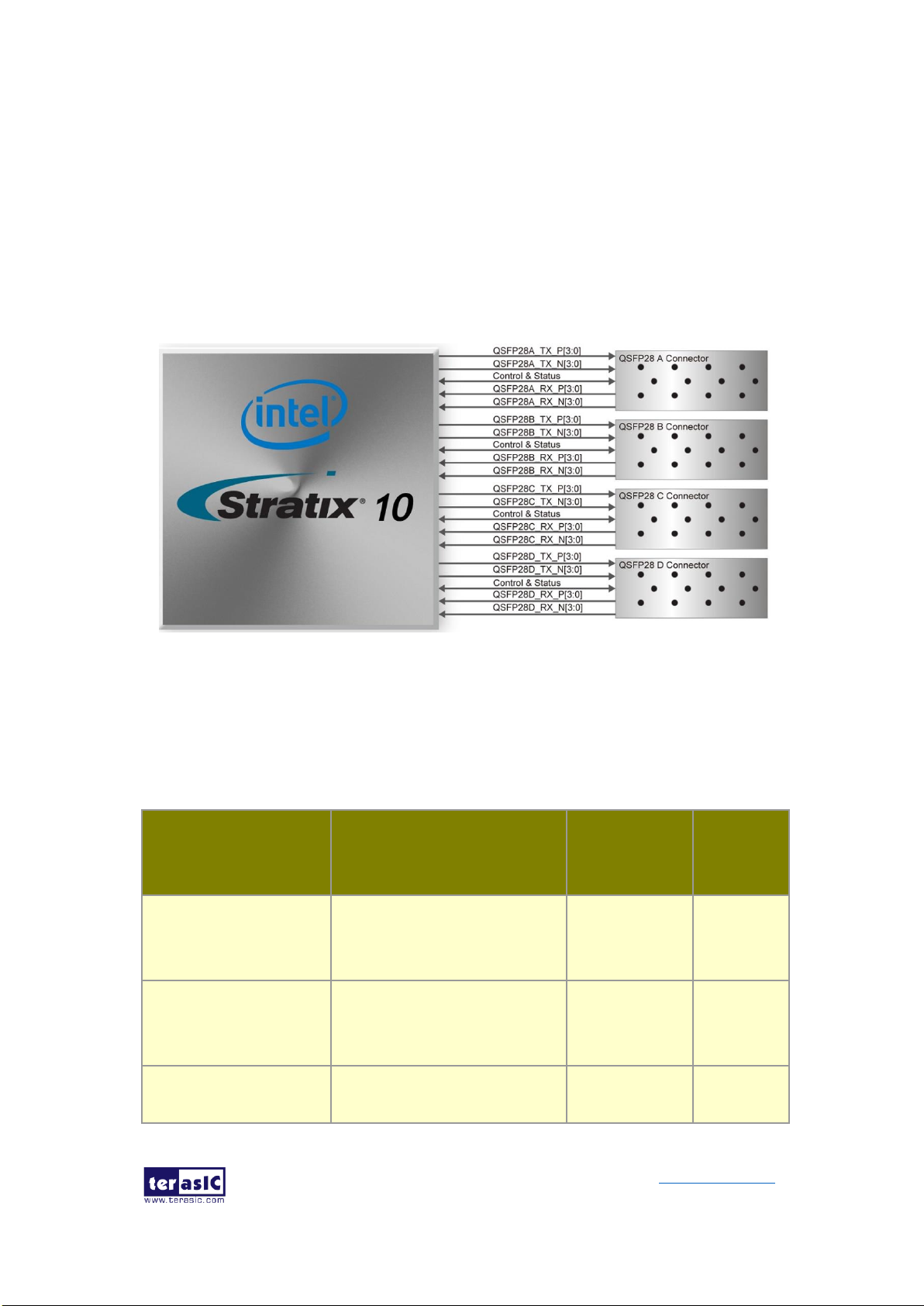
DE10-Pro
User Manual
51
www.terasic.com
September 24,
2019
2.9 QSPF28 Ports
The development board has four independent 100G QSFP28 connectors that use one
transceiver channel each from the Stratix 10 GX/SX FPGA device. These modules
take in serial data from the Stratix 10 GX/SX FPGA device and transform them to
optical signals. The board includes cage assemblies for the QSFP+ connectors.
Figure 2-15 shows the connections between the QSFP28 and Stratix 10 GX/SX
FPGA.
Figure 2-15 Connection between the QSFP28 and Stratix 10 GX/SX FPGA
Table 2-16, Table 2-17, Table 2-18 and Table 2-19 list the QSFP28 A, B, C and D pin
assignments and signal names relative to the Stratix 10 GX/SX device.
Table 2-16 QSFP28 A Pin Assignments, Schematic Signal Names, and Functions
Schematic
Signal Name
Description
I/O Standard
Stratix 10
GX/SX Pin
Number
QSFP28A_TX_P0
Transmitter data of channel 0
HSSI
DIFFERENTIAL
I/O
PIN_F49
QSFP28A_TX_N0
Transmitter data of channel 0
HSSI
DIFFERENTIAL
I/O
PIN_F48
QSFP28A_RX_P0
Receiver data of channel 0
HSSI
DIFFERENTIAL
PIN_G43

DE10-Pro
User Manual
52
www.terasic.com
September 24,
2019
I/O
QSFP28A_RX_N0
Receiver data of channel 0
HSSI
DIFFERENTIAL
I/O
PIN_G42
QSFP28A_TX_P1
Transmitter data of channel 1
HSSI
DIFFERENTIAL
I/O
PIN_G47
QSFP28A_TX_N1
Transmitter data of channel 1
HSSI
DIFFERENTIAL
I/O
PIN_G46
QSFP28A_RX_P1
Receiver data of channel 1
HSSI
DIFFERENTIAL
I/O
PIN_D45
QSFP28A_RX_N1
Receiver data of channel 1
HSSI
DIFFERENTIAL
I/O
PIN_D44
QSFP28A_TX_P2
Transmitter data of channel 2
HSSI
DIFFERENTIAL
I/O
PIN_E47
QSFP28A_TX_N2
Transmitter data of channel 2
HSSI
DIFFERENTIAL
I/O
PIN_E46
QSFP28A_RX_P2
Receiver data of channel 2
HSSI
DIFFERENTIAL
I/O
PIN_C43
QSFP28A_RX_N2
Receiver data of channel 2
HSSI
DIFFERENTIAL
I/O
PIN_C42
QSFP28A_TX_P3
Transmitter data of channel 3
HSSI
DIFFERENTIAL
I/O
PIN_C47
QSFP28A_TX_N3
Transmitter data of channel 3
HSSI
DIFFERENTIAL
I/O
PIN_C46
QSFP28A_RX_P3
Receiver data of channel 3
HSSI
DIFFERENTIAL
PIN_A43

DE10-Pro
User Manual
53
www.terasic.com
September 24,
2019
I/O
QSFP28A_RX_N3
Receiver data of channel 3
HSSI
DIFFERENTIAL
I/O
PIN_A42
QSFP28A_REFCLK_p
QSFP28A transceiver
reference clock p
LVDS
PIN_T41
QSFP28A_REFCLK_n
QSFP28A transceiver
reference clock n
LVDS
PIN_T40
QSFP28A_MOD_SEL_n
Module Select
3.0-V LVTTL
PIN_AD35
QSFP28A_RST_n
Module Reset
3.0-V LVTTL
PIN_AC33
QSFP28A_SCL
2-wire serial interface clock
3.0-V LVTTL
PIN_AC36
QSFP28A_SDA
2-wire serial interface data
3.0-V LVTTL
PIN_AC35
QSFP28A_LP_MODE
Low Power Mode
3.0-V LVTTL
PIN_AB36
QSFP28A_INTERRUPT
_n
Interrupt
3.0-V LVTTL
PIN_AB35
QSFP28A_MOD_PRS_
n
Module Present
3.0-V LVTTL
PIN_AB34
Table 2-17 QSFP28 B Pin Assignments, Schematic Signal Names, and Functions
Schematic
Signal Name
Description
I/O Standard
Stratix 10
GX/SX Pin
Number
QSFP28B_TX_P0
Transmitter data of channel 0
HSSI
DIFFERENTIAL
I/O
PIN_AK49
QSFP28B_TX_N0
Transmitter data of channel 0
HSSI
DIFFERENTIAL
I/O
PIN_AK48
QSFP28B_RX_P0
Receiver data of channel 0
HSSI
DIFFERENTIAL
I/O
PIN_AL43
QSFP28B_RX_N0
Receiver data of channel 0
HSSI
DIFFERENTIAL
I/O
PIN_AL42
QSFP28B_TX_P1
Transmitter data of channel 1
HSSI
DIFFERENTIAL
PIN_AL47

DE10-Pro
User Manual
54
www.terasic.com
September 24,
2019
I/O
QSFP28B_TX_N1
Transmitter data of channel 1
HSSI
DIFFERENTIAL
I/O
PIN_AL46
QSFP28B_RX_P1
Receiver data of channel 1
HSSI
DIFFERENTIAL
I/O
PIN_AH45
QSFP28B_RX_N1
Receiver data of channel 1
HSSI
DIFFERENTIAL
I/O
PIN_AH44
QSFP28B_TX_P2
Transmitter data of channel 2
HSSI
DIFFERENTIAL
I/O
PIN_AJ47
QSFP28B_TX_N2
Transmitter data of channel 2
HSSI
DIFFERENTIAL
I/O
PIN_AJ46
QSFP28B_RX_P2
Receiver data of channel 2
HSSI
DIFFERENTIAL
I/O
PIN_AF45
QSFP28B_RX_N2
Receiver data of channel 2
HSSI
DIFFERENTIAL
I/O
PIN_AF44
QSFP28B_TX_P3
Transmitter data of channel 3
HSSI
DIFFERENTIAL
I/O
PIN_AF49
QSFP28B_TX_N3
Transmitter data of channel 3
HSSI
DIFFERENTIAL
I/O
PIN_AF48
QSFP28B_RX_P3
Receiver data of channel 3
HSSI
DIFFERENTIAL
I/O
PIN_AG43
QSFP28B_RX_N3
Receiver data of channel 3
HSSI
DIFFERENTIAL
I/O
PIN_AG42
QSFP28B_REFCLK_p
QSFP28B transceiver
reference clock p
LVDS
PIN_AM38
DE10-Pro
User Manual
55
www.terasic.com
September 24,
2019
QSFP28B_REFCLK_n
QSFP28B transceiver
reference clock n
LVDS
PIN_AM37
QSFP28B_MOD_SEL_n
Module Select
3.0-V LVTTL
PIN_AJ33
QSFP28B_RST_n
Module Reset
3.0-V LVTTL
PIN_AG34
QSFP28B_SCL
2-wire serial interface clock
3.0-V LVTTL
PIN_AH32
QSFP28B_SDA
2-wire serial interface data
3.0-V LVTTL
PIN_AE36
QSFP28B_LP_MODE
Low Power Mode
3.0-V LVTTL
PIN_AF34
QSFP28B_INTERRUPT_n
Interrupt
3.0-V LVTTL
PIN_AF17
QSFP28B_MOD_PRS_n
Module Present
3.0-V LVTTL
PIN_AH17
Table 2-18 QSFP28 C Pin Assignments, Schematic Signal Names, and Functions
Schematic
Signal Name
Description
I/O Standard
Stratix 10
GX/SX Pin
Number
QSFP28C_TX_P0
Transmitter data of channel 0
HSSI
DIFFERENTIAL
I/O
PIN_AK1
QSFP28C_TX_N0
Transmitter data of channel 0
HSSI
DIFFERENTIAL
I/O
PIN_AK2
QSFP28C_RX_P0
Receiver data of channel 0
HSSI
DIFFERENTIAL
I/O
PIN_AL7
QSFP28C_RX_N0
Receiver data of channel 0
HSSI
DIFFERENTIAL
I/O
PIN_AL8
QSFP28C_TX_P1
Transmitter data of channel 1
HSSI
DIFFERENTIAL
I/O
PIN_AL3
QSFP28C_TX_N1
Transmitter data of channel 1
HSSI
DIFFERENTIAL
I/O
PIN_AL4
QSFP28C_RX_P1
Receiver data of channel 1
HSSI
DIFFERENTIAL
I/O
PIN_AH5
QSFP28C_RX_N1
Receiver data of channel 1
HSSI
PIN_AH6

DE10-Pro
User Manual
56
www.terasic.com
September 24,
2019
DIFFERENTIAL
I/O
QSFP28C_TX_P2
Transmitter data of channel 2
HSSI
DIFFERENTIAL
I/O
PIN_AJ3
QSFP28C_TX_N2
Transmitter data of channel 2
HSSI
DIFFERENTIAL
I/O
PIN_AJ4
QSFP28C_RX_P2
Receiver data of channel 2
HSSI
DIFFERENTIAL
I/O
PIN_AF5
QSFP28C_RX_N2
Receiver data of channel 2
HSSI
DIFFERENTIAL
I/O
PIN_AF6
QSFP28C_TX_P3
Transmitter data of channel 3
HSSI
DIFFERENTIAL
I/O
PIN_AF1
QSFP28C_TX_N3
Transmitter data of channel 3
HSSI
DIFFERENTIAL
I/O
PIN_AF2
QSFP28C_RX_P3
Receiver data of channel 3
HSSI
DIFFERENTIAL
I/O
PIN_AG7
QSFP28C_RX_N3
Receiver data of channel 3
HSSI
DIFFERENTIAL
I/O
PIN_AG8
QSFP28C_REFCLK_p
QSFP28C transceiver
reference clock p
LVDS
PIN_AM12
QSFP28C_REFCLK_n
QSFP28C transceiver
reference clock n
LVDS
PIN_AM13
QSFP28C_MOD_SEL_n
Module Select
3.0-V LVTTL
PIN_AE14
QSFP28C_RST_n
Module Reset
3.0-V LVTTL
PIN_AD15
QSFP28C_SCL
2-wire serial interface clock
3.0-V LVTTL
PIN_AD16
QSFP28C_SDA
2-wire serial interface data
3.0-V LVTTL
PIN_AF15
QSFP28C_LP_MODE
Low Power Mode
3.0-V LVTTL
PIN_AE16
QSFP28C_INTERRUPT_n
Interrupt
3.0-V LVTTL
PIN_AF16

DE10-Pro
User Manual
57
www.terasic.com
September 24,
2019
QSFP28C_MOD_PRS_n
Module Present
3.0-V LVTTL
PIN_AH16
Table 2-19 QSFP+ D Pin Assignments, Schematic Signal Names, and Functions
Schematic
Signal Name
Description
I/O Standard
Stratix 10
GX/SX
Pin
Number
QSFP28D_TX_P0
Transmitter data of channel 0
HSSI
DIFFERENTIAL
I/O
PIN_F1
QSFP28D_TX_N0
Transmitter data of channel 0
HSSI
DIFFERENTIAL
I/O
PIN_F2
QSFP28D_RX_P0
Receiver data of channel 0
HSSI
DIFFERENTIAL
I/O
PIN_G7
QSFP28D_RX_N0
Receiver data of channel 0
HSSI
DIFFERENTIAL
I/O
PIN_G8
QSFP28D_TX_P1
Transmitter data of channel 1
HSSI
DIFFERENTIAL
I/O
PIN_G3
QSFP28D_TX_N1
Transmitter data of channel 1
HSSI
DIFFERENTIAL
I/O
PIN_G4
QSFP28D_RX_P1
Receiver data of channel 1
HSSI
DIFFERENTIAL
I/O
PIN_D5
QSFP28D_RX_N1
Receiver data of channel 1
HSSI
DIFFERENTIAL
I/O
PIN_D6
QSFP28D_TX_P2
Transmitter data of channel 2
HSSI
DIFFERENTIAL
I/O
PIN_E3
QSFP28D_TX_N2
Transmitter data of channel 2
HSSI
DIFFERENTIAL
PIN_E4

DE10-Pro
User Manual
58
www.terasic.com
September 24,
2019
I/O
QSFP28D_RX_P2
Receiver data of channel 2
HSSI
DIFFERENTIAL
I/O
PIN_C7
QSFP28D_RX_N2
Receiver data of channel 2
HSSI
DIFFERENTIAL
I/O
PIN_C8
QSFP28D_TX_P3
Transmitter data of channel 3
HSSI
DIFFERENTIAL
I/O
PIN_C3
QSFP28D_TX_N3
Transmitter data of channel 3
HSSI
DIFFERENTIAL
I/O
PIN_C4
QSFP28D_RX_P3
Receiver data of channel 3
HSSI
DIFFERENTIAL
I/O
PIN_A7
QSFP28D_RX_N3
Receiver data of channel 3
HSSI
DIFFERENTIAL
I/O
PIN_A8
QSFP28D_REFCLK_p
QSFP28D transceiver
reference clock p
LVDS
PIN_T9
QSFP28D_REFCLK_n
QSFP28D transceiver
reference clock n
LVDS
PIN_T10
QSFP28D_MOD_SEL_n
Module Select
3.0-V LVTTL
PIN_AB12
QSFP28D_RST_n
Module Reset
3.0-V LVTTL
PIN_AB13
QSFP28D_SCL
2-wire serial interface clock
3.0-V LVTTL
PIN_AB14
QSFP28D_SDA
2-wire serial interface data
3.0-V LVTTL
PIN_AC14
QSFP28D_LP_MODE
Low Power Mode
3.0-V LVTTL
PIN_AB15
QSFP28D_INTERRUPT_n
Interrupt
3.0-V LVTTL
PIN_AD14
QSFP28D_MOD_PRS_n
Module Present
3.0-V LVTTL
PIN_AC15
2.10 PCI Express
The FPGA development board is designed to fit entirely into a PC motherboard with
x16 PCI Express slot. Utilizing built-in transceivers on a Stratix 10 GX/SX device, it is

DE10-Pro
User Manual
59
www.terasic.com
September 24,
2019
able to provide a fully integrated PCI Express-compliant solution for multi-lane (x1, x4,
x8 and x16) applications. With the PCI Express hard IP block incorporated in the
Stratix 10 GX/SX device, it will allow users to implement simple and fast protocol, as
well as saving logic resources for logic application. Figure 2-16 presents the pin
connection established between the Stratix 10 GX/SX and PCI Express.
The PCI Express interface supports complete PCI Express Gen1 at 2.5Gbps/lane,
Gen2 at 5.0Gbps/lane, and Gen3 at 8.0Gbps/lane protocol stack solution compliant to
PCI Express base specification 3.0 that includes PHY-MAC, Data Link, and transaction
layer circuitry embedded in PCI Express hard IP blocks.
Please note that it is a requirement that you connect the PCIe external power
connector 8-pin 12V DC power connector in the FPGA to avoid FPGA damage due to
insufficient power. The PCIE_REFCLK_p signal is a differential input that is driven from
the PC motherboard on this board through the PCIe edge connector. A DIP switch
(SW6) is connected to the PCI Express to allow different configurations to enable a x1,
x4, x8 or x16 PCIe.
Table 2-20 summarizes the PCI Express pin assignments of the signal names relative
to the Stratix 10 GX/SX FPGA.
Figure 2-16 PCI Express pin connection
Table 2-20 PCI Express Pin Assignments, Schematic Signal Names, and
Functions
Schematic
Signal Name
Description
I/O Standard
Stratix 10
GX/SX Pin
DE10-Pro
User Manual
60
www.terasic.com
September 24,
2019
Number
PCIE_TX_p0
Add-in card transmit bus
HIGH SPEED
DIFFERENTIAL
I/O
PIN_BJ46
PCIE_TX_n0
Add-in card transmit bus
HIGH SPEED
DIFFERENTIAL
I/O
PIN_BJ45
PCIE_TX_p1
Add-in card transmit bus
HIGH SPEED
DIFFERENTIAL
I/O
PIN_BF45
PCIE_TX_n1
Add-in card transmit bus
HIGH SPEED
DIFFERENTIAL
I/O
PIN_BF44
PCIE_TX_p2
Add-in card transmit bus
HIGH SPEED
DIFFERENTIAL
I/O
PIN_BG47
PCIE_TX_n2
Add-in card transmit bus
HIGH SPEED
DIFFERENTIAL
I/O
PIN_BG46
PCIE_TX_p3
Add-in card transmit bus
HIGH SPEED
DIFFERENTIAL
I/O
PIN_BE47
PCIE_TX_n3
Add-in card transmit bus
HIGH SPEED
DIFFERENTIAL
I/O
PIN_BE46
PCIE_TX_p4
Add-in card transmit bus
HIGH SPEED
DIFFERENTIAL
I/O
PIN_BF49
PCIE_TX_n4
Add-in card transmit bus
HIGH SPEED
DIFFERENTIAL
I/O
PIN_BF48
PCIE_TX_p5
Add-in card transmit bus
HIGH SPEED
DIFFERENTIAL
I/O
PIN_BC47
PCIE_TX_n5
Add-in card transmit bus
HIGH SPEED
DIFFERENTIAL
PIN_BC46
DE10-Pro
User Manual
61
www.terasic.com
September 24,
2019
I/O
PCIE_TX_p6
Add-in card transmit bus
HIGH SPEED
DIFFERENTIAL
I/O
PIN_BD49
PCIE_TX_n6
Add-in card transmit bus
HIGH SPEED
DIFFERENTIAL
I/O
PIN_BD48
PCIE_TX_p7
Add-in card transmit bus
HIGH SPEED
DIFFERENTIAL
I/O
PIN_BA47
PCIE_TX_n7
Add-in card transmit bus
HIGH SPEED
DIFFERENTIAL
I/O
PIN_BA46
PCIE_TX_p8
Add-in card transmit bus
HIGH SPEED
DIFFERENTIAL
I/O
PIN_BB49
PCIE_TX_n8
Add-in card transmit bus
HIGH SPEED
DIFFERENTIAL
I/O
PIN_BB48
PCIE_TX_p9
Add-in card transmit bus
HIGH SPEED
DIFFERENTIAL
I/O
PIN_AW47
PCIE_TX_n9
Add-in card transmit bus
HIGH SPEED
DIFFERENTIAL
I/O
PIN_AW46
PCIE_TX_p10
Add-in card transmit bus
HIGH SPEED
DIFFERENTIAL
I/O
PIN_AY49
PCIE_TX_n10
Add-in card transmit bus
HIGH SPEED
DIFFERENTIAL
I/O
PIN_AY48
PCIE_TX_p11
Add-in card transmit bus
HIGH SPEED
DIFFERENTIAL
I/O
PIN_AU47
PCIE_TX_n11
Add-in card transmit bus
HIGH SPEED
DIFFERENTIAL
PIN_AU46

DE10-Pro
User Manual
62
www.terasic.com
September 24,
2019
I/O
PCIE_TX_p12
Add-in card transmit bus
HIGH SPEED
DIFFERENTIAL
I/O
PIN_AV49
PCIE_TX_n12
Add-in card transmit bus
HIGH SPEED
DIFFERENTIAL
I/O
PIN_AV48
PCIE_TX_p13
Add-in card transmit bus
HIGH SPEED
DIFFERENTIAL
I/O
PIN_AR47
PCIE_TX_n13
Add-in card transmit bus
HIGH SPEED
DIFFERENTIAL
I/O
PIN_AR46
PCIE_TX_p14
Add-in card transmit bus
HIGH SPEED
DIFFERENTIAL
I/O
PIN_AT49
PCIE_TX_n14
Add-in card transmit bus
HIGH SPEED
DIFFERENTIAL
I/O
PIN_AT48
PCIE_TX_p15
Add-in card transmit bus
HIGH SPEED
DIFFERENTIAL
I/O
PIN_AP49
PCIE_TX_n15
Add-in card transmit bus
HIGH SPEED
DIFFERENTIAL
I/O
PIN_AP48
PCIE_RX_p0
Add-in card receive bus
CURRENT
MODE LOGIC
(CML)
PIN_BH41
PCIE_RX_n0
Add-in card receive bus
CURRENT
MODE LOGIC
(CML)
PIN_BH40
PCIE_RX_p1
Add-in card receive bus
CURRENT
MODE LOGIC
(CML)
PIN_BJ43
PCIE_RX_n1
Add-in card receive bus
CURRENT
MODE LOGIC
PIN_BJ42

DE10-Pro
User Manual
63
www.terasic.com
September 24,
2019
(CML)
PCIE_RX_p2
Add-in card receive bus
CURRENT
MODE LOGIC
(CML)
PIN_BG43
PCIE_RX_n2
Add-in card receive bus
CURRENT
MODE LOGIC
(CML)
PIN_ BG42
PCIE_RX_p3
Add-in card receive bus
CURRENT
MODE LOGIC
(CML)
PIN_BE43
PCIE_RX_n3
Add-in card receive bus
CURRENT
MODE LOGIC
(CML)
PIN_BE42
PCIE_RX_p4
Add-in card receive bus
CURRENT
MODE LOGIC
(CML)
PIN_BC43
PCIE_RX_n4
Add-in card receive bus
CURRENT
MODE LOGIC
(CML)
PIN_BC42
PCIE_RX_p5
Add-in card receive bus
CURRENT
MODE LOGIC
(CML)
PIN_BD45
PCIE_RX_n5
Add-in card receive bus
CURRENT
MODE LOGIC
(CML)
PIN_BD44
PCIE_RX_p6
Add-in card receive bus
CURRENT
MODE LOGIC
(CML)
PIN_BA43
PCIE_RX_n6
Add-in card receive bus
CURRENT
MODE LOGIC
(CML)
PIN_BA42
PCIE_RX_p7
Add-in card receive bus
CURRENT
MODE LOGIC
(CML)
PIN_BB45
PCIE_RX_n7
Add-in card receive bus
CURRENT
MODE LOGIC
PIN_BB44

DE10-Pro
User Manual
64
www.terasic.com
September 24,
2019
(CML)
PCIE_RX_p8
Add-in card receive bus
CURRENT
MODE LOGIC
(CML)
PIN_AW43
PCIE_RX_n8
Add-in card receive bus
CURRENT
MODE LOGIC
(CML)
PIN_AW42
PCIE_RX_p9
Add-in card receive bus
CURRENT
MODE LOGIC
(CML)
PIN_AY45
PCIE_RX_n9
Add-in card receive bus
CURRENT
MODE LOGIC
(CML)
PIN_AY44
PCIE_RX_p10
Add-in card receive bus
CURRENT
MODE LOGIC
(CML)
PIN_AU43
PCIE_RX_n10
Add-in card receive bus
CURRENT
MODE LOGIC
(CML)
PIN_AU42
PCIE_RX_p11
Add-in card receive bus
CURRENT
MODE LOGIC
(CML)
PIN_AV45
PCIE_RX_n11
Add-in card receive bus
CURRENT
MODE LOGIC
(CML)
PIN_AV44
PCIE_RX_p12
Add-in card receive bus
CURRENT
MODE LOGIC
(CML)
PIN_AR43
PCIE_RX_n12
Add-in card receive bus
CURRENT
MODE LOGIC
(CML)
PIN_AR42
PCIE_RX_p13
Add-in card receive bus
CURRENT
MODE LOGIC
(CML)
PIN_AT45
PCIE_RX_n13
Add-in card receive bus
CURRENT
MODE LOGIC
PIN_AT44

DE10-Pro
User Manual
65
www.terasic.com
September 24,
2019
(CML)
PCIE_RX_p14
Add-in card receive bus
CURRENT
MODE LOGIC
(CML)
PIN_AP45
PCIE_RX_n14
Add-in card receive bus
CURRENT
MODE LOGIC
(CML)
PIN_AP44
PCIE_RX_p15
Add-in card receive bus
CURRENT
MODE LOGIC
(CML)
PIN_AN43
PCIE_RX_n15
Add-in card receive bus
CURRENT
MODE LOGIC
(CML)
PIN_AN42
PCIE_REFCLK_p
Motherboard reference clock
HCSL
PIN_AM41
PCIE_REFCLK_n
Motherboard reference clock
HCSL
PIN_AM40
PCIE_PERST_n
Reset
3.0-V LVTTL
PIN_AJ34
PCIE_SMBCLK
SMB clock
1.2-V
PIN_BA39
PCIE_SMBDAT
SMB data
1.2-V
PIN_BF40
PCIE_WAKE_n
Wake signal
1.2-V
PIN_BC33
PCIE_PRSNT1n
Hot plug detect
-
-
PCIE_PRSNT2n_x1
Hot plug detect x1 PCIe slot
enabled using SW6 dip switch
-
-
PCIE_PRSNT2n_x4
Hot plug detect x4 PCIe slot
enabled using SW6 dip switch
-
-
PCIE_PRSNT2n_x8
Hot plug detect x8 PCIe slot
enabled using SW6 dip switch
-
-
PCIE_PRSNT2n_x16
Hot plug detect x16 PCIe slot
enabled using SW6 dip switch
-
-

DE10-Pro
User Manual
66
www.terasic.com
September 24,
2019
Chapter 3
System Builder
his chapter describes how users can create a custom design project for the
FPGA board from a software tool named System Builder.
3.1 Introduction
The System Builder is a Windows based software utility. It is designed to help users
create a Quartus Prime project for the FPGA board within minutes. The Quartus Prime
project files generated include:
⚫ Quartus Prime Project File (.qpf)
⚫ Quartus Prime Setting File (.qsf)
⚫ Top-Level Design File (.v)
⚫ External PLL Controller (.v)
⚫ Synopsis Design Constraints file (.sdc)
⚫ Pin Assignment Document (.htm)
The System Builder not only can generate the files above, but can also provide
error-checking rules to handle situation that are prone to errors. The common mistakes
that users encounter are the following:
⚫ Board damaged for wrong pin/bank voltage assignment.
⚫ Board malfunction caused by wrong device connections or missing pin
counts for connected ends.
⚫ Performance dropped because of improper pin assignments
T

DE10-Pro
User Manual
67
www.terasic.com
September 24,
2019
3.2 General Design Flow
This section will introduce the general design flow to build a project for the FPGA board
via the System Builder. The general design flow is illustrated in Figure 3-1.
Users should launch System Builder and create a new project according to their design
requirements. When users complete the settings, the System Builder will generate two
major files which include top-level design file (.v) and the Quartus Prime setting file
(.qsf).
The top-level design file contains top-level Verilog wrapper for users to add their own
design/logic. The Quartus Prime setting file contains information such as FPGA device
type, top-level pin assignment, and I/O standard for each user-defined I/O pin.
Finally, the Quartus Prime programmer must be used to download SOF file to the
FPGA board using JTAG interface.
Figure 3-1 the general design flow of building a project
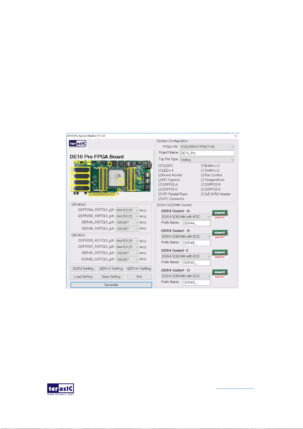
DE10-Pro
User Manual
68
www.terasic.com
September 24,
2019
3.3 Using System Builder
This section provides detailed procedures on how the System Builder is used.
◼ Install and Launch the System Builder
The System Builder is located under the directory: "Tools\SystemBuilder" in the
System CD. Users can copy the entire folder to the host computer without installing the
utility. Please execute the SystemBuilder.exe on the host computer, as shown in
Figure 3-2.
Figure 3-2 The System Builder window
◼ Select FPGA
As described in section 1.2, DE10-Pro version B supports three types FPGA, users
can select FPGA P/N in System Builder as shown in Figure 3-3.
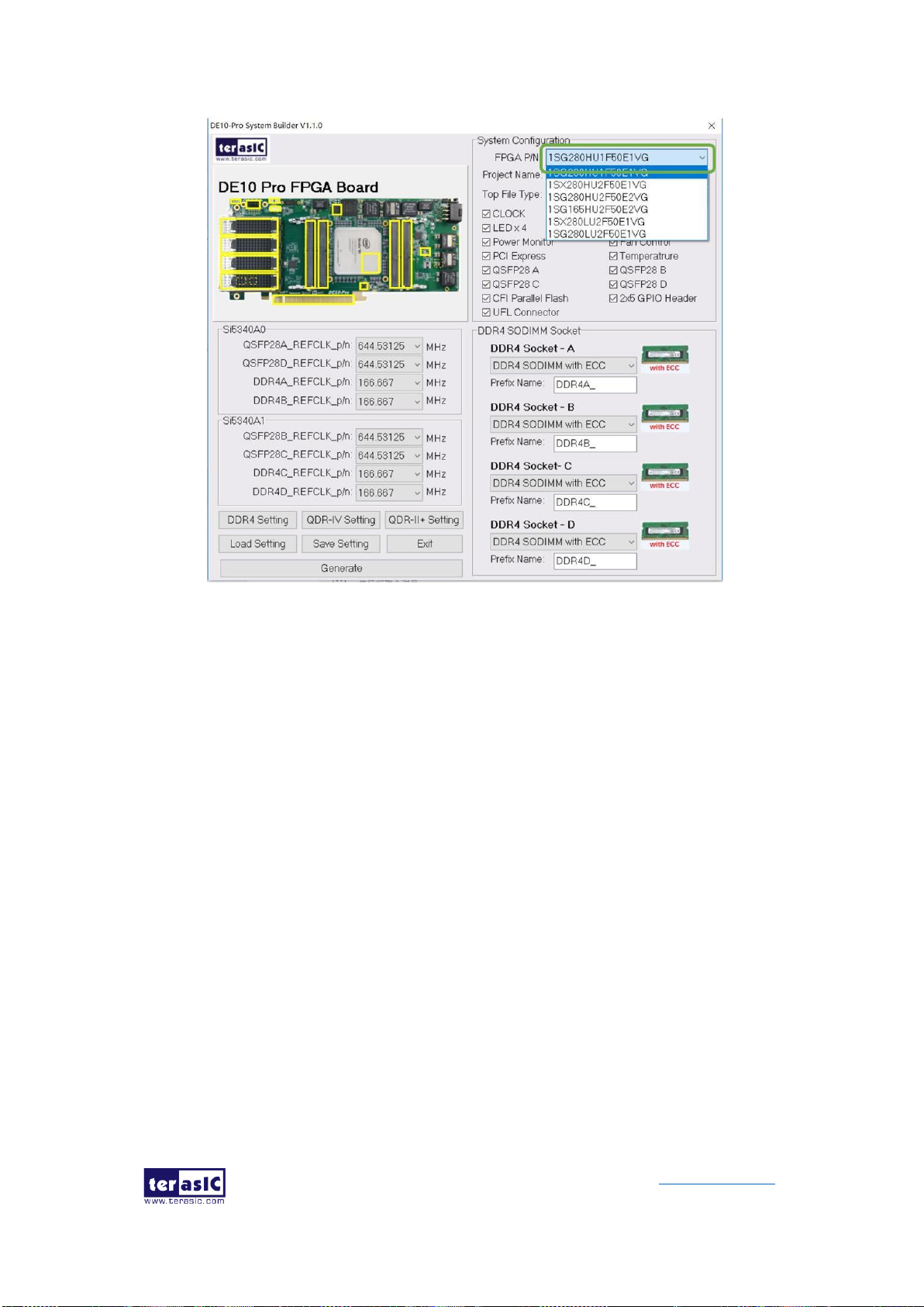
DE10-Pro
User Manual
69
www.terasic.com
September 24,
2019
Figure 3-3 Select FPGA
◼ Enter Project Name
The project name entered in the circled area as shown in Figure 3-4, will be assigned
automatically as the name of the top-level design entry.

DE10-Pro
User Manual
70
www.terasic.com
September 24,
2019
Figure 3-4 Project Name in the System Builder window
◼ Select Top File Type
The system builder can generate Verilog or VHDL Quartus top file according to the
users’ requirements. Users can select their desired file type in the Top File Type list-box
shown in Figure 3-5.

DE10-Pro
User Manual
71
www.terasic.com
September 24,
2019
Figure 3-5 Top File Type in the System Builder window
◼ System Configuration
Users are given the flexibility of enabling their choices of components connected to the
FPGA under System Configuration, as shown in Figure 3-6. Each component of the
FPGA board is listed to be enabled or disabled according to users’ needs. If a
component is enabled, the System Builder will automatically generate the associated
pin assignments including its pin name, pin location, pin direction, and I/O standards.
Note: The pin assignments for some components (e.g. DDR4 and QSFP28) require
associated controller codes in the Quartus project or it would result in compilation error.
Hence please do not select them if they are not needed in the design. To use the DDR4
controller, please refer to the DDR4 SDRAM demonstration in Chapter 6.

DE10-Pro
User Manual
72
www.terasic.com
September 24,
2019
Figure 3-6 System Configuration Group
◼ Programmable Clock Generator
There are two external clock generator Si5340A on-board that provide reference clocks
for the following signals:
⚫ QSFP28A_REFCLK
⚫ QSFP28B_REFCLK
⚫ QSFP28C_REFCLK
⚫ QSFP28D_REFCLK
⚫ DDR4A_REFCLK
⚫ DDR4B_REFCLK
⚫ DDR4C_REFCLK
⚫ DDR4D_REFCLK
To use these clock, users can select the desired frequency on the Si5340A0 and
Si5340A1 groups, as shown in Figure 3-7. DDR4 or QSFP28 must be checked before
users can start to specify the desired frequency in the programmable oscillators.

DE10-Pro
User Manual
73
www.terasic.com
September 24,
2019
As the Quartus project is created, System Builder automatically generates the
associated controller according to users’ desired frequency in Verilog which facilitates
users’ implementation as no additional control code is required to configure the
programmable oscillator.
Note: If users need to dynamically change the frequency, they would need to modify
the generated control code themselves.
Figure 3-7 External programmable oscillators
◼ Project Setting Management
The System Builder also provides functions to restore default DDR4/QDR-II+/QDR-IV
setting, load a pre-saved setting, and save board configuration file, as shown in Figure
3-8. Users can save the current board configuration information into a .cfg file and load
it into the System Builder later.

DE10-Pro
User Manual
74
www.terasic.com
September 24,
2019
Figure 3-8 Project Settings
◼ Project Generation
When users press the Generate button, the System Builder will generate the
corresponding Quartus Prime files and documents as listed in the Table 3- directory
specified by the user.
Table 3-1 Files generated by the System Builder
No.
Filename
Description
1
<Project name>.v
or
<Project name>.vhdl
Top Level Verilog/VHDL File for Quartus Prime
2
si5340_controller (*)
Si5340A Clock Generator Controller IP
3
<Project name>.qpf
Quartus Prime Project File
4
<Project name>.qsf
Quartus Prime Setting File
5
<Project name>.sdc
Synopsis Design Constraints File for Quartus Prime
6
<Project name>.htm
Pin Assignment Document

DE10-Pro
User Manual
75
www.terasic.com
September 24,
2019
(*) The si5340_controller is a folder which contains the Verilog files for the
configuration of Si5340A clock generator chips.
Users can add custom logic into the project and compile the project in Quartus Prime
to generate the SRAM Object File (.sof).
The Si5340A controllers will be instantiated in the Quartus Prime top-level file, as listed
below:
The following clock information also be automatically added in .sdc file.
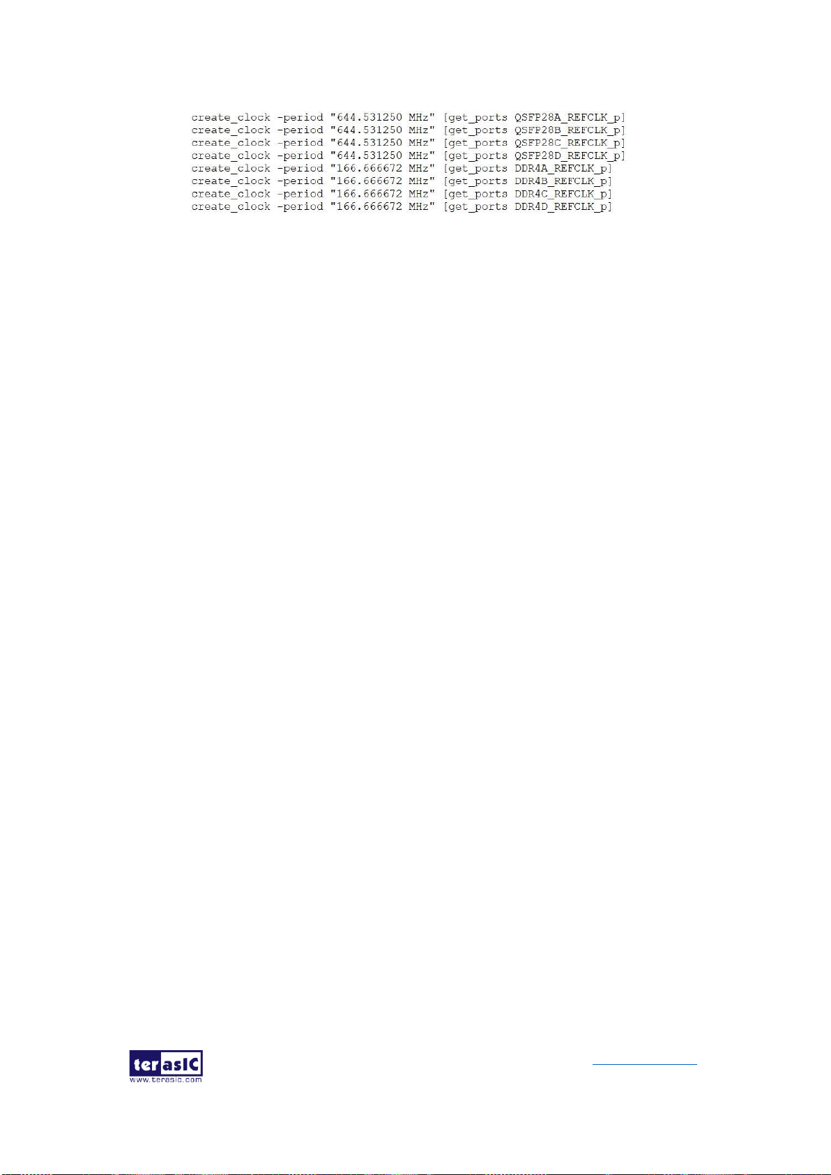
DE10-Pro
User Manual
76
www.terasic.com
September 24,
2019
If the dynamic configurations for the Si5340A clock generators are required, users
need to modify the code according to users’ desired behavior.

DE10-Pro
User Manual
77
www.terasic.com
September 24,
2019
Chapter 4
CFI-Flash Programming
s you develop your own project using the Altera tools, you can program the
flash memory device so that your own design loads from CFI flash memory
into the FPGA on power up. This chapter will describe how to use Altera
Quartus Prime Programmer Tool to program the common flash interface (CFI) flash
memory device on the FPGA board.
The Stratix 10 GX/SX FPGA development board ships with the CFI flash device
preprogrammed with two FPGA configurations. The two configuration images are
called: factory image and user image, respectively.
4.1 FPGA Configure Operation
Below shows the procedure to enable the FPGA configuration from Flash. Users can
select one boot image between factory image and user image.
1. Make sure the two default FPGA configurations data has been stored in the CFI
flash.
2. Set the FPGA configuration mode to AVSTx8 mode by setting SW5/4 MSEL[2:0]
as 110 as shown in Figure 4-1.
3. Specify the configuration of the FPGA using the default Factory Configuration
Image or User Configuration Image by setting SW4 according to Figure 4-2.
When the switch is in position “1”, the factory image is used when the system
boots. When the switch is in position “0”, user image is used when the system
boots.
4. Power on the FPGA board or press the MAX_RST button if board is already
powered on,
5. When the configuration is completed, the green Configure Done LED will light. If
there is an error, the red Configure Error LED will light.
A

DE10-Pro
User Manual
78
www.terasic.com
September 24,
2019
Figure 4-1 MSEL[2:0]=110
Figure 4-2 Configuration Image Selection
4.2 CFI Flash Memory Map
The DE10-Pro has one 1-Gbit, 16-bit data width, CFI compatible synchronous flash
device for non-volatile storage of the FPGA configuration data, user Nios II code, and
user data. Both MAX V CPLD and Stratix 10 GX/SX FPGA can access this Flash
device.
MAX V CPLD accesses are for AVST x8 configuration of the FPGA at power-on and
board reset events. It uses the PFL-II Mega function. Stratix 10 GX/SX FPGA access to
the flash memory's user space is done by Nios II.
Table 4-1 shows the memory map for the on-board flash. This memory provides

DE10-Pro
User Manual
79
www.terasic.com
September 24,
2019
non-volatile storage for two FPGA bit-streams and Nios II Program, users data, as well
as FPL option bits for PFL II configuration bits and board information. For the factory
default code to run correctly and update designs in the user memory, this memory map
address must not be altered.
Table 4-1 Flash Memory Map (Byte Address)
Block Description
Size(KB)
Address Range
Factory Board Information
128
0x00010000 – 0x0002FFFF
PFL option bits
64
0x00030000 – 0x0003FFFF
Factory hardware
57,856
0x00040000 – 0x038BFFFF
User hardware
57,856
0x038C0000 – 0x0713FFFF
Factory software
1,024
0x07140000 – 0x0723FFFF
User software and data
14,080
0x07240000 – 0x07FFFFFF
The Factory Board Information stores the Manufacture Serial Number of the FPGA
board. The Serial Number is a 13digital number with format mmmmmmmm-nnnn.
Users can find the number on the serial number sticker on the FPGA board.
The PFL option bits contains the image location of the Factory hardware and User
hardware, so the PLF II IP in the MAX can know where to find the FPGA configuration
data. If developers erase all flash content, please ensure that the PFL option is
reprogrammed with the FPGA configuration data.
For user’s application, the User hardware must be stored with start address
0x038C0000, and the user’s software is suggested to be stored with start address
0x07240000. Users also can overwrite the Factory hardware and Factory software
based on their application. Factory hardware must be stored with start address
0x00040000, and the Factory software should be stored with start address
0x07140000. We strongly recommend users to use the batch file in the
Flash_Restored folder to write the hardware and software data into the CFI-Flash.
4.3 Flash Example Designs
There are four flash example designs and one programming batch folder in the
Demonstration folder under the System CD as shown in Table 4-2.
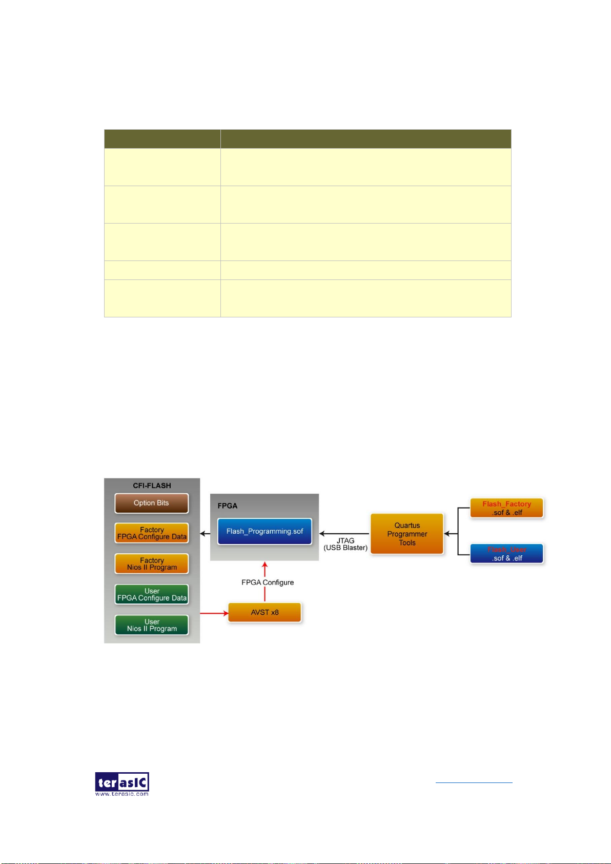
DE10-Pro
User Manual
80
www.terasic.com
September 24,
2019
Table 4-2 Flash Example Design
Example Folder
Description
Flash_Programming
This is the flash programming design. It is used to write
data into FLASH by a Quartus Programmer.
Flash_Factory
A simple example design. Its FPGA configure data and
Nios II codes are stored in the Factory Image Area.
Flash_User
A simple example design. Its FPGA configure data and
Nios II codes are stored in the User Image Area.
Flash_Tool
A Nios II program shows how to access flash content.
Flash_Restored
A batch file used for to programming Flash_Factory and
the Flash_User project into CFI Flash.
Figure 4-3 shows the relationship between the three examples –
Flash_Programming, Flash_Factory and Flash_User. The Flash_Programming
example is used to write data into the CFI Flash on the FPGA Board. The
Flash_Factory and Flash_User are simple designs with Nios II processor. These two
designed are written into CFI-Flash so they are selected to configure the FPGA when
the FPGA is powered on.
Figure 4-3 Relationship between three flash examples
The Flash_Tool is designed to show how to access flash via the Nios II processor. The
design shows how to erase flash and read flash content.

DE10-Pro
User Manual
81
www.terasic.com
September 24,
2019
4.4 Flash_Programming Example
The Flash_Programing project is designed to program CFI flash by a Quartus
Programmer. In the project, Intel Parallel Flash Loader II IP is used to program the
CFI-Flash. Figure 4-4 shows the Generic Setting in the IP. “Flash Programming”
operation mode is used, and “CFI Parallel Flash” is selected. Figure 4-5 shows the
Flash Interface Setting. “CFI 1 Gbit” is selected. The DE10-Pro.sof generated by this
program is used in the flash programming batch files located in the Flash_Restored
Folder.
Figure 4-4 General Setting in PFL II IP
Figure 4-5 Flash Interface Setting in PFL II IP
4.5 Flash_Factory Example
The Flash_Factory is designed to show how to create a Nios II code which is booted
from the Factory Software location in the CFI Flash when the board is powered on.
This project’s FPGA configuration data and Nios II code are stored in the Factory Hard
area and Factory Software area of the CFI Flash when the FPGA board is shipped.

DE10-Pro
User Manual
82
www.terasic.com
September 24,
2019
To develop this kind of boot code, first, developers need to include the Tri-State
Conduit Bridge and the Generic Tri-State Controller in the Platform Designer
(formerly Qsys) to implement the flash controller function, and connect the Nios II
processor’s data bus and instruction bus to the flash controller as shown in Figure 4-6 .
Then, specify the Factory Software Location 0x07140000 as Reset Vector in the Nios II
Processor component as shown in Figure 4-7. Finally, developers need to uncheck the
allow_code_at_reset and enable_alt_load options in the BSP editor under of Nios II
IDE tool (Nios II Software Builder Tools for Eclipse) as shown in Figure 4-8 .
Figure 4-6 Flash Controller Settings in Platform Designer (formerly Qsys)
Figure 4-7 Factory Software Reset Vector Settings for NIOS II Processor
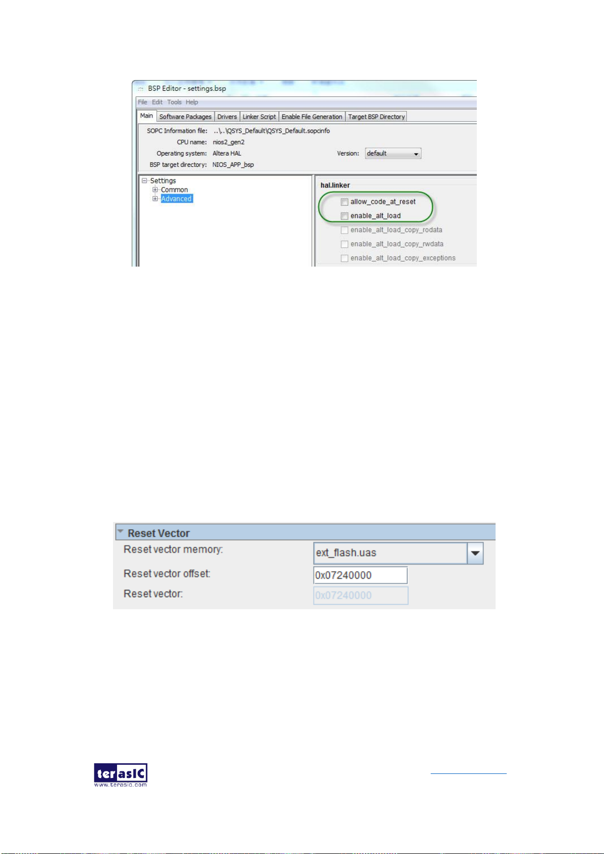
DE10-Pro
User Manual
83
www.terasic.com
September 24,
2019
Figure 4-8 BSP Editor in Nios II IDE
4.6 Flash_User Example
The Flash_User project is similar with the above Flash_Factory example code. This
project’s FPGA configuration data and Nios II code are stored in the User Hard area
and User Software area when the FPGA board is shipped.
The major difference between the Flash_User and Flash_Factory is the Reset Vector
address in the Nios II processor component and the LED control code in Nios II
program. The User Software Location 0x07240000 is used as Reset Vector as shown
in Figure 4-9.
Figure 4-9 User Software Reset Vector Settings for NIOS II Processor
4.7 Flash_Tool Example
This example show how the Nios II program accesses the FLASH. Figure 4-10 shows
a screenshot of the Flash_Tool menu shown under Nios II terminal.

DE10-Pro
User Manual
84
www.terasic.com
September 24,
2019
Figure 4-10 Screenshot of Flash_Tool menu
The tools provide the following functions:
⚫ Show CFI Flash Size
⚫ Show Option bits used by AVST x8 Configuration
⚫ Read Serial Number from the CFI Flash
⚫ Erase Serial Number to the CFI flash
⚫ Erase option bits used by AVST x8
⚫ Erase whole flash
4.8 Programming Batch File
The Flash_Restored folder includes batch files to program the Factory image and
User image into the CFI flash. Figure 4-11 shows the contents of the Flash_Restored
folder. The factory subfolder includes the .sof & .elf files generated by the
Flash_Factory project. The user subfolder includes the .sof & .elf files generated by
the Flash_User project. DE10_Pro.sof is generated by the Flash_Programming
project.
Figure 4-11 Flash_Restored folder content
The flash_program.bat is the top batch file for flash programming. The batch file will
configure the FPGA with DE10_Pro.sof (Parallel Flash Loader II IP) and launch
flash_program.sh Nios II command batch file to perform the following tasks:

DE10-Pro
User Manual
85
www.terasic.com
September 24,
2019
1. Use Nios II utilities elf2flash and nios2-elf-objcopy to convert Factory Nios II
code and User Nios II code to factory_sw.hex and user_sw.hex, respectively.
2. Use quartus_cpf utility according to a given configuration file flash.cof to merger
all files (factory_sw.hex, user_sw.hex, factory .sof file, user .sof file, and option bit)
into a single file flash.pof.
3. Use jtagconfig utility to adjust jtag speed.
4. Use quartus_pgm utility to program flash with flash.pof.
Developers can copy their .sof & .efl files into the factory folder or the user folder, and
launch the flash_program.bat to program their code into the CFI-Flash.
4.9 Restore Factory Settings
This section describes how to restore the original Factory image and User image into
the flash memory device on the FPGA development board. A programming batch file
located in the Flash_Restored folder is used to restore the flash content. Performing
the following instructions can restore the flash content:
1. Make sure the Nios II EDS and USB-Blaster II driver are installed.
2. Make sure the FPGA board and PC are connected with an USB Cable.
3. Power on the FPGA board.
4. Copy the “Demonstrations/Flash_Restored” folder under the CD to your PC’s
local drive.
5. Execute the batch file flash_program.bat to start flash programming.
After restoring the flash, perform the following procedures to test the restored boot
code.
1. Power off the FPGA Board.
2. Set FPGA configuration mode as AVSTx8 Mode by setting SW4/5 MSEL[2:0]
to 110.
3. Specify configuration of the FPGA to Factory Hardware by setting the
FACTORY_LOAD dip in SW4 to the ‘1’ position.
4. Power on the FPGA Board, and the Configure Done LED should light up.
The batch file converts the Factory and User .sof/.elf and PFL option bit into a
flash.pof file and use Quartus Programmer to program the CFI-Flash with the

DE10-Pro
User Manual
86
www.terasic.com
September 24,
2019
generated flash.pof. The factory subfolder includes DE10_Pro.sof and NIOS_APP.elf
files generated by Flash_Factory project, and the user subfolder includes
DE10_Pro.sof and HELLO_NIOS.elf files generated by Flash_User project. The
DE10_Pro.sof under the Flash_Restored folder is used to program flash by Quartus
Programmer.

DE10-Pro
User Manual
87
www.terasic.com
September 24,
2019
Chapter 5
Peripheral Reference
Design
his chapter introduces DE10-Pro peripheral interface reference designs. It
mainly introduces Si5340A chip which is a programmable clock generator. We
provide two ways (Pure RTL IP and Nios II System) respectively to show how
to control Si5340A to output desired frequencies, as well as how to control the fan
speed. The source codes and tools of these examples are all available in the System
CD.
5.1 Configure Si5340A in RTL
There are two Silicon Labs Si5340A clock generators on DE10-Pro FPGA board can
provide adjustable frequency reference clock (See Figure 5-1) for QSFP28 connectors
and memory modules (DDR4, QDR-II+, QDR-IV). Each Si5340A clock generator can
output four differential frequencies from 100Hz ~ 712.5Mhz though I2C interface
configuration. This chapter will show you how to use FPGA RTL IP to configure each
Si5340A PLL and generate users desired output frequency to each peripheral. In the
following instruction, the two Si5340A chips will be named as Si5340A0 and Si5340A1
respectively.
T

DE10-Pro
User Manual
88
www.terasic.com
September 24,
2019
Figure 5-1 The clock tree of the DE10-Pro
◼ Creating Si5340A Control IP
The Si5340A control IP is located in the folder: "\Demonstrations\si5340_control_ip" in
the System CD. Developers can use the IP directly in their Quartus top. Developers
can refer to the example in Demonstrations/Clock_Controller folder. This example
shows how to instantiate the IP in Quartus top project.
Also, System Builder tool (located in System CD) can be used to help developer to set
Si5340A to output desired frequencies, and generate a Quartus project with control IP.
In the System Builder window, users can select desired frequencies as shown in
Figure 5-2. Developers can click the “DDR4 Setting”, “QDR-IV Setting”, or “QDR-II+
setting” to user pre-setting output frequency for various memory modules. Then,
modify the output frequency by selecting a desired output frequency in the pull down
menu. For details about the System Builder, please refer to Chapter 3 – System
Builder.

DE10-Pro
User Manual
89
www.terasic.com
September 24,
2019
Figure 5-2 Select Desired Si5340A output frequency
◼ Using Si5340 control IP
Table 5-1 lists the instruction ports of Si5340A Controller IP.
Table 5-1 Si5340A Controller Instruction Ports
Port
Direction
Description
iCLK
input
System Clock (50Mhz)
iRST_n
input
Synchronous Reset
(0: Module Reset, 1: Normal)
iStart
input
Start to Configure(positive edge trigger)
iXCVR0_REFCLK
iXCVR1_REFCLK
iMEM0_REFCLK
iMEM1_REFCLK
input
Setting Si5340A Output Channel
Frequency Value
oPLL_REG_CONFIG_DONE
output
Si5340 Configuration status
( 0: Configuration in Progress, 1:
Configuration Complete)

DE10-Pro
User Manual
90
www.terasic.com
September 24,
2019
I2C_DATA
inout
I2C Serial Data to/fromSi5340A
I2C_CLK
output
I2C Serial Clock to Si5340A
As shown in Table 5-2 and Table 5-3, both two Si5340A control IPs have preset
several output frequency parameters, if users want to change frequency, users can fill
in the input ports " iXCVR0_REF_CLK", " iXCVR1_REF_CLK", " iMEM0_REF_CLK",
and " iMEM1_REF_CLK" with desired frequency values and recompile the project.
For example, in the components Si5340A0 and Si5340A1, change
.iXCVR0_REFCLK(`XCVR_REF_644M53125),
to
.iXCVR0_REFCLK(`XCVR_REF_322M265625),
Recompile project, the Si5340A0 OUT0 channel (for QSFP28D ) output frequency will
change from 644.53125Mhz to 322.26562Mhz.
Table 5-2 Si5340A Controller Reference Clock Frequency Setting for QSFP28
iXCVR0_REFCLK
iXCVR1_REFCLK
Input Setting
Si5340A Channel Clock Frequency(MHz)
4'h0
644.53125
4'h1
322.265625
4'h2
250
4'h3
125
4'h4
100
Table 5-3 Si5340A Controller Reference Clock Frequency Setting for Memory
iMEM0_REFCLK
iMEM1_REFCLK
Input Setting
Si5340A Channel Clock Frequency(MHz)
4'h0
300
4'h1
275
4'h2
266.667
4'h3
233.333
4'h4
166.667

DE10-Pro
User Manual
91
www.terasic.com
September 24,
2019
Users can also dynamically modify the input parameters, and input a positive edge
trigger for “iStart”, then, Si5340A output frequency can be modified.
After the manually modifying, please remember to modify the corresponding frequency
value in SDC file.
◼ Modify Clock Parameter for Your Own Frequency
If the Si5340A control IP built-in frequencies are not users’ desired, users can refer to
the below steps to the modify control IP register parameter settings to modify the IP to
output a desired frequency.
1. Firstly, download ClockBuilder Pro Software (See Figure 5-3), which is
provided by Silicon Labs. This tool can help users to set the Si5340A’s output
frequency of each channel through the GUI interface, and it will automatically
calculate the Register parameters required for each frequency. The tool
download link:
http://url.terasic.com/clockuilder_ro_oftware
Figure 5-3 ClockBuilder Pro Wizard
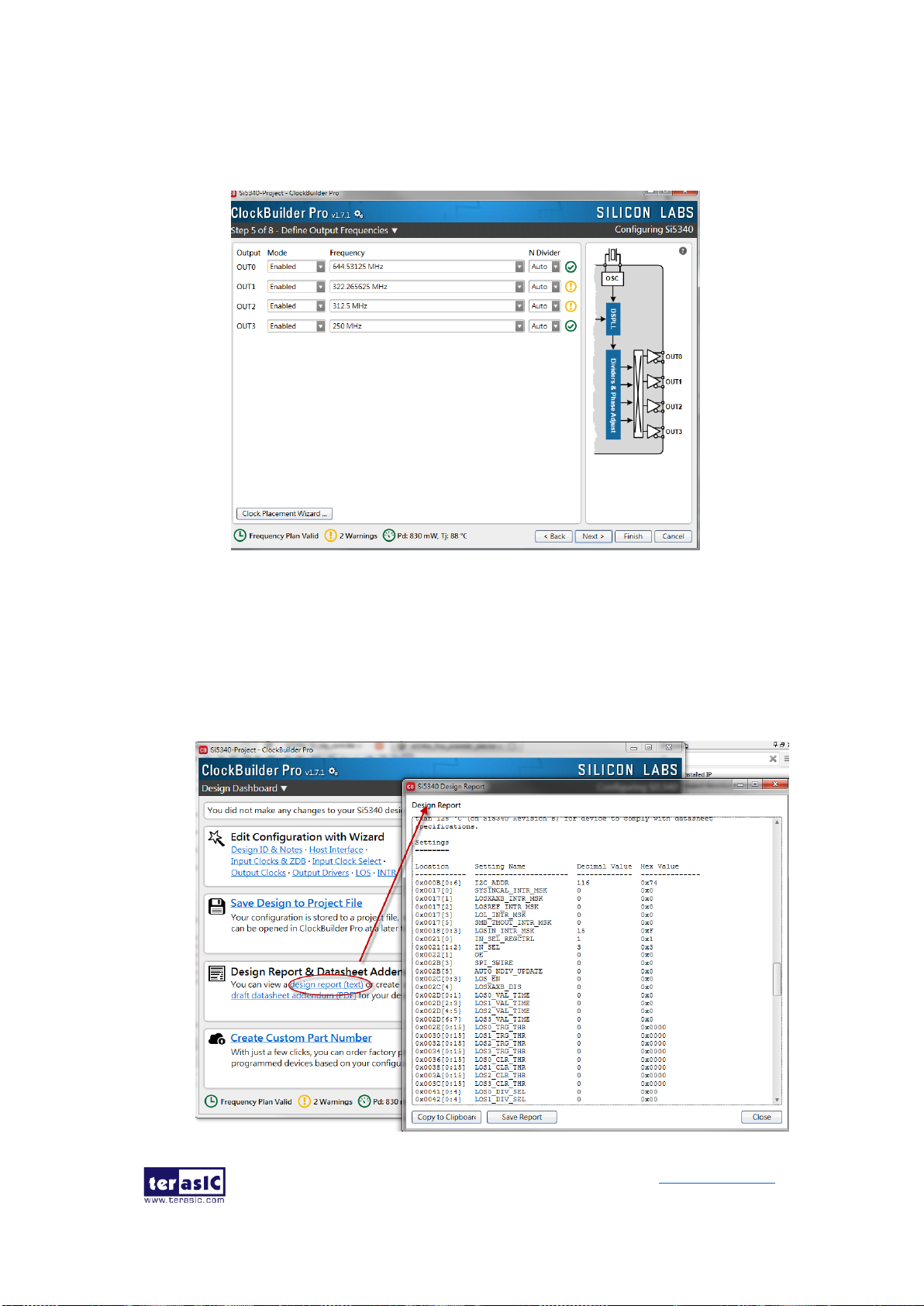
DE10-Pro
User Manual
92
www.terasic.com
September 24,
2019
2. After the installation, select Si5340, and configure the input frequency and
output frequency as shown in Figure 5-4.
Figure 5-4 Define Output Clock Frequencies on ClockBuilder Pro Wizard
3. After the setting is completed, ClockBuilder Pro Wizard generates a Design
Report(text), which contains users setting frequency corresponding register
value (See Figure 5-5).

DE10-Pro
User Manual
93
www.terasic.com
September 24,
2019
Figure 5-5 Open Design Report on ClockBuilder Pro Wizard
4. Open Si5340 control IP sub-module “si5340a_i2c_reg_controller.v “ as shown
in Figure 5-6, refer to Design Report parameter to modify sub-module
corresponding register value (See Figure 5-7).
Figure 5-6 Sub-Module file "si5340a_i2c_reg_controller.v"
Figure 5-7 Modify Si5340 Control IP Base on Design Report
After modifying and compiling, Si5340A can output new frequencies according to the
users’ setting.
Note :
1. No need to modify all Design Report parameters in
si5340a_i2c_reg_controller.v/si5340b_i2c_reg_controller.v, users can ignore

DE10-Pro
User Manual
94
www.terasic.com
September 24,
2019
parameters which have nothing to do with the frequency setting
2. After manually modifying, please remember to modify clock constrain setting
in .SDC file
5.2 Nios II control for SI5340/
Temperature/ Power/Fan
This demonstration shows how to use the Nios II processor to:
⚫ monitor system temperature with the on-board temperature sensor
⚫ program on-board two programmable oscillators (Si5340A0 and Si5340A1)
⚫ measure the power consumption based on the built-in power measure circuit
⚫ control fan speed and monitor rotation speed.
◼ System Block Diagram
Figure 5-8 shows the system block diagram of this demonstration. The system
requires a 50 MHz clock provided from the board. The six peripherals (including one
temperature sensor, two Si5340A clock generator, and two LTC2945 for 12V input
power monitor and FPGA core power monitor, and one fan controller chip MAX6651)
are all controlled through five I2C controllers driven by Nios II program. The Nios II
program is running in the on-chip memory.

DE10-Pro
User Manual
95
www.terasic.com
September 24,
2019
Figure 5-8 Block diagram of the Nios II Basic Demonstration
The program provides a menu in nios-terminal, as shown in Figure 5-9 to provide an
interactive interface. With the menu, users can perform the test for the temperature
sensors, external PLL and power monitor. Note, pressing ‘ENTER’ should be followed
with the user’s number of choice.
Figure 5-9 Menu of Demo Program
In temperature test, the program will display local temperature and remote temperature.
The remote temperature is the FPGA temperature, and the local temperature is the

DE10-Pro
User Manual
96
www.terasic.com
September 24,
2019
board temperature where the temperature sensor located.
There are two power monitor chips (LTC2945) embedded on the board to monitor in
real-time the input 12V power and 0.9V FPGA core power. The U55 LTC2945 is used
to monitor 12V input power with two sense resistors 0.003 ohm parallel. Its I2C device
address is 0xD4/D5. The U67 LTC2945 is used to monitor the 0.9V FPGA core power
with two sense resistors 0.00025 ohmin parallel. Its I2C device address is 0x0A/0x0B.
These two chips share the same I2C bus.
In the external PLL programming test, the program will program the PLL first, and
subsequently use TERASIC custom Platform Designer (formerly Qsys)
CLOCK_COUNTER IP to count the clock count in a specified period to check whether
the output frequency as changed as configured. To avoid a Quartus Prime compilation
error, dummy transceiver controllers are created to receive the clock from the external
PLL. Users can ignore the functionality of the transceiver controller in the
demonstration. For Si5340A0/Si5340A1 programming, please note the device I2C
address is 0xEE. The program can control the Si5340A0 to configure the output
frequency of QSFP28A, QSFP28D, DDR4A and DDR4B REFCLK, and control the
Si5340A1 to configure the output frequency of QSFP28B, QSFP28C, DDR4C and
DDR4D REFCLK according to your choice.
In the fan controlling and monitoring test, fan control chip MAX6651 is used to drive
two fans with same power strength, and monitor the speed of the two fans individually.
In this test, developers can read current fan rotation speed (RPM: Rotation per Minutes)
and change the rotation speed of the two fans.
◼ Design Tools
⚫ Quartus Prime 19.1 Pro Edition
◼ Demonstration File Locations
⚫ Hardware project directory: NIOS_BASIC_DEMO
⚫ Bitstream used: NIOS_BASIC_DEMO.sof
⚫ Software project directory: NIOS_BASIC_DEMO \software
⚫ Demo batch file: NIOS_BASIC_DEMO\demo_batch\NIOS_BASIC_DEMO.bat,

DE10-Pro
User Manual
97
www.terasic.com
September 24,
2019
NIOS_BASIC_DEMO.sh
◼ Demonstration Setup and Instructions
⚫ Make sure Quartus Prime and Nios II are installed on your PC.
⚫ Power on the FPGA board.
⚫ Use the USB Cable to connect your PC and the FPGA board and install USB
Blaster II driver if necessary.
⚫ Execute the demo batch file “test.bat” under the batch file folder,
NIOS_BASIC_DEMO\demo_batch.
⚫ After the Nios II program is downloaded and executed successfully, a prompt
message will be displayed in nios2-terminal.
⚫ For the temperature test, please input key ‘0’ and press ‘Enter’ in the nios-terminal,
as shown in Figure 5-10.
⚫ For the 12V input power monitor test, please input key ‘1’ and press ‘Enter’ in the
nios-terminal, the Nios II console will display the current values of voltage, current
and power as shown in Figure 5-11.
⚫ For the FPGA core power monitor test, please input key ‘2’ and press ‘Enter’ in the
nios-terminal, the Nios II console will display the current values of voltage, current
and power as shown in Figure 5-12.
⚫ For the PLL Si5340A0 and Si5340A1 test, please input key ‘3’ and input the
desired output frequency for eight clock sources, as shown in Figure 5-13.
⚫ For fan controlling and monitoring, please input key ‘4’ and press “Enter”. There is
a sub menu appearing as shown in Figure 5-14. In the sub menu, select ‘0’ can
read current fan speed as shown in Figure 5-15. Select ‘1’ can specify the fan
driving strength with given a value from 1 to 100 as shown in Figure 5-16. 100 is
the maximal strength.
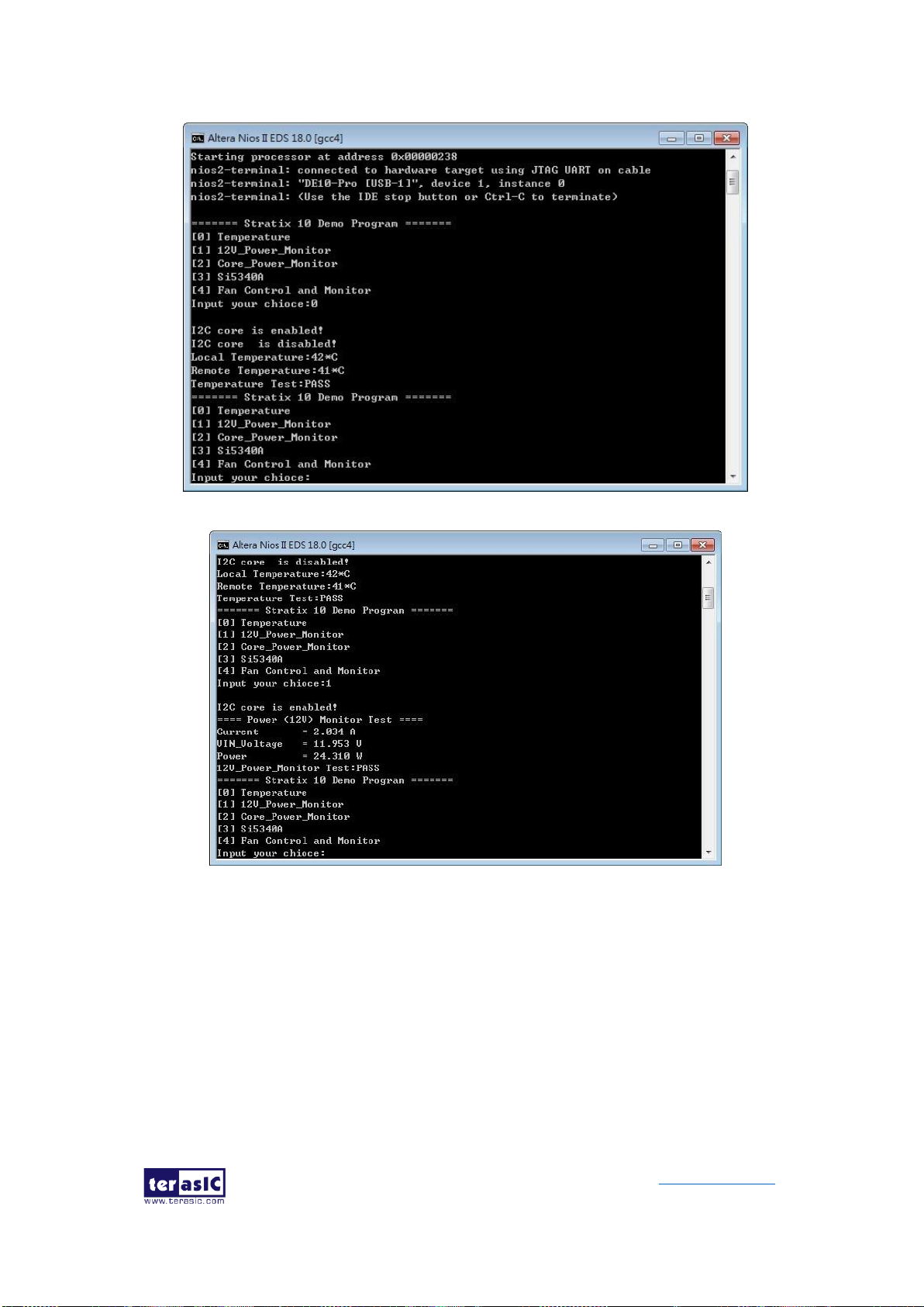
DE10-Pro
User Manual
98
www.terasic.com
September 24,
2019
Figure 5-10 Temperature Demo
Figure 5-11 12V power monitor Demo

DE10-Pro
User Manual
99
www.terasic.com
September 24,
2019
Figure 5-12 Core power monitor Demo
Figure 5-13 Si5340A Demo

DE10-Pro
User Manual
100
www.terasic.com
September 24,
2019
Figure 5-14 Fan Menu
Figure 5-15 Reading Fan Speed
 Loading...