


PCA3 User Manual
www.terasic.com
February 8, 2018
1
CONTENTS
Chapter 1 Introduction ..................................................................................................................... 2
1.1 Package Contents ........................................................................................................................................ 2
1.2 Features....................................................................................................................................................... 3
1.3 Getting Help ............................................................................................................................................... 4
Chapter 2 Architecture ..................................................................................................................... 5
2.1 Layout and Components ............................................................................................................................. 5
2.2 Block Diagram of the PCA3 card ............................................................................................................... 6
Chapter 3 Card Components ........................................................................................................... 8
3.1 PCIe Edge Connector ................................................................................................................................. 8
3.2 PCIe Cable Connector .............................................................................................................................. 10
3.3 LEDs ......................................................................................................................................................... 14
3.4 Lane Re-driver IC ..................................................................................................................................... 14
Chapter 4 Setup Example .............................................................................................................. 16
4.1 Introduction .............................................................................................................................................. 16
4.2 PC PCI Express Software SDK ................................................................................................................ 16
4.3 Reference Design - Fundamental ............................................................................................................. 28
4.4 PCIe Reference Design – DDR3 .............................................................................................................. 34
Chapter 5 Appendix ..................................................................................................................... 41
5.1 Revision History ....................................................................................................................................... 41
5.2 Copyright Statement ................................................................................................................................. 41
PCA3 User Manual
www.terasic.com
February 8, 2018
2
Chapter 1
Introduction
PCA3 (PCIe Cable Adapter, Gen 3) is a conversion card to connect boards with your host PC. It can
support up to PCIe Gen 3 x4. Users with boards such as Terasic TR4 and TR5 can establish
high-speed data transmission through this card and the PCIe cable via PCIe connector to any host
PC. It provides automatic rate-detect and adaptation to PCIe Gen-1, Gen-2, and Gen-3 speeds.
11..1
1
PPaacckkaaggee CCoonntteennttss
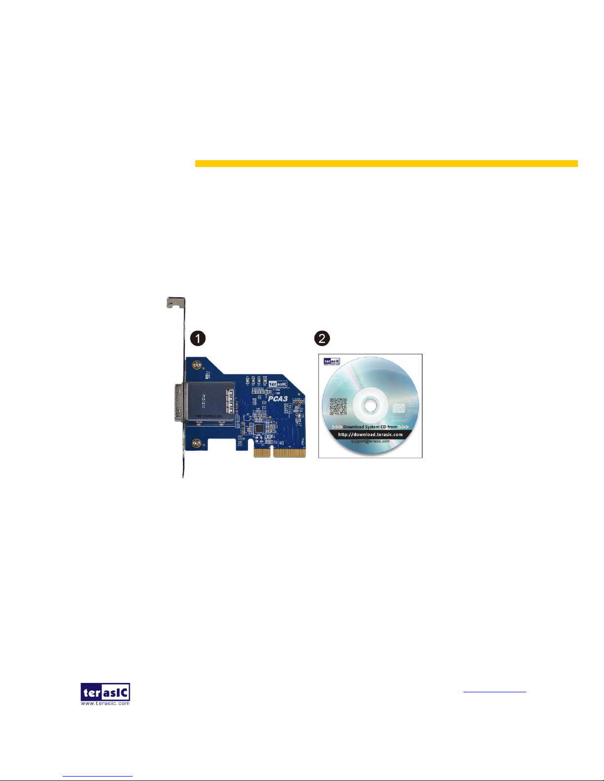
Figure 1-1 The PCA3 package contents
The PCA3 package includes:
PCA3 card
System CD Download Guide
PCA3 User Manual
www.terasic.com
February 8, 2018
3
11..2
2
FFeeaattuurreess
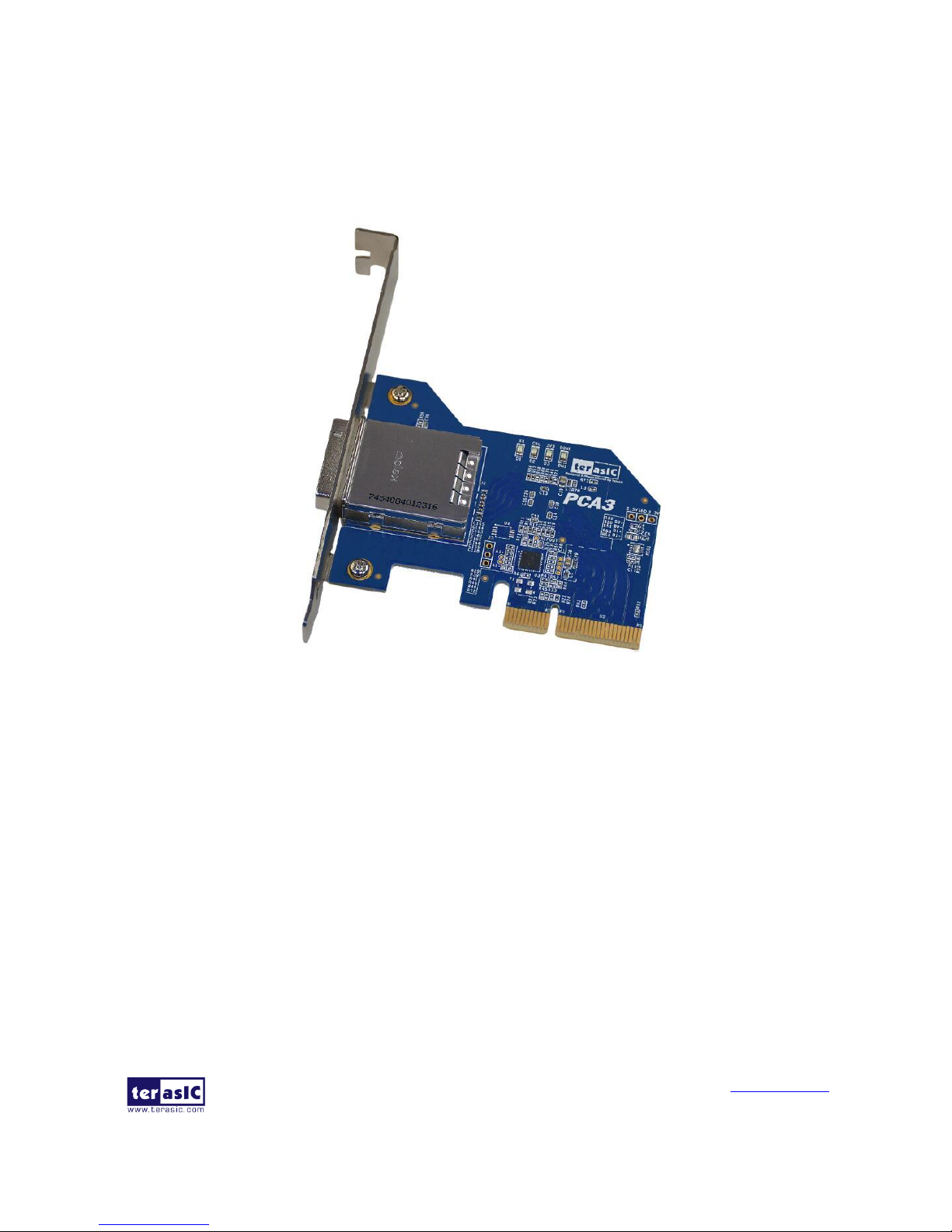
Figure 1- shows a photograph of the PCA3.
Figure 1-2 Exterior View
The key features of the card are listed below:
• Up to 8.0Gbps PCIe 3.0 Serial Re-Driver
• PCIe x4 Gen 3
• Adjustable receiver equalization
• Adjustable transmitter amplitude and de-emphasis

PCA3 User Manual
www.terasic.com
February 8, 2018
4
11..3
3
GGeettttiinngg HHeellpp
Here is information of how to get help if you encounter any problem:
Terasic Technologies
• Tel: +886-3-550-8800
• Email: support@terasic.com
PCA3 User Manual
www.terasic.com
February 8, 2018
5
Chapter 2
Architecture
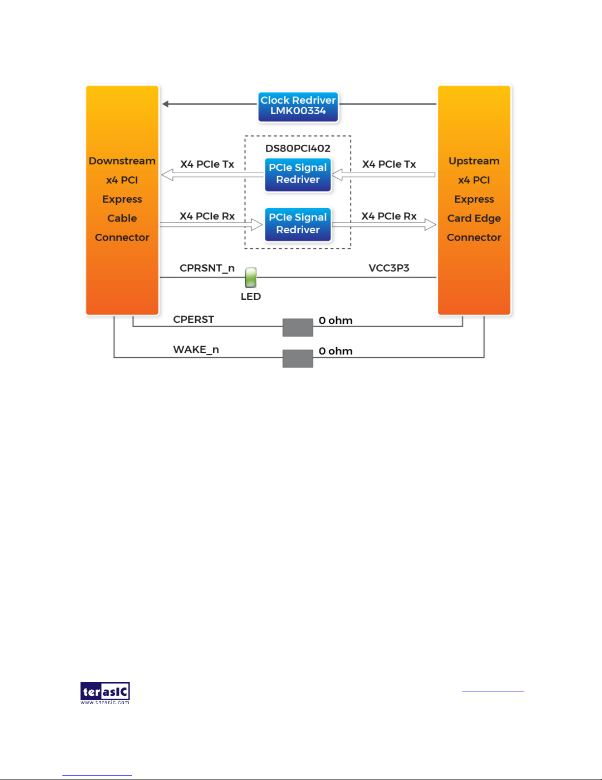
This chapter provides information about architecture and block diagram of the PCA3 card.
22..1
1
LLaayyoouutt aanndd CCoommppoonneennttss
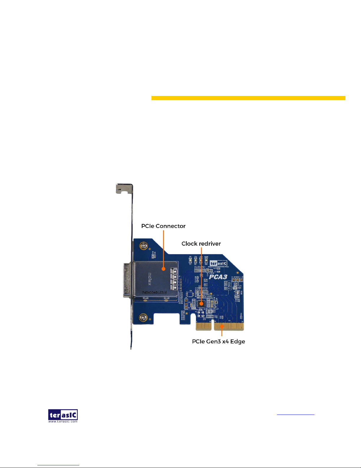
The picture of the Terasic PCIe x4 Cable Adapter (PCA3) is shown in Figure 2-1 and Figure 2-2. It
depicts the layout of the card and indicates the locations of the connectors and key components.
Figure 2-1 The PCA3 Card PCB and Component Diagram (top view)
PCA3 User Manual
www.terasic.com
February 8, 2018
6
Figure 2-2 The PCA3 Card PCB and Component Diagram (bottom view)
22..2
2
BBlloocckk DDiiaaggrraamm ooff tthhee PPCCAA33 ccaarrdd
Figure 2-3 shows the block diagram of the PCA3 card.
PCA3 User Manual
www.terasic.com
February 8, 2018
7
Figure 2-3 Block Diagram of PCA3
PCA3 User Manual
www.terasic.com
February 8, 2018
8
Chapter 3
Card Components
This chapter describes the specifications of the onboard components.
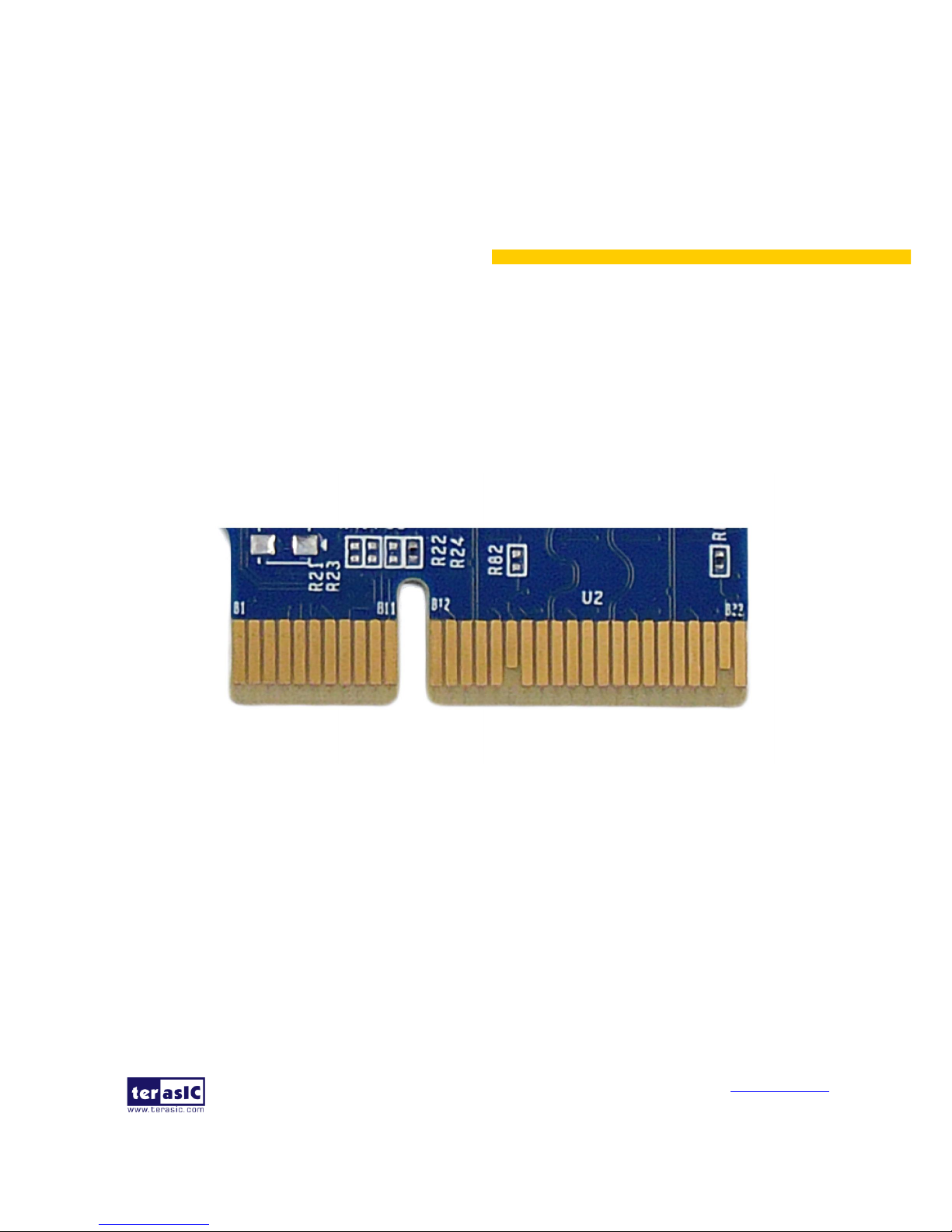
33..1
1
PPCCIIee EEddggee CCoonnnneeccttoorr
This PCIe edge connector is used to connect the PCA3 with PC motherboard PCIe slot, as show
Figure 3-1 and Figure 3-2.
Figure 3-1 PCA3 Edge Connector
PCA3 User Manual
www.terasic.com
February 8, 2018
9
Figure 3-2 Plug the PCA3 into the PCIe slot of the Motherboard
The pins are defined as shown in Table 3-1 with side A on the top of the center-line on the solder
side of the card and side B on the bottom of the centerline on the component side of the card.
The PCIe interface pins PETpx, PETnx, PERpx, and PERnx are named with the following
convention: “PE” stands for PCIe high speed, “T” for Transmitter, “R” for Receiver, “p” for
positive (+), and “n” for negative (-).
Note that adjacent differential pairs are separated by two ground pins to manage the connector
crosstalk.
Table 3-1 gives the wiring information of the PCIe Edge connector.
Table 3-1 Pin assignments and descriptions on PCIe Edge connector
Pin Numbers
Side B
Side A
Name
Description
Name
Description
1
NC
NC
PRSNT1n
Hot-Plug presence
detect
2
NC
NC
NC
NC 3 NC
NC
NC
NC 4 GND
Ground
GND
Ground
5
SMCLK
System Clock
NC
NC

PCA3 User Manual
www.terasic.com
February 8, 2018
10
6
SMDAT
System Data Line
NC
NC 7 GND
Ground
NC
NC 8 VCC3P3
3.3V Power
NC
NC 9 NC
NC
VCC3P3
3.3V Power
10
3.3VAUX
3.3 V Auxiliary
Power
VCC3P3
3.3V Power
11
WAKE
NC
PERSTn
Fundamental
Reset
Mechanical Key
12
RSVD
Reserved
GND
Ground
13
GND
Ground
REFCLK+
Reference clock
(differential
pair)
14
PETp0
Transmitter
differential pair,
Lane 0
REFCLK15
PETn0
GND
Ground
16
GND
Ground
PERp0
Receiver
differential pair,
Lane 0
17
PRSNT2n
Hot-Plug presence
detect
PERn0
18
GND
Ground
GND
Ground
19
PETp1
Transmitter
differential pair,
Lane 1
RSVD
Reserved
20
PETn1
GND
Ground
21
GND
Ground
PERp1
Receiver
differential pair,
Lane 1
22
GND
Ground
PERn1
23
PETp2
Transmitter
differential pair,
Lane 2
GND
Ground
24
PETn2
GND
Ground
25
GND
Ground
PERp2
Receiver
differential pair,
Lane 2
26
GND
Ground
PERn2
27
PETp3
Transmitter
differential pair,
Lane 3
GND
Ground
28
PETn3
GND
Ground
29
GND
Ground
PERp3
Receiver
differential pair,
Lane 3
30
RSVD
Reserved
PERn3
31
PRSNT2n
Hot-Plug presence
detect
GND
Ground
32
GND
Ground
RSVD
Reserved
33..2
2
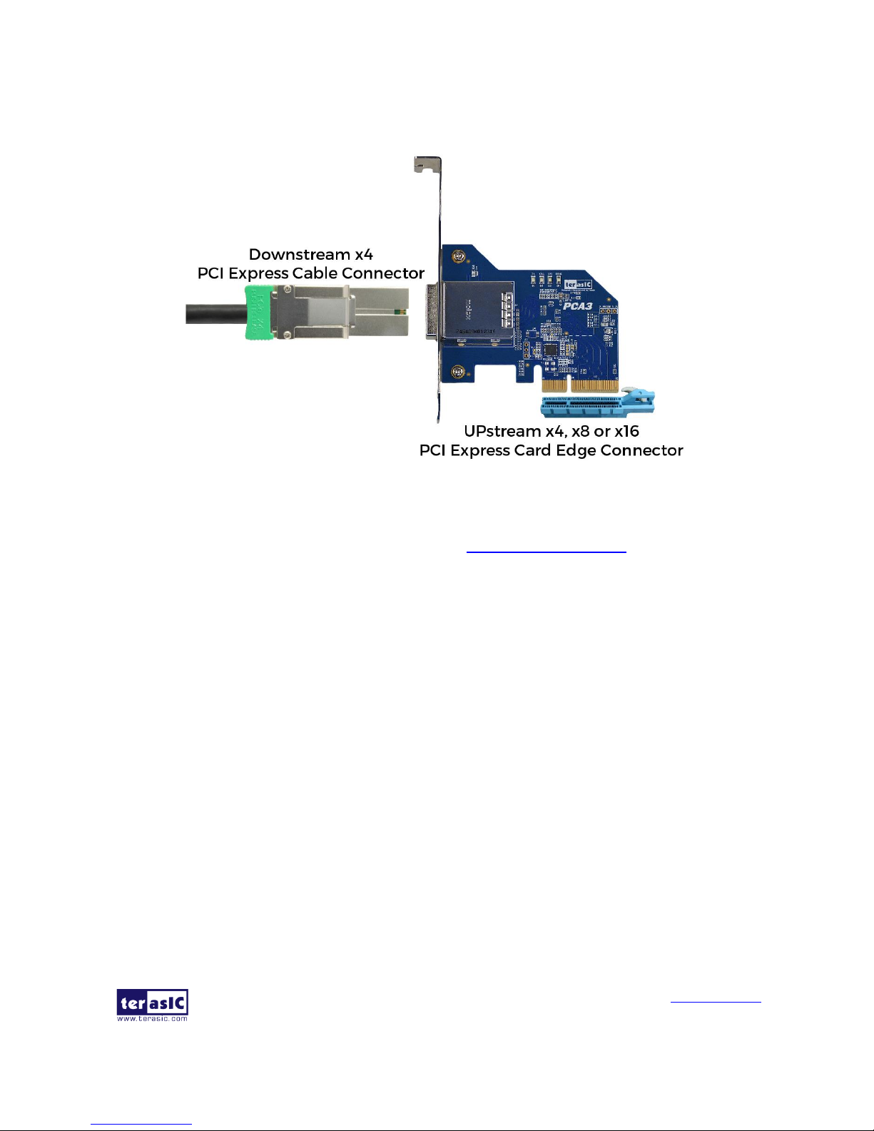
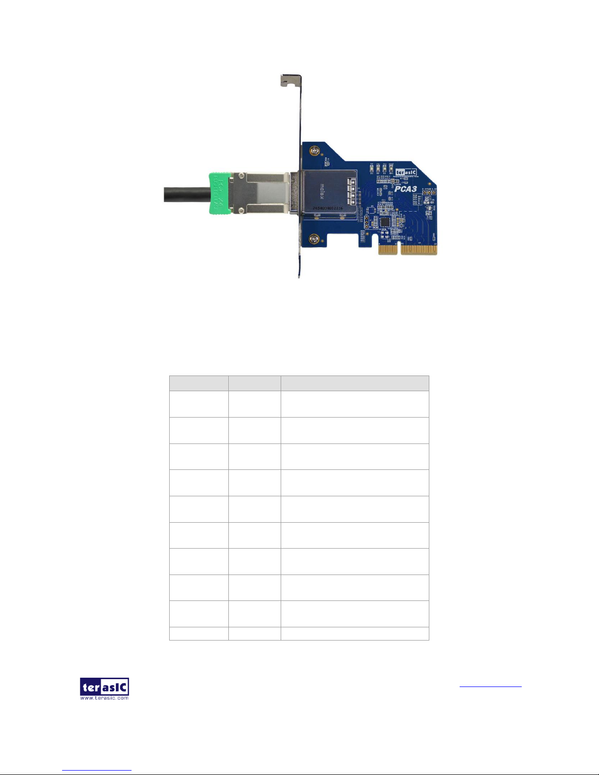
PPCCIIee CCaabbllee CCoonnnneeccttoorr
A PCIe cable connector is used to connect the PCIe x4 Cable and PCA cable connector, connect the
PCA3 User Manual
www.terasic.com
February 8, 2018
11
adapter by using a PCIe x4 Cable, as show Figure 3-3.
Figure 3-3 PCIe x4 Cable and PCA3
To purchase the PCIe x4 Cable, please refer to the url: PCIe_Cable.terasic.com.
Figure 3-4 shows the PCIe Cable connects PCA3 connector
PCA3 User Manual
www.terasic.com
February 8, 2018
12
Figure 3-4 PCIe Cable and PCA3 connector Connected
Table 3-2 gives the wiring information of the PCIe Cable connector.
Table 3-2 wiring information of the PCIe Cable connector
Pin Numbers
Name
Description
A1
GND
Ground reference for PCI
Express transmitter Lanes
A2
PETp0
Differential PCI Express
transmitter Lane 0
A3
PETn0
Differential PCI Express
transmitter Lane 0
A4
GND
Ground reference for PCI
Express transmitter Lanes
A5
PETp1
Differential PCI Express
transmitter Lane 1
A6
PETn1
Differential PCI Express
transmitter Lane 1
A7
GND
Ground reference for PCI
Express transmitter Lanes
A8
PETp2
Differential PCI Express
transmitter Lane 2
A9
PETn2
Differential PCI Express
transmitter Lane 2
A10
GND
Ground reference for PCI

PCA3 User Manual
www.terasic.com
February 8, 2018
13
Express transmitter Lanes
A11
PETp3
Differential PCI Express
transmitter Lane 3
A12
PETn3
Differential PCI Express
transmitter Lane 3
A13
GND
Ground reference for PCI
Express transmitter Lanes
A14
CREFCLK+
Differential 100MHz cable
reference clock
A15
CREFCLK-
Differential 100MHz cable
reference clock
A16
GND
Ground reference for PCI
Express transmitter Lanes
A17
SB_RTN
Signal return for single ended
sideband signals
A18
CPRSNTn
Used for detection of whether
a cable is installed and the
downstream subsystem is
powered
A19
CPWRON
Turns power on / off to slave type
downstream subsystems
B1
GND
Ground reference for PCI
Express transmitter Lanes
B2
PERp0
Differential PCI Express
receiver Lane 0
B3
PERn0
Differential PCI Express
receiver Lane 0
B4
GND
Ground reference for PCI
Express transmitter Lanes
B5
PERp1
Differential PCI Express
receiver Lane 1
B6
PERn1
Differential PCI Express
receiver Lane 1
B7
GND
Ground reference for PCI
Express transmitter Lanes
B8
PERp2
Differential PCI Express
receiver Lane 2
B9
PERn2
Differential PCI Express
receiver Lane 2
B10
GND
Ground reference for PCI
Express transmitter Lanes
B11
PERp3
Differential PCI Express
receiver Lane 3
B12
PERn3
Differential PCI Express

PCA3 User Manual
www.terasic.com
February 8, 2018
14
receiver Lane 3
B13
GND
Ground reference for PCI
Express transmitter Lanes
B14
PWR
+3.3VCable power
B15
PWR
+3.3VCable power
B16
PWR RTN
Cable power return
B17
PWR RTN
Cable power return
B18
CWAKEn
Power management signal for
wakeup events (optional)
B19
CPERSTn
Cable PERSTn
33..3
3
LLEEDDss
The PCA3 includes status LEDs, please refer to Table 3-3 for the status of the LED indicator.
Table 3-3 Status of the LED indicator
33..4
4
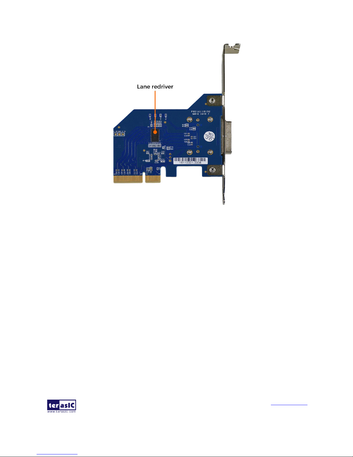
LLaannee RRee--ddrriivveerr IICC
A Lane Re-driver IC U1(DS80PCI402) is implemented on PCA3 card. In addition to supporting the
4-lane repeater function, DS80PCI402 chip also supports some modifiable parameters, such as
input equalization, internal Signal Detect Threshold and loopback function. These functions can be
set up by some of the resistances on PCA3 card, Figure 3-5 shows the resistances setting. Table 3-4
lists pin configuration and function.
Board
Reference
LED name
Description
D1
CBL
Cable PRSNT1n
D2
EDGE
Edge PRSNT1n
D3
POWER
Power LED

PCA3 User Manual
www.terasic.com
February 8, 2018
15
Figure 3-5 Resistances setting
Table 3-4 Pin configuration and function
Pin Numbers
Name
Description
19
EQA1
EQA1 control the level of equalization on the input pins. The pins are
active only when ENSMB is deasserted (low).
20
EQA0
EQA0 control the level of equalization on the input pins. The pins are
active only when ENSMB is deasserted (low).
21
RATE
RATE control pin selects GEN 1,2 and GEN 3 operating modes.
Tie 1kΩ to GND = GEN 1,2
FLOAT = AUTO Rate Select of Gen1/2 and Gen3 with de-emphasis
Tie 20kΩ to GND = GEN 3 without de-emphasis
Tied 1kΩ to VDD = RESERVED
22
RXDET
The RXDET pin controls the receiver detect function. Depending on the
input level, a 50Ω or > 50kΩ termination to the power rail is enabled.
23
LPBK
Controls the loopback function
Tie 1kΩ to GND = Root Complex Loopback (INA_n to OUTB_n)
Float = Normal Operation
Tie 1kΩ to VDD = End-point Loopback (INB_n to OUTA_n)
26
SD_TH/RD_EN
Controls the internal Signal Detect Threshold

PCA3 User Manual
www.terasic.com
February 8, 2018
16
Chapter 4
Setup Example
This chapter demonstrates how to use PCA3 daughtercard with FPGA host board. In the system CD,
we provide demonstration projects for Terasic TR4 and TR5 FPGA board. We will introduce how to
use PCA3 daughtercard and Terasic TR5 FPGA development board to communicate with the PC via
PCIe interface. For PCA3 with TR4 board, please refer to the CD
folder …/Demonstrations/TR4/doc/ for detailed document description.
44..1
1
IInnttrroodduuccttiioonn
The application reference design shows how to implement fundamental control and data transfer by
using PCIe port on the TR5. In the design, basic I/O is used to read or write the buttons and LEDs
on the TR5. High-speed data transfer is performed by DMA. Both Memory-Mapped and FIFO
memory types are demonstrated in the reference design. The demonstration also makes use of the
associated PCIe cable adapter card (PCA3). System Requirements
The following items are required for the PCA demonstration
• TR5 board x1
• PCA3 card x1
• PCIe x4 Cable x1
• PC x1
44..2
2
PPCC PPCCII EExxpprreessss SSooffttwwaarree SSDDKK
The CD contains a PC Windows based SDK to allow users to develop their 64-bits software
application on Windows XP/7/10 64-bits. The SDK is located in the “CDROM
\Demonstrations\TR5\PCIe_SW_KIT” folder which includes:
PCI Express Driver
PCI Express Library

PCA3 User Manual
www.terasic.com
February 8, 2018
17
PCI Express Examples
The kernel mode driver assumes the PCIe vender ID (VID) is 0x1172 and the device ID (DID) is
0xE003. If different VID and DID are used in the design, users need to modify the PCIe vender ID
(VID) and device ID (DID) in the driver INF file accordingly.
The PCI Express Library is implemented as a single DLL called TERASIC_PCIE_AVMM.DLL.
This file is a 64-bits DLL. With the DLL exported to the software API, users can easily
communicate with the FPGA. The library provides the following functions:
Basic Data Read and Write
Data Read and Write by DMA
For high performance data transmission, DMA is required as the read and write operations are
specified under the hardware design on the FPGA.
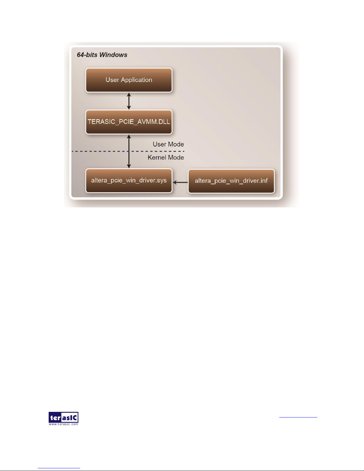
PCI Express Software Stack
Figure 7-8 shows the software stack for the PCI Express application software on 64-bit Windows.
The PCI Express driver incorporated in the DLL library is called TERASIC_PCIE_AVMM.dll.
Users can develop their applications based on this DLL. The altera_pcie_win_driver.sys kernel
driver is provided by Altera.
PCA3 User Manual
www.terasic.com
February 8, 2018
18
Figure 4-1 PCI Express Software Stack
Install PCI Express Driver on Windows
The PCIe driver is located in the folder:
“CDROM\Demonstrations\TR5\PCIe_SW_KIT\PCIe_Driver “
The folder includes the following four files:
Altera_pcie_win_driver.cat
Altera_pcie_win_driver.inf
Altera_pcie_win_driver.sys
WdfCoinstaller01011.dll
To install the PCI Express driver, execute the steps below:
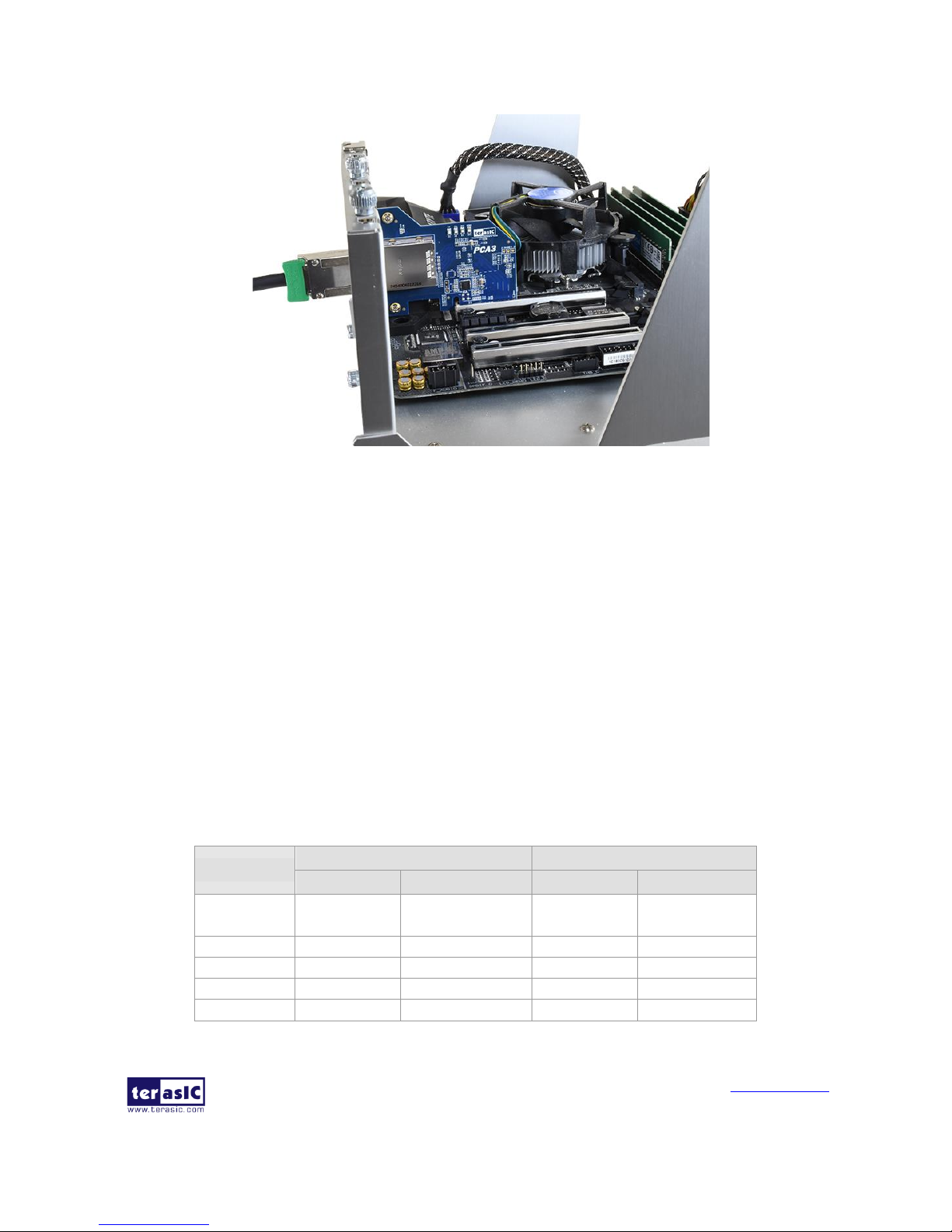
1. Make sure the TR5 and the PC are both powered off.
2. Plug the PCIe adapter card(PCA3) into the PCIe slot on the PC motherboard. Use the PCIe
cable to connect to the TR5 PCIE connector and the PCA3 (See Figure 4-2 )

PCA3 User Manual
www.terasic.com
February 8, 2018
19
Figure 4-2 FPGA board connect to PC
3. Power on your TR5 board and the host PC
4. Make sure Altera Programmer and USB-Blaster II driver are installed
5. Execute test.bat in “CDROM\Demonstrations\TR5\PCIe_Fundamental\demo_batch” to
configure the FPGA
6. Restart windows Operation System
7. Click the Control Panel menu from the Windows Start menu. Click the Hardware and the
Sound item before clicking the Device Manager to launch the Device Manager dialog. There
will be a PCI Device ite m in the dialog, as shown in Figure 4-3. Move the mouse cursor to
the PCI Device item and right click it to select the Update Driver Software... item.

PCA3 User Manual
www.terasic.com
February 8, 2018
20
Figure 4-3 Screenshot of launching Update Driver Software dialog
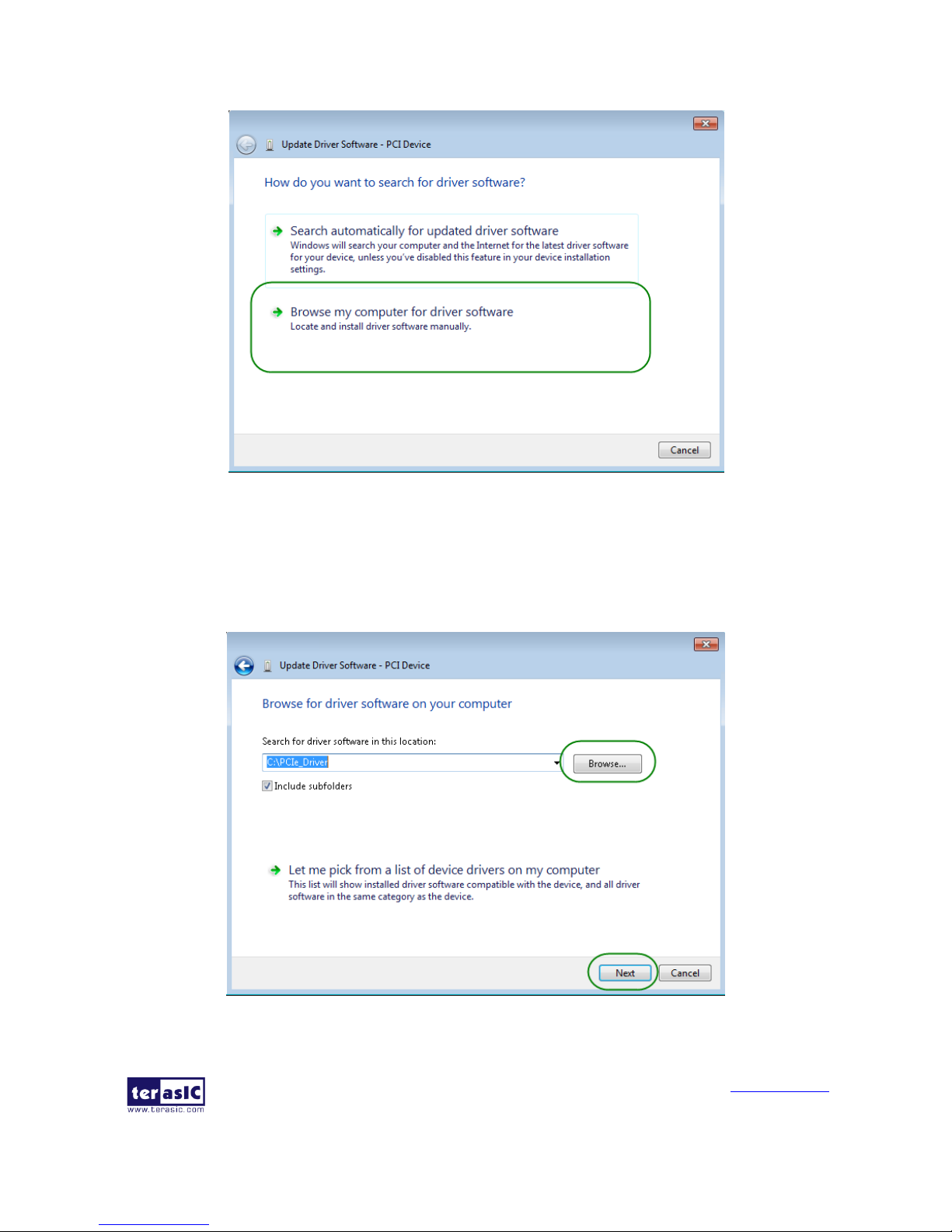
8. In the How do you want to search for driver software dialog, click Browse my computer
for driver software item, as shown in Figure 4-4. Click “OK” and then “Exit” to close the
installation program.
PCA3 User Manual
www.terasic.com
February 8, 2018
21
Figure 4-4 Dialog of Browse my computer for driver software
9. In the Browse for driver software on your computer dialog, click the Browse button to
specify the folder where altera_pcie_din_driver.inf is located, as shown in Figure 4-5 Click
the Next button.
Figure 4-5 Browse for driver software on your computer
PCA3 User Manual
www.terasic.com
February 8, 2018
22
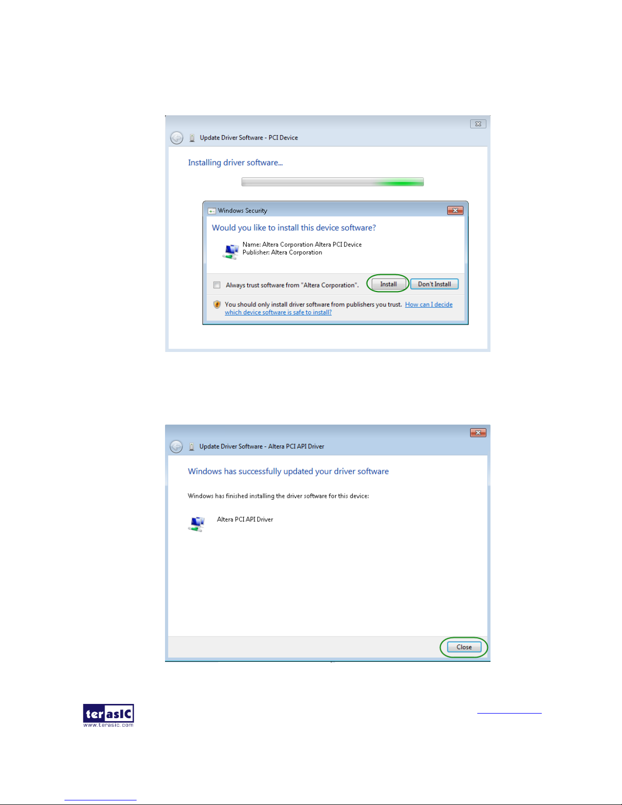
10. When the Windows Security dialog appears, as shown Figure 4-6 , click the Install button.
Figure 4-6 Click Install in the dialog of Windows Security
11. When the driver is installed successfully, the successfully dialog will appear, as shown in
Figure 4-7. Click the Close button.
PCA3 User Manual
www.terasic.com
February 8, 2018
23
Figure 4-7 Click Close when the installation of Altera PCI API Driver is complete
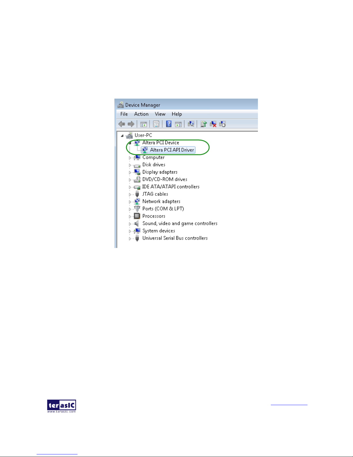
12. Once the driver is successfully installed, users can see the Altera PCI API Driver under the
device manager window, as shown in Figure 4-8.
Figure 4-8 Altera PCI API Driver in Device Manager
Create a Software Application
All necessary files to create a PCIe software application are located in the
CDROM\Demonstration\TR5\PCIe_SW_KIT\PCIe_Library, the files are as follows:
TERASIC_PCIE_AVMM.h
TERASIC_PCIE_AVMM.DLL (64-bit DLL)
Below lists the procedures to use the SDK files in users’ C/C++ project :
Create a 64-bit C/C++ project.
Include TERASIC_PCIE_AVMM.h in the C/C++ project.
PCA3 User Manual
www.terasic.com
February 8, 2018
24
Copy TERASIC_PCIE_AVMM.DLL to the folder where the project.exe is located.
Dynamically load TERASIC_PCIE_AVMM.DLL in C/C++ program. To load the DLL, please
refer to the PCIe fundamental example below.
Call the SDK API to implement the desired application.
TERASIC_PCIE.DLL/TERASIC_PCIEx64.DLL Software API
Users can easily communicate with the FPGA through the PCIe bus through the
TERASIC_PCIE_AVMM.DLL API. The details of API are described below:
PCIE_Open
Function:
Open a specified PCIe card with vendor ID, device ID, and matched card index.
Prototype:
PCIE_HANDLE PCIE_Open(
WORD wVendorID,
WORD wDeviceID,
WORD wCardIndex);
Parameters:
wVendorID:
Specify the desired vendor ID. A zero value means to ignore the vendor ID.
wDeviceID:
Specify the desired device ID. A zero value means to ignore the device ID.
wCardIndex:
Specify the matched card index, a zero based index, based on the matched vendor ID and
device ID.
Return Value:
Return a handle to presents specified PCIe card. A positive value is return if the PCIe card is
opened successfully. A value zero means failed to connect the target PCIe card.
This handle value is used as a parameter for other functions, e.g. PCIE_Read32.
Users need to call PCIE_Close to release handle once the handle is no more used.
PCIE_Close
Function:
Close a handle associated to the PCIe card.
Prototype:
void PCIE_Close(
PCIE_HANDLE hPCIE);
Parameters:
hPCIE:

PCA3 User Manual
www.terasic.com
February 8, 2018
25
A PCIe handle return by PCIE_Open function.
Return Value:
None.
PCIE_Read32
Function:
Read a 32-bit data from the FPGA board.
Prototype:
bool PCIE_Read32(
PCIE_HANDLE hPCIE,
PCIE_BAR PcieBar,
PCIE_ADDRESS PcieAddress,
DWORD * pdwData);
Parameters:
hPCIE:
A PCIe handle return by PCIE_Open function.
PcieBar:
Specify the target BAR.
PcieAddress:
Specify the target address in FPGA.
pdwData:
A buffer to retrieve the 32-bit data.
Return Value:
Return TRUE if read data is successful; otherwise FALSE is returned.
PCIE_Write32
Function:
Write a 32-bit data to the FPGA Board.
Prototype:
bool PCIE_Write32(
PCIE_HANDLE hPCIE,
PCIE_BAR PcieBar,
PCIE_ADDRESS PcieAddress,
DWORD dwData);
Parameters:

PCA3 User Manual
www.terasic.com
February 8, 2018
26
hPCIE:
A PCIe handle return by PCIE_Open function.
PcieBar:
Specify the target BAR.
PcieAddress:
Specify the target address in FPGA.
dwData:
Specify a 32-bit data which will be written to FPGA board.
Return Value:
Return TRUE if write data is successful; otherwise FALSE is returned.
PCIE_DmaRead
Function:
Read data from the memory-mapped memory of FPGA board in DMA.
Prototype:
bool PCIE_DmaRead(
PCIE_HANDLE hPCIE,
PCIE_LOCAL_ADDRESS LocalAddress,
void *pBuffer,
DWORD dwBufSize
);
Parameters:
hPCIE:
A PCIe handle return by PCIE_Open function.
LocalAddress:
Specify the target memory-mapped address in FPGA.
pBuffer:
A pointer to a memory buffer to retrieved the data from FPGA. The size of buffer should be
equal or larger the dwBufSize.
dwBufSize:
Specify the byte number of data retrieved from FPGA.
Return Value:
Return TRUE if read data is successful; otherwise FALSE is returned.
PCIE_DmaWrite
Function:
Write data to the memory-mapped memory of FPGA board in DMA.

PCA3 User Manual
www.terasic.com
February 8, 2018
27
Prototype:
bool PCIE_DmaWrite(
PCIE_HANDLE hPCIE,
PCIE_LOCAL_ADDRESS LocalAddress,
void *pData,
DWORD dwDataSize
);
Parameters:
hPCIE:
A PCIe handle return by PCIE_Open function.
LocalAddress:
Specify the target memory mapped address in FPGA.
pData:
A pointer to a memory buffer to store the data which will be written to FPGA.
dwDataSize:
Specify the byte number of data which will be written to FPGA.
Return Value:
Return TRUE if write data is successful; otherwise FALSE is returned.
PCIE_ConfigRead32
Function:
Read PCIe Configuration Table. Read a 32-bit data by given a byte offset.
Prototype:
bool PCIE_ConfigRead32 (
PCIE_HANDLE hPCIE,
DWORD Offset,
DWORD *pdwData
);
Parameters:
hPCIE:
A PCIe handle return by PCIE_Open function.
Offset:
Specify the target byte of offset in PCIe configuration table.
pdwData:
A 4-bytes buffer to retrieve the 32-bit data.
Return Value:
Return TRUE if read data is successful; otherwise FALSE is returned.

PCA3 User Manual
www.terasic.com
February 8, 2018
28
44..3
3
RReeffeerreennccee DDeessiiggnn -- FFuunnddaammeennttaall
The application reference design shows how to implement fundamental control and data transfer in
DMA. In the design, basic I/O is used to control the BUTTON and LED on the FPGA board.
High-speed data transfer is performed by DMA.
Demonstration Files Location
The demo file is located in the batch folder:
CDROM\demonstrations\TR5\PCIe_funcdamental\Demo_batch
The folder includes following files:
FPGA Configuration File: PCIe_funcdamental.sof
Download Batch file: test.bat
Windows Application Software folder : windows_app, includes
PCIE_FUNDAMENTAL.exe
TERASIC_PCIE_AVMM.dll
Demonstration Setup
1. Use the PCIe cable to connect to the TR5 PCIE connector and PCIe adapter card as
shown in Figure 4-9.
Figure 4-9 FPGA board connect to PC

PCA3 User Manual
www.terasic.com
February 8, 2018
29
2. Configure FPGA with PCIE_Fundamental.sof by executing the test.bat.
3. Install PCIe driver if necessary. The driver is located in the folder:
CDROM\Demonstration\TR5\PCIe_SW_KIT\PCIe_Driver.
4. Restart Windows
5. Make sure the Windows has detected the FPGA Board by checking the Windows
Control panel as shown in Figure 4-10.
Figure 4-10 Screenshot for PCIe Driver
6. Go to windows_app folder, execute PCIE_FUNDMENTAL.exe. A menu will appear
as shown in Figure 4-11.
Figure 4-11 Screenshot of Program Menu
7. Type 0 followed by a ENTER key to select Led Control item, then input 15 (hex 0x0f)
will make all led on as shown in Figure 4-12. If input 0(hex 0x00), all led will be

PCA3 User Manual
www.terasic.com
February 8, 2018
30
turned off.
Figure 4-12 Screenshot of LED Control
8. Type 1 followed by an ENTER key to select Button Status Read item. The button
status will be reported as shown in Figure 4-13.
Figure 4-13 Screenshot of Button Status Report
9. Type-2 followed by an ENTER key to select DMA Testing item. The DMA test result
will be reported as shown in Figure 4-14.

PCA3 User Manual
www.terasic.com
February 8, 2018
31
Figure 4-14 Screenshot of DMA Memory Test Result
10. Type 99 followed by an ENTER key to exit this test program
Development Tools
Quartus II 16.0
Visual C++ 2012
Demonstration Source Code Location
Quartus Project: Demonstrations\TR5\PCIE_Fundamental
Visual C++ Project: Demonstrations\TR5\PCIe_SW_KIT\PCIE_FUNDAMENTAL
PCA3 User Manual
www.terasic.com
February 8, 2018
32
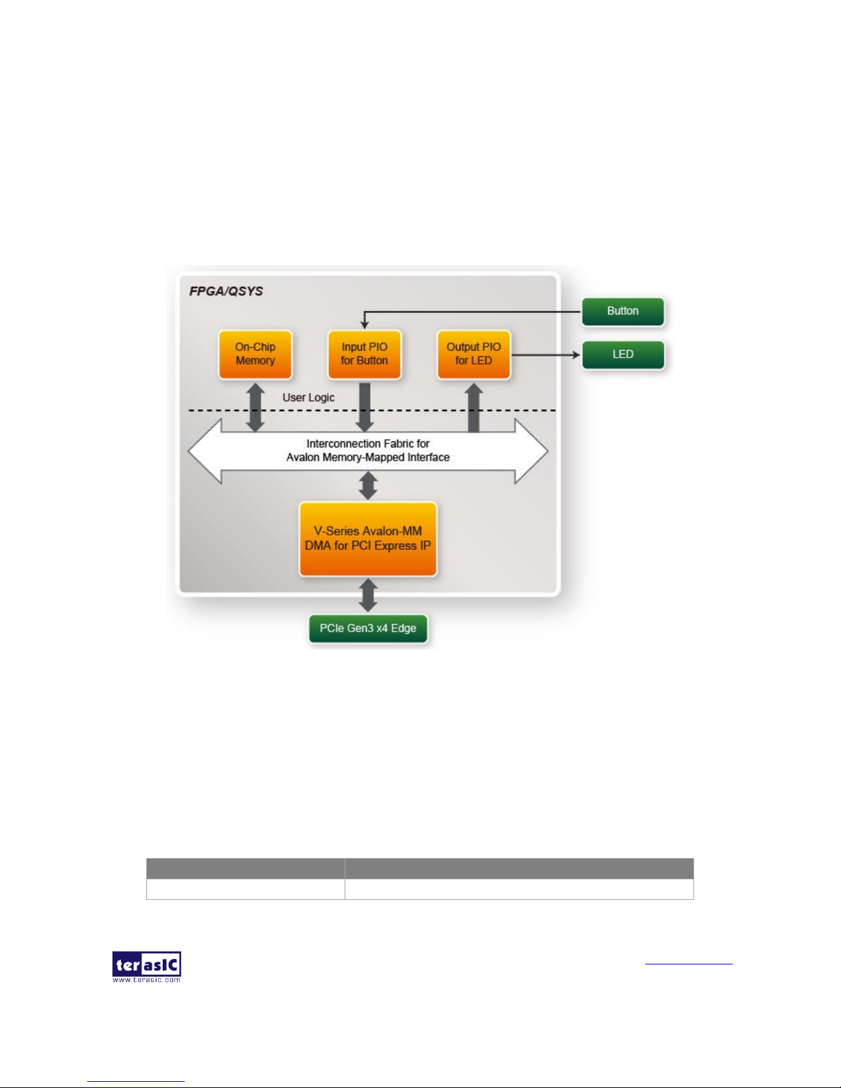
FPGA Application Design
Figure 4-15 shows the system block diagram in the FPGA system. In the Qsys, Altera PIO
controller is used to control the LED and monitor the Button Status, and the On-Chip memory is
used for performing DMA testing. The PIO controllers and the On-Chip memory are connected to
the PCI Express Hard IP controller through the Memory-Mapped Interface.
Figure 4-15 Hardware block diagram of the PCIe reference design
Windows Based Application Software Design
The application software project is built by Visual C++ 2012. The project includes the following
major files:
Name
Description
PCIE_FUNDAMENTAL.cpp
Main program

PCA3 User Manual
www.terasic.com
February 8, 2018
33
PCIE.c
Implement dynamically load for
TERAISC_PCIE_AVMM.DLL
PCIE.h
TERASIC_PCIE_AVMM.h
SDK library file, defines constant and data structure
The main program PCIE_FUNDAMENTAL.cpp includes the header file "PCIE.h" and defines the
controller address according to the FPGA design.
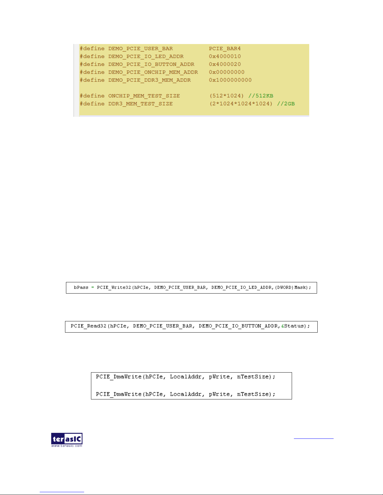
The base address of BUTTON and LED controllers are 0x4000010 and 0x4000020 based on
PCIE_BAR4, respectively. The on-chip memory base address is 0x00000000 relative to the DMA
controller.
Before accessing the FPGA through PCI Express, the application first calls PCIE_Load to
dynamically load the TERASIC_PCIE_AVMM.DLL. Then, it calls the PCIE_Open to open the PCI
Express driver. The constant DEFAULT_PCIE_VID and DEFAULT_PCIE_DID used in
PCIE_Open are defined in TERASIC_PCIE_AVMM.h. If developer changes the Vender ID,the
Device ID, and the PCI Express IP, they also need to change the ID value defined in
TERASIC_PCIE_AVMM.h. If the return value of the PCIE_Open is zero, it means the driver
cannot be accessed successfully. In this case, please make sure:
The FPGA is configured with the associated bit-stream file and the host is rebooted.
The PCI express driver is loaded successfully.
The LED control is implemented by calling PCIE_Write32 API, as shown below:
The button status query is implemented by calling the PCIE_Read32 API, as shown below:
The memory-mapped memory read and write test is implemented by PCIE_DmaWrite and
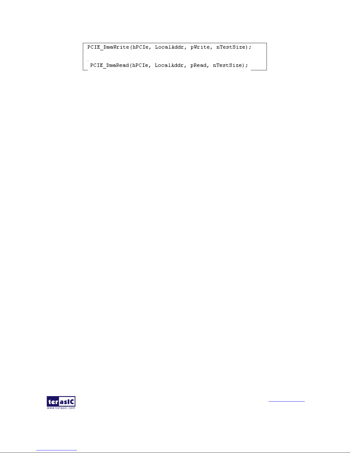
PCIE_DmaRead API, as shown below:
PCA3 User Manual
www.terasic.com
February 8, 2018
34
44..4
4
PPCCIIee RReeffeerreennccee DDeessiiggnn –– DDDDRR33
The application reference design shows how to add DDR3 Memory Controllers into the PCIe
Quartus project based on the PCI_Fundamental Quartus project and perform 2GB data DMA for
both SODIMM. Also, this demo shows how to call “PCIE_ConfigRead32” API to check PCIe link
status.
Demonstration Files Location
The demo file is located in the batch folder:
CDROM\Demonstrations\TR5\PCIe_DDR3\Demo_batch
The folder includes following files:
FPGA Configuration File: PCIe_DDR3.sof
Download Batch file: test.bat
Windows Application Software folder: windows_app, includes
PCIE_DDR3.exe
TERASIC_PCIE_AVMM.dll
Demonstration Setup
1. Install both DDR3 1600 2GB SODIMM on the FPGA board.
2. Use the PCIe cable to connect to the TR5 PCIE connector and PCIe adapter card.
3. Configure FPGA with PCIE_DDR3.sof by executing the test.bat.
4. Install PCIe driver if necessary.
5. Restart Windows
6. Make sure the Windows has detected the FPGA Board by checking the Windows
Control panel.
PCA3 User Manual
www.terasic.com
February 8, 2018
35
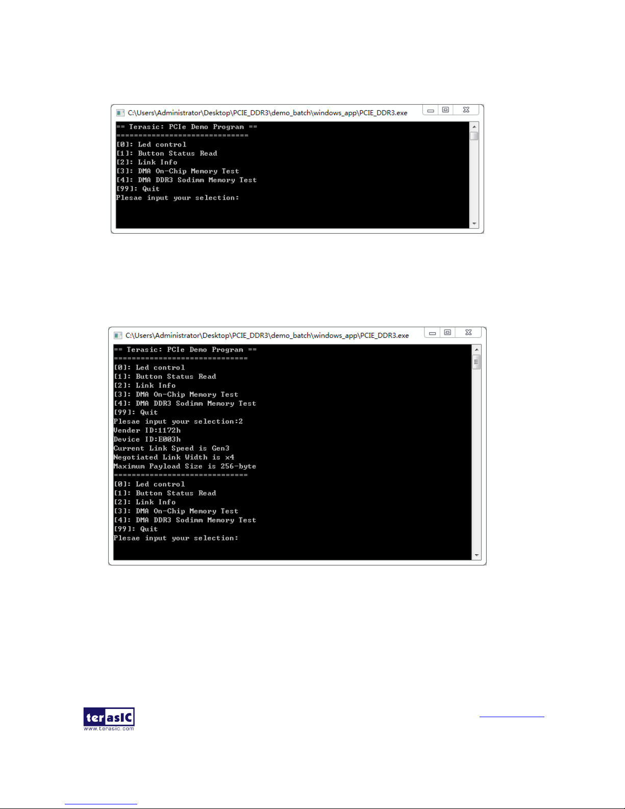
7. Goto windows_app folder, execute PCIE_DDR3.exe. A menu will appear as shown in
Figure 4-16.
Figure 4-16 Screenshot of Program Menu
8. Type 2 followed by the ENTER key to select Link Info item. The PICe link
information will be shown as in Figure 4-17. Gen3 link speed and x4 link width are
expected.
Figure 4-17 Screenshot of Link Info
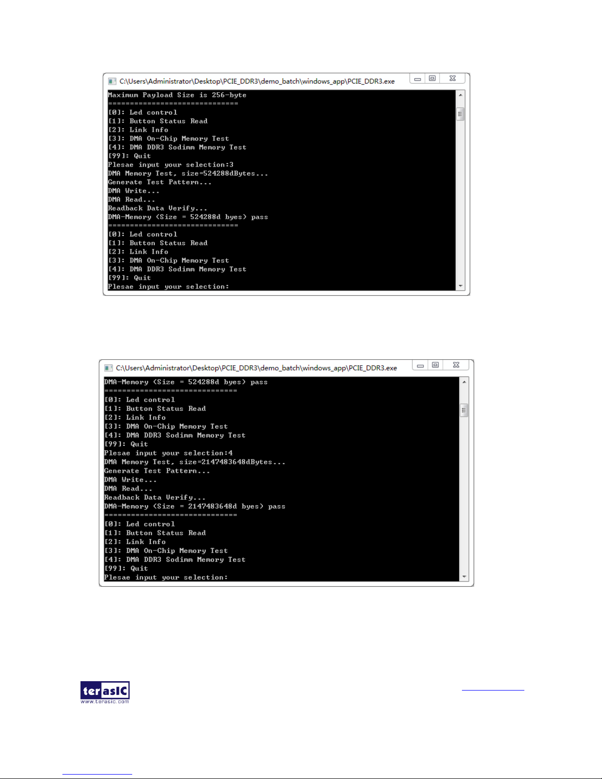
9. Type 3 followed by the ENTER key to select DMA On-Chip Memory Test item. The
DMA write and read test result will be reported as shown in Figure 4-18.
PCA3 User Manual
www.terasic.com
February 8, 2018
36
Figure 4-18 Screenshot of On-Chip Memory DMA Test Result
10. Type-4 followed by the ENTER key to select DMA DDR3 SODIMM Memory Test
item. The DMA write and read test result will be report as shown in Figure 4-19.
Figure 4-19 Screenshot of DDR3 SOSIMM Memory DAM Test Result
11. Type 99 followed by the ENTER key to exit this test program.

PCA3 User Manual
www.terasic.com
February 8, 2018
37
Development Tools
Quartus II 16.0
Visual C++ 2012
Demonstration Source Code Location
Quartus Project: Demonstrations\TR5\PCIE_DDR3
Visual C++ Project: Demonstrations\TR5\PCIe_SW_KIT\PCIe_DDR3
FPGA Application Design
Figure 4-20 shows the system block diagram in the FPGA system. In the Qsys, Altera PIO
controller is used to control the LED and monitor the Button Status, and the On-Chip memory and
DDR3 SODIMM Memory are used for performing DMA testing. The PIO controllers,the On-Chip
memory and DDR3 SODIMM Memory are connected to the PCI Express Hard IP controller
through the Memory-Mapped Interface.

PCA3 User Manual
www.terasic.com
February 8, 2018
38
Figure 4-20 Hardware block diagram of the PCIe DDR3 reference design
Windows Based Application Software Design
The application software project is built by Visual C++ 2012. The project includes the following
major files:
Name
Description
PCIE_DDR3.cpp
Main program
PCIE.c
Implement dynamically load for
TERAISC_PCIE_AVMM.DLL
PCIE.h
TERASIC_PCIE_AVMM.h
SDK library file, defines constant and data structure
The main program PCIE_DDR3.cpp includes the header file "PCIE.h" and defines the controller
address according to the FPGA design.
PCA3 User Manual
www.terasic.com
February 8, 2018
39
The base address of BUTTON and LED controllers are 0x4000010 and 0x4000020 based on
PCIE_BAR4, respectively. The on-chip memory base address is 0x00000000 relative to the DMA
controller. The above definition is the same as those in the PCIe Fundamental demo.
Before accessing the FPGA through PCI Express, the application first calls PCIE_Load to
dynamically load the TERASIC_PCIE_AVMM.DLL. Then, it calls PCIE_Open to open the PCI
Express driver. The constant DEFAULT_PCIE_VID and DEFAULT_PCIE_DID used in
PCIE_Open are defined in TERASIC_PCIE_AVMM.h. If the developer changes the Vender ID,
Device ID, and PCI Express IP, they also need to change the ID value defined in
TERASIC_PCIE_AVMM.h. If the return value of PCIE_Open is zero, it means the driver cannot
be accessed successfully. In this case, please make sure:
The FPGA is configured with the associated bit-stream file and the host is rebooted.
The PCI express driver is loaded successfully.
The LED control is implemented by calling PCIE_Write32 API, as shown below:
The button status query is implemented by calling the PCIE_Read32 API, as shown below:
The memory-mapped memory read and write test is implemented by PCIE_DmaWrite and
PCIE_DmaRead API, as shown below:

PCA3 User Manual
www.terasic.com
February 8, 2018
40
The pcie link information is implemented by PCIE_ConfigRead32 API, as shown below:

PCA3 User Manual
www.terasic.com
February 8, 2018
41
Chapter 5
Appendix
55..1
1
RReevviissiioonn HHiissttoorryy
Version
Change Log
V1.0
Initial Version (Preliminary)
V1.1
Add section 1.1 package contents and modify
55..2
2
CCooppyyrriigghhtt SSttaatteemmeenntt
Copyright © 2017 Terasic Technologies. All rights reserved.
 Loading...