

NET-FMC
User Manual
- 1 -
www.terasic.com
January 16, 2018

NET-FMC
User Manual
- 1 -
www.terasic.com
January 16, 2018
目錄
CHAPTER 1 ............................................... NET-FMC DEVELOPMENT KIT - 1 -
1-1 PACKAGE CONTENTS ......................................................................................... - 1 -
1-2 NET-FMC SYSTEM CD ..................................................................................... - 1 -
1-3 GETTING HELP ................................................................................................. - 1 -
CHAPTER 2 .............................. INTRODUCTION OF THE NET-FMC CARD - 2 -
2-1 FEATURES ....................................................................................................... - 3 -
2-2 BLOCK DIAGRAM OF THE NET-FMC BOARD.......................................................... - 3 -
2-3 CONNECTIVITY ................................................................................................. - 5 -
2-4 MODE SWITCH X 4 SETTING ............................................................................... - 5 -
CHAPTER 3 ............................................... USING THE NET-FMC BOARD - 8 -
3-1 ETHERNET PHY 88E1111 ................................................................................. - 8 -
3-2 FMC CONNECTOR ............................................................................................ - 9 -
CHAPTER 4 ................................................................. EXAMPLE CODES - 15 -
4-1 REMOTE UPDATE PORTAL ................................................................................. - 15 -
CHAPTER 5 ........................................................................... APPENDIX - 24 -
NET-FMC
User Manual
- 1 -
www.terasic.com
January 16, 2018
Chapter 1
NET-FMC Development Kit
1-1 Package Contents
The Terasic NET-FMC is a Gigabit Ethernet transceiver with an FMC interface. It offers
network transfers of up to 1 Gbps with the host board using an FMC connector. Also, it
provides a fully integrated Ethernet solution enabling fast implementation design,
shortening development times, and allows you to focus on the core functions of the system
design. Lastly, the NET-FMC can be connected any FMC(HPC) interfaces.
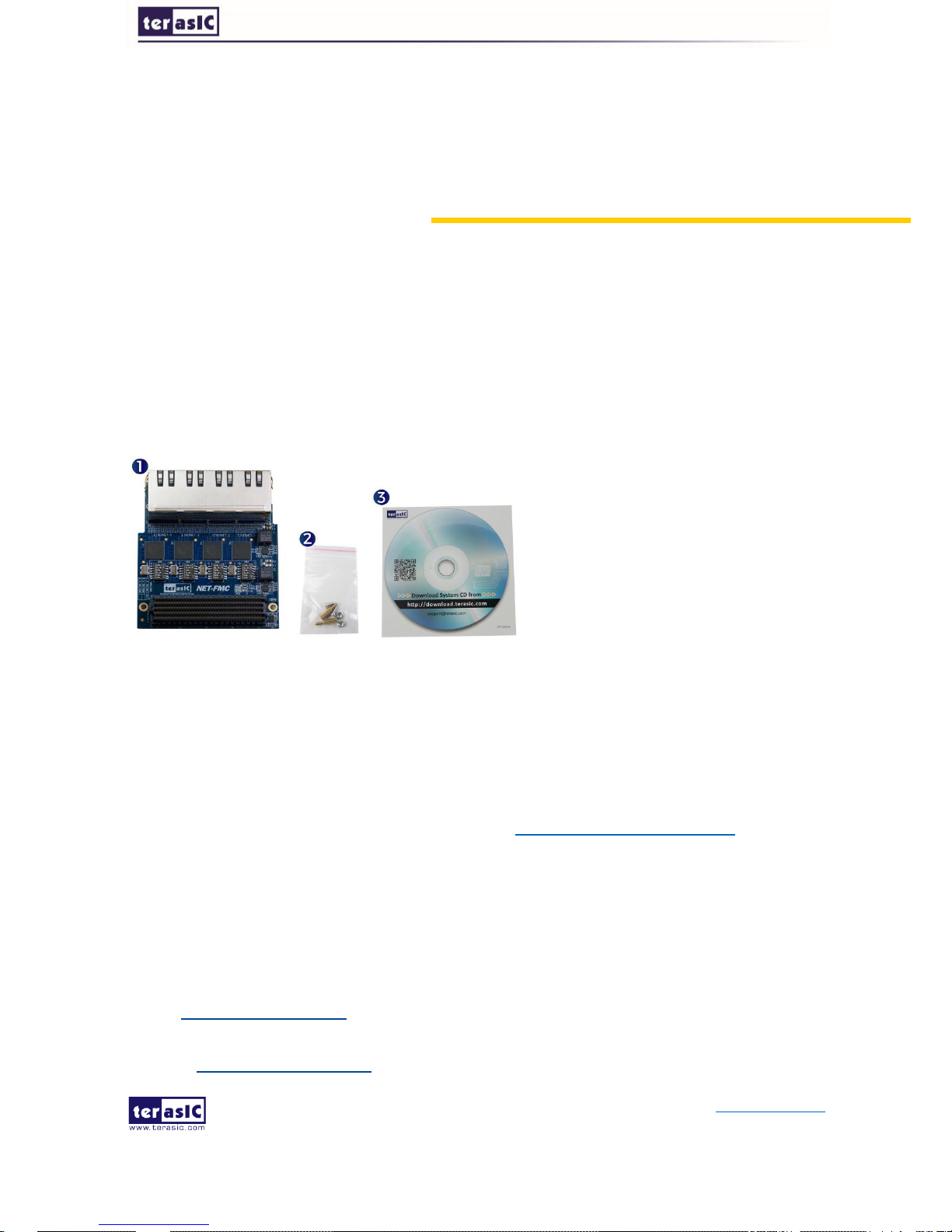
Figure 1-1 The NET-FMC package contents
1-2 NET-FMC System CD
The NET-FMC System CD contains all the documents and supporting materials associated
with NET-FMC, including the user manual, reference designs, and device datasheets.
Users can download this system CD from the link: http://net-fmc.terasic.com/cd
1-3 Getting Help
Here are the addresses where you can get help if you encounter any problems:
Terasic Technologies
9F., No.176, Sec.2, Gongdao 5th Rd, East Dist, Hsinchu City, 30070. Taiwan
Email: support@terasic.com
Tel.: +886-3-575-0880
Website: http://www.terasic.com
The NET-FMC package includes:
1. NET-FMC
2. Screw & Copper Pillar Pakage
3. CD Download Guide
NET-FMC
User Manual
- 2 -
www.terasic.com
January 16, 2018
Chapter 2
Introduction of the NET-FMC Card
This chapter describes the architecture and configuration of the NET-FMC Board including
block diagram and components related.
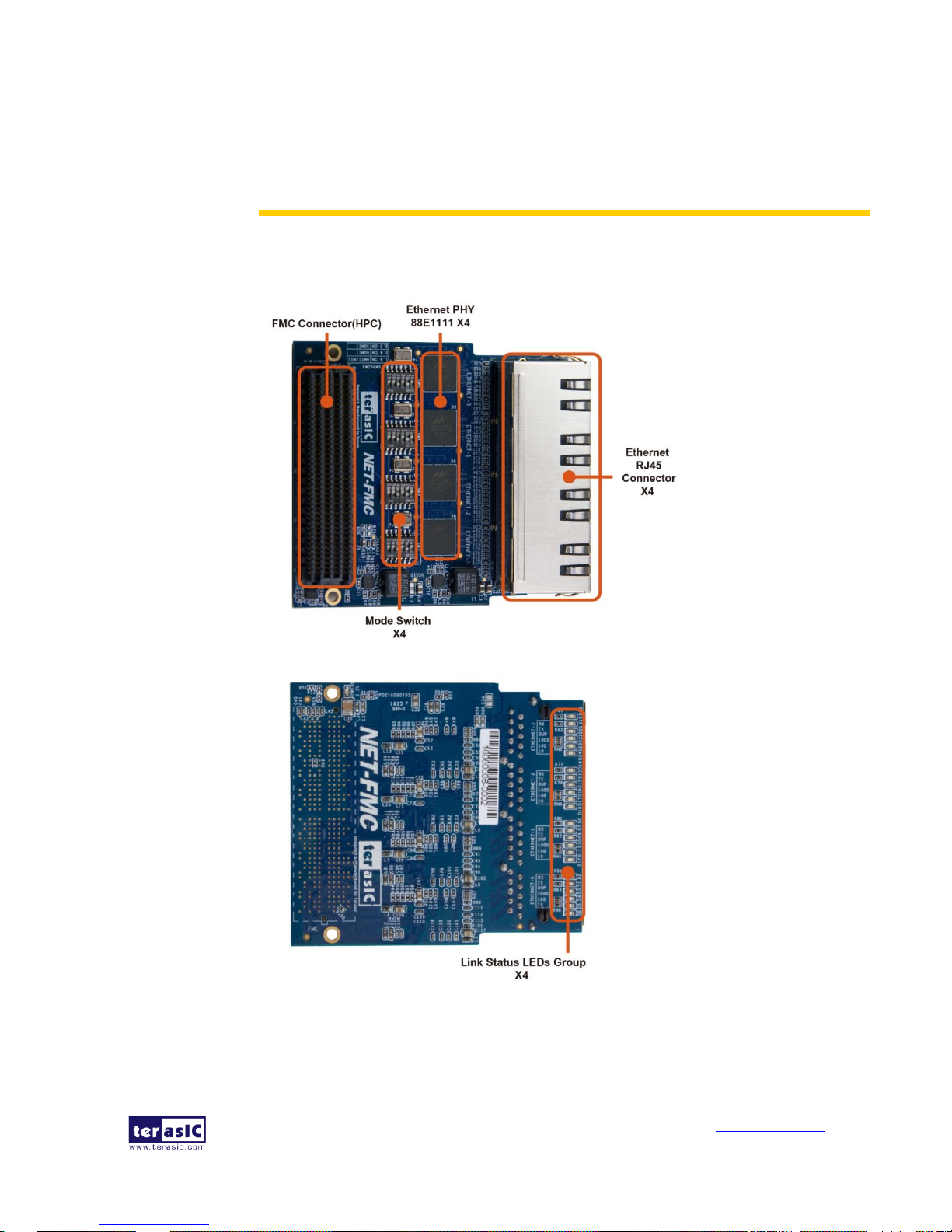
Figure 2-1 The NET-FMC Board PCB and Component Diagram of top side
Figure 2-2 The NET-FMC Board PCB and Component Diagram of bottom side
The photographs of the NET-FMC are shown in Figure 2-1 and Figure 2-2. They depict
the layout of the board and indicates the location of the connectors and the key
components on the top and bottom side.
The following components are provided on the NET-FMC Board:

NET-FMC
User Manual
- 3 -
www.terasic.com
January 16, 2018
Ethernet RJ45 Connector x4.
Ethernet PHY chip 88E1111 x4.
FMC Connector(HPC).
Mode Switch x4.
Link Status LEDs Group x4.
2-1 Features
The NET-FMC board has many features that allow users to implement a wide range of
design circuits, from simple circuits to various multimedia projects.
The following hardware is provided on the board:
Package Interface: VITA 57.1 FMC, 2.5V I/O-standard.
Ethernet PHY module:
Chip P/N: 88E1111.
10/100/1000BASE-T IEEE 802.3 compliant.
Support MAC Interface: GMII/MII, RGMII, SGMII.
Ethernet RJ45 Connector x4:
Use standard Cat 5 UTP cabling.
Mode Switch:
Support GMII/MII, RGMII, SGMII.
Four 25-MHz reference clock driven from dedicated oscillator.
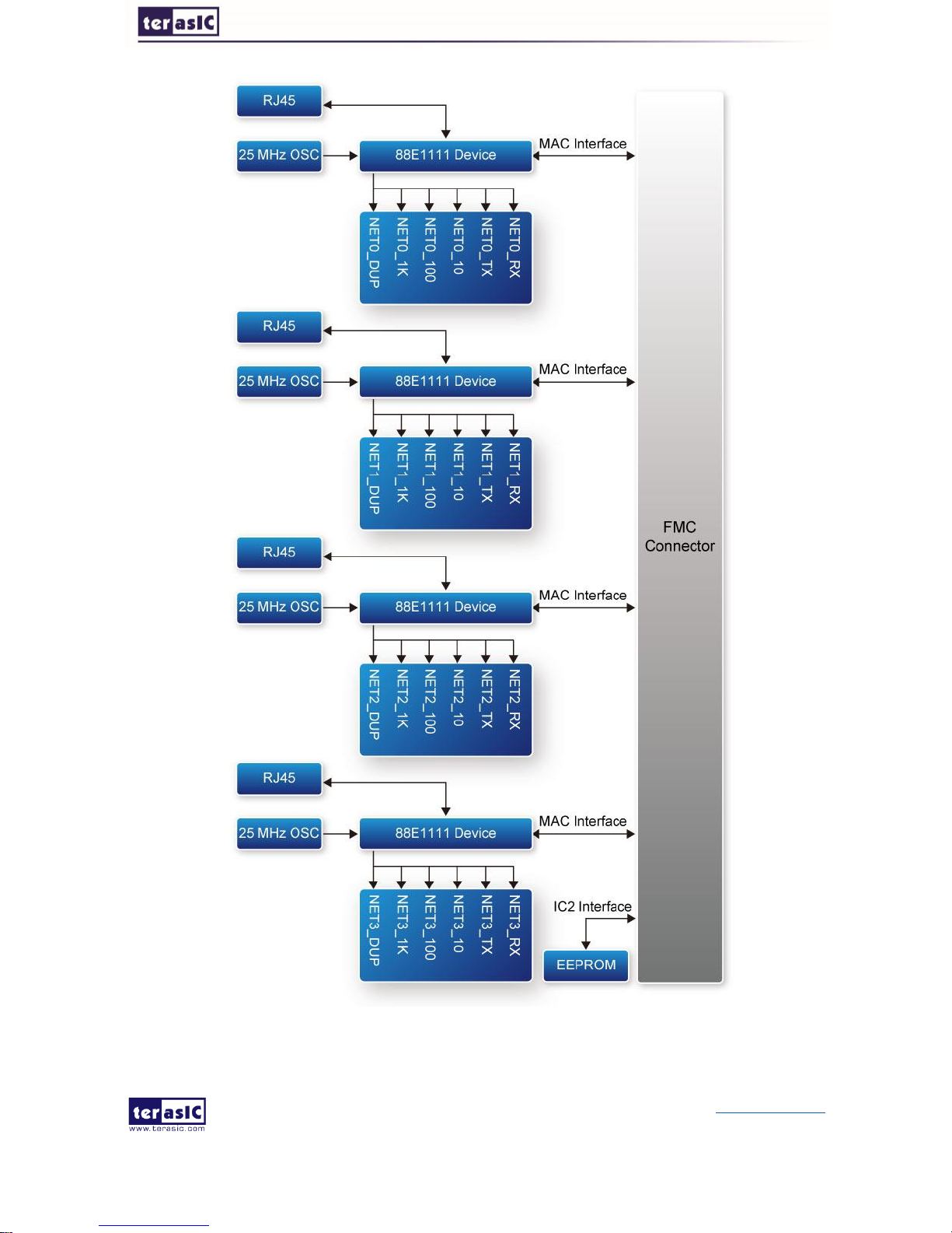
2-2 Block Diagram of the NET-FMC Board
Figure 2-3 shows the NET-FMC Block Diagram. Four 25 MHz reference clock driven from
dedicated oscillator are required for Ethernet PHY 88E1111. FMC Connector transmit the
data between host board and Ethernet PHY 88E1111 through MAC interface. Also,
four-port integrated 10/100/1000 Gigabit Ethernet Transceiver supported
SGMII/GMII/MII/RGMII MAC interfaces is installed for direct connection to a MAC/Switch
port. There are four group LEDs indicting the link status.
NET-FMC
User Manual
- 4 -
www.terasic.com
January 16, 2018
Figure 2-3 Block Diagram of NET-FMC Board
NET-FMC
User Manual
- 5 -
www.terasic.com
January 16, 2018
2-3 Connectivity
Terasic NET-FMC is able to connect to any FPGA development kit equipped with
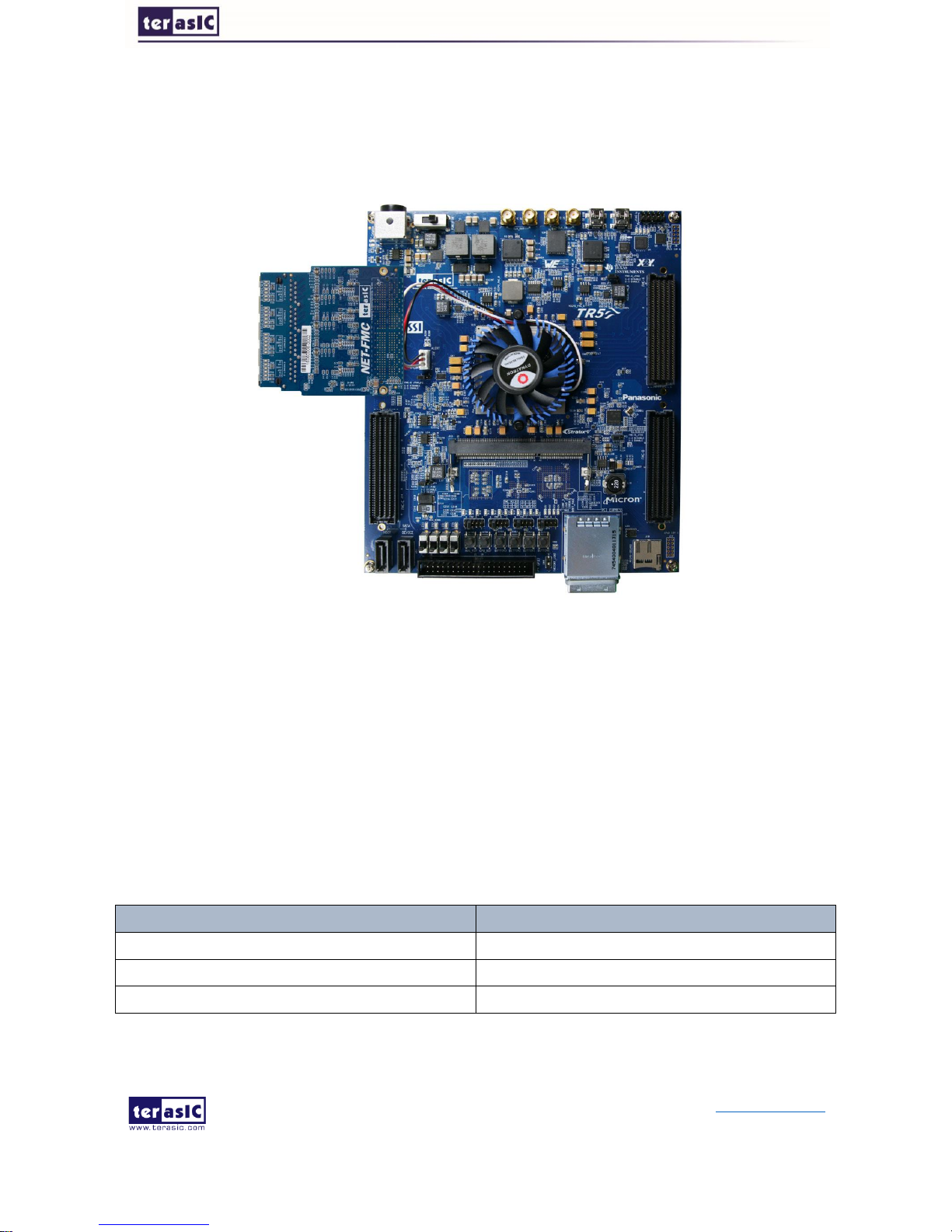
FMC(HPC) connector. The below picture Figure 2-4 shows the connections with TR5
board.
Figure 2-4 Connect the NET-FMC to TR5 board’s FMCD port
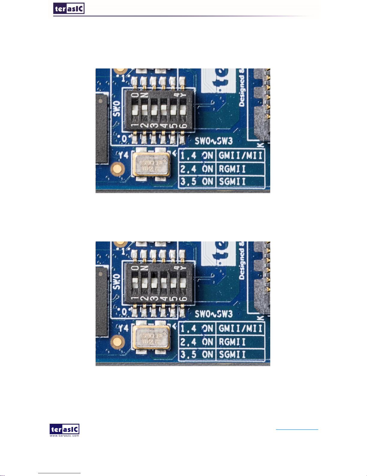
2-4 Mode Switch x 4 Setting
The NET_FMC card provides four Ethernet ports (ETH0 ~ETH3) via four Marvell 88E1111
Ethernet PHY chips. Each switch (SW0~SW3) is corresponding to one Ethernet port to
switch Ethernet port work modes from RGMII to GMII/MII or SGMII, SW0 is used for ETH0
port, SW1 is used for ETH1 port, SW2 is used for ETH2 port and SW3 is used for ETH3
port. Table 2-1 describes the working mode switch settings for ENET0 ~ ENET3 port work
modes.
Table 2-1 Mode Switch x 4 Setting for the Ethernet Mode
Mode Switch Setting
Ethernet Port Mode
1-ON,4-ON
GMII/MII
2-ON,4-ON
RGMII (default)
3-ON,5-ON
SGMII
NET-FMC
User Manual
- 6 -
www.terasic.com
January 16, 2018
The default setting of the Ethernet Port is SGMII mode. Users can change Ethernet mode
by using the Mode Switch x4. Take ETH0 as an example.
Set ETH0 MODE on the NET_FMC card to RGMII mode (default). The SW0[6:1] on
NET-FMC should be set to 001010, as shown in Figure 2-5.
Figure 2-5 SW0 setting for ETH0 port RGMII mode
Set ETH0 MODE on the NET_FMC card to GMII/MII mode. The SW0[6:1] on NET-FMC
should be set to 001001, as shown in Figure 2-6.
Figure 2-6 SW0 setting for ETH0 port GMII/MII mode

NET-FMC
User Manual
- 7 -
www.terasic.com
January 16, 2018
Set ETH0 MODE on the NET_FMC card to SGMII mode. The SW0[6:1] on NET-FMC
should be set to 010100, as shown in Figure 2-7.
Figure 2-7 SW0 setting for ETH0 port SGMII mode

NET-FMC
User Manual
- 8 -
www.terasic.com
January 16, 2018
Chapter 3
Using the NET-FMC Board
This chapter provides instructions on how to use Ethernet PHY 88E1111 and FMC
connector on the HDMI-FMC board.
3-1 Ethernet PHY 88E1111
Terasic NET-FMC Board equips with four Ethernet PHY named 88E1111, which is an
integrated 10/100/1000 ultra gigabit Ethernet transceiver device for Ethernet 10BASE-T,
100BASE-TX and 1000BASE-T applications. It contains all the active circuitry required to
implement the physical layer functions to transmit and receive data on standard CAT 5
unshielded twisted pair. The 88E1111 device supports the Gigabit Media Independent
Interface (GMII/MII), Reduced GMII (RGMII), and Serial Gigabit Media Independent
Interface (SGMII) for direct connection to a MAC/Switch port.
Figure 3-1 System Overview with 88E1111 device

NET-FMC
User Manual
- 9 -
www.terasic.com
January 16, 2018
Figure 3-1 shows the connections between the FMC (HPC), the 88E1111 Ethernet PHY,
and RJ-45 connector. Ethernet PHY 88E1111 function are controlled by the management
interface via NETx_MDC and NETx_MDIO. There is a LED used to indicate the status of
1000BASE-T link via NETx_LED_LINK1000.
The 88E1111 device incorporates the Marvell Virtual Cable Tester(VCT) feature, which
uses Time Domain Reflectometry(TDR) technology for the remote identification of potential
cable malfunctions, thus reducing equipment returns and service calls. Using VCT, the
88E1111 device detects and reports potential cabling issues such as pair swaps, pair
polarity and excessive pair skew.
The 88E1111 device uses advanced mixed-signal processing to perform equalization, echo
and crosstalk cancellation, data recovery, and error correction at a gigabit per second data
rate. The device achieves robust performance in noisy environments with very low power
dissipation.
3-2 FMC Connector
Table 3-1 shows the pin out and pin definitions of NET-FMC board.
Table 3-1 Pin Assignment of NET-FMC FMC interface
Signal Name
FMC Pin
Name/Number
Pin
Direction
Description
I/O
Standard
NET0_GTX_CLK
LA01_P_CC/D8
Output
Ethernet-0 GMII/TBI Transmit Clock
2.5V
NET0_TX_CLK
HA11_P/J12
Input
Ethernet-0 MII Transmit Clock, TBI 62.5
MHz Receive Clock 1
2.5V
NET0_TX_EN
LA08_P/G12
Output
Ethernet-0 GMII/MII Transmit Enable,
TBI Transmit Data 8
2.5V
NET0_TX_ER
HA14_P/J15
Output
Ethernet-0 GMII/MII Transmit Error, TBI
Transmit Data 9
2.5V
NET0_TX_D[0]
LA08_N/G13
Output
Ethernet-0 GMII/MII/TBI Transmit Data 0
2.5V
NET0_TX_D[1]
LA04_P/H10
Output
Ethernet-0 GMII/MII/TBI Transmit Data 1
2.5V
NET0_TX_D[2]
LA03_N/G10
Output
Ethernet-0 GMII/MII/TBI Transmit Data 2
2.5V
NET0_TX_D[3]
LA13_P/D17
Output
Ethernet-0 GMII/MII/TBI Transmit Data 3
2.5V
NET0_TX_D[4]
HA20_N/E19
Output
Ethernet-0 GMII/TBI Transmit Data 4
2.5V
NET0_TX_D[5]
HB03_N/E22
Output
Ethernet-0 GMII/TBI Transmit Data 5
2.5V
NET0_TX_D[6]
HB03_P/E21
Output
Ethernet-0 GMII/TBI Transmit Data 6
2.5V
NET0_TX_D[7]
HB05_P/E24
Output
Ethernet-0 GMII/TBI Transmit Data 7
2.5V
NET0_RX_CLK
LA13_N/D18
Input
Ethernet-0 GMII/MII Receive Clock, TBI
62.5 MHz Receive Clock 0
2.5V

NET-FMC
User Manual
- 10 -
www.terasic.com
January 16, 2018
NET0_RX_DV
LA05_N/D12
Input
Ethernet-0 GMII/MII Receive Valid, TBI
Transmit Data 8
2.5V
NET0_RX_ER
HA20_P/E18
Input
Ethernet-0 GMII/MII Receive Error, TBI
Transmit Data 9
2.5V
NET0_RX_D[0]
LA06_N/C11
Input
Ethernet-0 GMII/MII/TBI Receive Data 0
2.5V
NET0_RX_D[1]
LA05_P/D11
Input
Ethernet-0 GMII/MII/TBI Receive Data 1
2.5V
NET0_RX_D[2]
LA04_N/H11
Input
Ethernet-0 GMII/MII/TBI Receive Data 2
2.5V
NET0_RX_D[3]
LA06_P/C10
Input
Ethernet-0 GMII/MII/TBI Receive Data 3
2.5V
NET0_RX_D[4]
HA00_N_CC/F5
Input
Ethernet-0 GMII/TBI Receive Data 4
2.5V
NET0_RX_D[5]
HA07_P/J9
Input
Ethernet-0 GMII/TBI Receive Data 5
2.5V
NET0_RX_D[6]
HA03_P/J6
Input
Ethernet-0 GMII/TBI Receive Data 6
2.5V
NET0_RX_D[7]
HA00_P_CC/F4
Input
Ethernet-0 GMII/TBI Receive Data 7
2.5V
NET0_RX_CRS
CLK3_BIDIR_P/J
2
Input
Ethernet-0 GMII/MII Carrier Sense, TBI
Valid Comma Detect
2.5V
NET0_RX_COL
CLK3_BIDIR_N/J
3
Input
Ethernet-0 GMII/MII Collision, TBI Mode
Loopback
2.5V
NET0_S_CLKp
LA00_P_CC/G6
Input
Ethernet-0 SGMII 625 MHz Receive
Clock
2.5V
NET0_S_CLKn
LA00_N_CC/G7
Input
NET0_S_TX_p
HA04_P/F7
Output
Ethernet-0 SGMII Transmit Data
2.5V
NET0_S_TX_n
HA04_N/F8
Output
NET0_S_RX_p
HA05_P/E6
Input
Ethernet-0 SGMII Receive Data
2.5V
NET0_S_RX_n
HA05_N/E7
Input
NET0_MDC
LA03_P/G9
Output
Ethernet-0 Management Reference
Clock
2.5V
NET0_MDIO
LA02_N/H8
Inout
Ethernet-0 Management Data
2.5V
NET0_INT_n
CLK0_M2C_P
Input
Ethernet-0 Interrupt
2.5V
NET0_LED_LIN
K1000
HA02_P/K7
Input
Ethernet-0 Parallel LED output for
1000BASE-T link/speed or link indicator
2.5V
NET0_RST_n
LA02_P/H7
Output
Ethernet-0 Hardware Reset, active low
2.5V
NET1_GTX_CLK
LA01_N_CC/D9
Output
Ethernet-1 GMII/TBI Transmit Clock
2.5V
NET1_TX_CLK
HA19_N/F20
Input
Ethernet-1 MII Transmit Clock, TBI 62.5
MHz Receive Clock 1
2.5V
NET1_TX_EN
LA14_P/C18
Output
Ethernet-1 GMII/MII Transmit Enable,
TBI Transmit Data 8
2.5V
NET1_TX_ER
HB02_P/F22
Output
Ethernet-1 GMII/MII Transmit Error, TBI
Transmit Data 9
2.5V
NET1_TX_D[0]
LA14_N/C19
Output
Ethernet-1 GMII/MII/TBI Transmit Data 0
2.5V

NET-FMC
User Manual
- 11 -
www.terasic.com
January 16, 2018
NET1_TX_D[1]
LA17_P_CC/D20
Output
Ethernet-1 GMII/MII/TBI Transmit Data 1
2.5V
NET1_TX_D[2]
LA17_N_CC/D21
Output
Ethernet-1 GMII/MII/TBI Transmit Data 2
2.5V
NET1_TX_D[3]
LA18_P_CC/C22
Output
Ethernet-1 GMII/MII/TBI Transmit Data 3
2.5V
NET1_TX_D[4]
HB08_P/F28
Output
Ethernet-1 GMII/TBI Transmit Data 4
2.5V
NET1_TX_D[5]
HB07_P/J27
Output
Ethernet-1 GMII/TBI Transmit Data 5
2.5V
NET1_TX_D[6]
HB08_N/F29
Output
Ethernet-1 GMII/TBI Transmit Data 6
2.5V
NET1_TX_D[7]
HB11_P/J30
Output
Ethernet-1 GMII/TBI Transmit Data 7
2.5V
NET1_RX_CLK
LA12_N/G15
Input
Ethernet-1 GMII/MII Receive Clock, TBI
62.5 MHz Receive Clock 0
2.5V
NET1_RX_DV
LA11_N/H17
Input
Ethernet-1 GMII/MII Receive Valid, TBI
Transmit Data 8
2.5V
NET1_RX_ER
HA22_P/J21
Input
Ethernet-1 GMII/MII Receive Error, TBI
Transmit Data 9
2.5V
NET1_RX_D[0]
LA12_P/G15
Input
Ethernet-1 GMII/MII/TBI Receive Data 0
2.5V
NET1_RX_D[1]
LA11_P/H16
Input
Ethernet-1 GMII/MII/TBI Receive Data 1
2.5V
NET1_RX_D[2]
LA07_N/H14
Input
Ethernet-1 GMII/MII/TBI Receive Data 2
2.5V
NET1_RX_D[3]
LA07_P/H13
Input
Ethernet-1 GMII/MII/TBI Receive Data 3
2.5V
NET1_RX_D[4]
HB04_P/F25
Input
Ethernet-1 GMII/TBI Receive Data 4
2.5V
NET1_RX_D[5]
HB13_P/E30
Input
Ethernet-1 GMII/TBI Receive Data 5
2.5V
NET1_RX_D[6]
HB04_N/F26
Input
Ethernet-1 GMII/TBI Receive Data 6
2.5V
NET1_RX_D[7]
HB09_N/E28
Input
Ethernet-1 GMII/TBI Receive Data 7
2.5V
NET1_RX_CRS
HB05_N/E25
Input
Ethernet-1 GMII/MII Carrier Sense, TBI
Valid Comma Detect
2.5V
NET1_RX_COL
HB09_P/E27
Input
Ethernet-1 GMII/MII Collision, TBI Mode
Loopback
2.5V
NET1_S_CLKp
CLK1_M2C_P/G
2
Input
Ethernet-1 SGMII 625 MHz Receive
Clock
2.5V
NET1_S_CLKn
CLK1_M2C_N/G
3
Input
NET1_S_TX_p
HA08_P/F10
Output
Ethernet-1 SGMII Transmit Data
2.5V
NET1_S_TX_n
HA08_N/F11
Output
NET1_S_RX_p
HA09_P/E9
Input
Ethernet-1 SGMII Receive Data
2.5V
NET1_S_RX_n
HA09_N/E10
Input
NET1_MDC
LA10_N/C15
Output
Ethernet-1 Management Reference
Clock
2.5V
NET1_MDIO
LA09_N/D15
Inout
Ethernet-1 Management Data
2.5V
NET1_INT_n
LA10_P/C14
Input
Ethernet-1 Interrupt
2.5V

NET-FMC
User Manual
- 12 -
www.terasic.com
January 16, 2018
NET1_LED_LIN
K1000
HA02_N/K8
Input
Ethernet-1 Parallel LED output for
1000BASE-T link/speed or link indicator
2.5V
NET1_RST_n
LA09_P/D14
Output
Ethernet-1 Hardware Reset, active low
2.5V
NET2_GTX_CLK
LA16_P/G18
Output
Ethernet-2 GMII/TBI Transmit Clock
2.5V
NET2_TX_CLK
HA18_P/J18
Input
Ethernet-2 MII Transmit Clock, TBI 62.5
MHz Receive Clock 1
2.5V
NET2_TX_EN
LA15_N/H20
Output
Ethernet-2 GMII/MII Transmit Enable,
TBI Transmit Data 8
2.5V
NET2_TX_ER
HA19_P/F19
Output
Ethernet-2 GMII/MII Transmit Error, TBI
Transmit Data 9
2.5V
NET2_TX_D[0]
LA16_N/G19
Output
Ethernet-2 GMII/MII/TBI Transmit Data 0
2.5V
NET2_TX_D[1]
LA15_P/H19
Output
Ethernet-2 GMII/MII/TBI Transmit Data 1
2.5V
NET2_TX_D[2]
LA20_P/G21
Output
Ethernet-2 GMII/MII/TBI Transmit Data 2
2.5V
NET2_TX_D[3]
LA20_N/G22
Output
Ethernet-2 GMII/MII/TBI Transmit Data 3
2.5V
NET2_TX_D[4]
LA19_P/H22
Output
Ethernet-2 GMII/TBI Transmit Data 4
2.5V
NET2_TX_D[5]
LA19_N/H23
Output
Ethernet-2 GMII/TBI Transmit Data 5
2.5V
NET2_TX_D[6]
HB02_N/F23
Output
Ethernet-2 GMII/TBI Transmit Data 6
2.5V
NET2_TX_D[7]
HB01_P/J24
Output
Ethernet-2 GMII/TBI Transmit Data 7
2.5V
NET2_RX_CLK
LA30_P/H34
Input
Ethernet-2 GMII/MII Receive Clock, TBI
62.5 MHz Receive Clock 0
2.5V
NET2_RX_DV
LA31_P/G33
Input
Ethernet-2 GMII/MII Receive Valid, TBI
Transmit Data 8
2.5V
NET2_RX_ER
HB15_P/J33
Input
Ethernet-2 GMII/MII Receive Error, TBI
Transmit Data 9
2.5V
NET2_RX_D[0]
LA29_N/G31
Input
Ethernet-2 GMII/MII/TBI Receive Data 0
2.5V
NET2_RX_D[1]
LA28_N/H32
Input
Ethernet-2 GMII/MII/TBI Receive Data 1
2.5V
NET2_RX_D[2]
LA28_P/H31
Input
Ethernet-2 GMII/MII/TBI Receive Data 2
2.5V
NET2_RX_D[3]
LA29_P/G30
Input
Ethernet-2 GMII/MII/TBI Receive Data 3
2.5V
NET2_RX_D[4]
HB12_P/F31
Input
Ethernet-2 GMII/TBI Receive Data 4
2.5V
NET2_RX_D[5]
HB16_P/F34
Input
Ethernet-2 GMII/TBI Receive Data 5
2.5V
NET2_RX_D[6]
HB12_N/F32
Input
Ethernet-2 GMII/TBI Receive Data 6
2.5V
NET2_RX_D[7]
HB19_N/E34
Input
Ethernet-2 GMII/TBI Receive Data 7
2.5V
NET2_RX_CRS
HB13_N/E31
Input
Ethernet-2 GMII/MII Carrier Sense, TBI
Valid Comma Detect
2.5V
NET2_RX_COL
HB19_P/E33
Input
Ethernet-2 GMII/MII Collision, TBI Mode
Loopback
2.5V
NET2_S_CLKp
HA01_P_CC/E2
Input
Ethernet-2 SGMII 625 MHz Receive
2.5V

NET-FMC
User Manual
- 13 -
www.terasic.com
January 16, 2018
NET2_S_CLKn
HA01_N_CC/E3
Input
Clock
NET2_S_TX_p
HA12_P/F13
Output
Ethernet-2 SGMII Transmit Data
2.5V
NET2_S_TX_n
HA12_N/F14
Output
NET2_S_RX_p
HA13_P/E12
Input
Ethernet-2 SGMII Receive Data
2.5V
NET2_S_RX_n
HA13_N/E13
Input
NET2_MDC
LA21_N/H26
Output
Ethernet-2 Management Reference
Clock
2.5V
NET2_MDIO
LA22_N/G25
Inout
Ethernet-2 Management Data
2.5V
NET2_INT_n
LA21_P/H25
Output
Ethernet-2 Interrupt
2.5V
NET2_LED_LIN
K1000
HA06_P/K10
Input
Ethernet-2 Parallel LED output for
1000BASE-T link/speed or link indicator
2.5V
NET2_RST_n
LA22_P/G24
Input
Ethernet-2 Hardware Reset, active low
2.5V
NET3_GTX_CLK
LA30_N/H35
Output
Ethernet-3 GMII/TBI Transmit Clock
2.5V
NET3_TX_CLK
HB16_N/F35
Input
Ethernet-3 MII Transmit Clock, TBI 62.5
MHz Receive Clock 1
2.5V
NET3_TX_EN
LA33_P/G36
Output
Ethernet-3 GMII/MII Transmit Enable,
TBI Transmit Data 8
2.5V
NET3_TX_ER
HB18_P/J36
Output
Ethernet-3 GMII/MII Transmit Error, TBI
Transmit Data 9
2.5V
NET3_TX_D[0]
LA32_P/H37
Output
Ethernet-3 GMII/MII/TBI Transmit Data 0
2.5V
NET3_TX_D[1]
LA31_N/G34
Output
Ethernet-3 GMII/MII/TBI Transmit Data 1
2.5V
NET3_TX_D[2]
LA33_N/G37
Output
Ethernet-3 GMII/MII/TBI Transmit Data 2
2.5V
NET3_TX_D[3]
LA32_N/H38
Output
Ethernet-3 GMII/MII/TBI Transmit Data 3
2.5V
NET3_TX_D[4]
HA18_N/J19
Output
Ethernet-3 GMII/TBI Transmit Data 4
2.5V
NET3_TX_D[5]
HB01_N/J25
Output
Ethernet-3 GMII/TBI Transmit Data 5
2.5V
NET3_TX_D[6]
HA22_N/J22
Output
Ethernet-3 GMII/TBI Transmit Data 6
2.5V
NET3_TX_D[7]
HB11_N/J31
Output
Ethernet-3 GMII/TBI Transmit Data 7
2.5V
NET3_RX_CLK
LA18_N_CC/C23
Input
Ethernet-3 GMII/MII Receive Clock, TBI
62.5 MHz Receive Clock 0
2.5V
NET3_RX_DV
LA23_N/D24
Input
Ethernet-3 GMII/MII Receive Valid, TBI
Transmit Data 8
2.5V
NET3_RX_ER
LA23_P/D23
Input
Ethernet-3 GMII/MII Receive Error, TBI
Transmit Data 9
2.5V
NET3_RX_D[0]
LA27_N/C27
Input
Ethernet-3 GMII/MII/TBI Receive Data 0
2.5V
NET3_RX_D[1]
LA27_P/C26
Input
Ethernet-3 GMII/MII/TBI Receive Data 1
2.5V
NET3_RX_D[2]
LA26_P/D26
Input
Ethernet-3 GMII/MII/TBI Receive Data 2
2.5V
NET3_RX_D[3]
LA26_N/D27
Input
Ethernet-3 GMII/MII/TBI Receive Data 3
2.5V

NET-FMC
User Manual
- 14 -
www.terasic.com
January 16, 2018
NET3_RX_D[4]
HA07_N/J10
Input
Ethernet-3 GMII/TBI Receive Data 4
2.5V
NET3_RX_D[5]
HA14_N/J16
Input
Ethernet-3 GMII/TBI Receive Data 5
2.5V
NET3_RX_D[6]
HA11_N/J13
Input
Ethernet-3 GMII/TBI Receive Data 6
2.5V
NET3_RX_D[7]
HA03_N/J7
Input
Ethernet-3 GMII/TBI Receive Data 7
2.5V
NET3_RX_CRS
HB20_P/F37
Input
Ethernet-3 GMII/MII Carrier Sense, TBI
Valid Comma Detect
2.5V
NET3_RX_COL
HB20_N/F38
Input
Ethernet-3 GMII/MII Collision, TBI Mode
Loopback
2.5V
NET3_S_CLKp
HB21_P/E36
Input
Ethernet-3 SGMII 625 MHz Receive
Clock
2.5V
NET3_S_CLKn
HB21_N/E37
Input
NET3_S_TX_p
HA15_P/F16
Output
Ethernet-3 SGMII Transmit Data
2.5V
NET3_S_TX_n
HA15_N/F17
Output
NET3_S_RX_p
HA16_P/E15
Input
Ethernet-3 SGMII Receive Data
2.5V
NET3_S_RX_n
HA16_N/E16
Input
NET3_MDC
LA24_N/H29
Output
Ethernet-3 Management Reference
Clock
2.5V
NET3_MDIO
LA24_P/H28
Inout
Ethernet-3 Management Data
2.5V
NET3_INT_n
LA25_P/G27
Input
Ethernet-3 Interrupt
2.5V
NET3_LED_LIN
K1000
HA06_N/K11
Input
Ethernet-3 Parallel LED output for
1000BASE-T link/speed or link indicator
2.5V
NET3_RST_n
LA25_N/G28
Output
Ethernet-3 Hardware Reset, active low
2.5V

NET-FMC
User Manual
- 15 -
www.terasic.com
January 16, 2018
Chapter 4
Example Codes
This chapter provides Nios based examples for users to get started using the NET-FMC
board.
4-1 Remote Update Portal
A web server is implemented based on the socket’s application program interface (API)
provided by the NicheStack TCP/IP Stack Nios II Edition running on a MicroC/OS-II RTOS
to serve web content from the TR5 development board. Using DHCP protocol, the web
server is able to request a valid IP from the Gateway. The server can process basic
requests to serve HTML, JPEG, GIF, PNG, JS, CSS, SWF, ICO files from a single zip file
stored onto the flash memory on the TR5 board. User can remote update the web server by
rewrting the design files to the flash on the TR5 board.
Figure 4-1 shows the hardware setup of demonstration.
Figure 4-1 hardware setup of remote-update portal demonstration
Function block diagram
Figure 4-2 shows the function block diagram of remote-update portal demonstration.
Altera Triple Speed Ethernet is configured as 10/100/1000Mb Ethernet MAC with
1000BASE-X/SGMII PCS. A Generic Tri-state Controller(Flash Controller) is configured as
a 1Gb Flash controller to connect the off-chip Flash chip. The SGDMA-RX and SGDMA-TX

NET-FMC
User Manual
- 16 -
www.terasic.com
January 16, 2018
are used to transmit data between memory and Ethernet. The QSYS system requires one
50MHz clock resource and the Nios II program is reseting from Flash.
Figure 4-2 Function block diagram of remote-update portal demonstration
Design Tools
Quartus Prime 16.1
Nios II Eclipse 16.1
Demonstration Source Code
Quartus Prime project directory:
TR5_RevC_NET_FMCA_SGMII_update_portal_net0_161
Nios II Eclipse: TR5_RevC_NET_FMCA_SGMII_update_portal_net0_161\software
Nios Project Compilation
Before you attempt to compile the reference design under Nios II Eclipse, make sure the
project is cleaned first by clicking “Clean” from the “Project” menu of Nios II Eclipse.
Demonstration Batch File
Demo Batch File Folder:
TR5_RevC_NET_FMCA_SGMII_update_portal_net0_161\demo_batch
The demo batch file includes following files:

NET-FMC
User Manual
- 17 -
www.terasic.com
January 16, 2018
Batch file for USB-Blaster II: test.bat, test.sh
FPGA configure file: TR5_golden_top.sof
Nios II program: web_server.elf
Demonstration Setup
Please follow below procedures to setup the demonstrations.
Generate factory_web_server.pof file
Make sure Quartus Prime and Nios II are installed on your PC.
Execute the add_path.bat file in factory_pof directory to add your file location to
the .cof file. Or you will meet the error that hex files can not open.
Open the TR5_RevC_NET_FMCA_SGMII_update_portal_net0_161 project with
Quartus software.
Open the Convert Programming Files window.
Click the Open Conversion Setup Data button and choose the flash_web_server.cof
file in factory_pof directory as shown in Figure 4-3.
Figure 4-3 Selecting Conversion Setup Data
Add Sof and Hex Files. The files are added to the convert programmer defalt when

NET-FMC
User Manual
- 18 -
www.terasic.com
January 16, 2018
the .cof file openned as shown in Figure 4-4.
Figure 4-4 adding sof and hex files
Press Generate button to generate the new factory_web_server.pof in factory_pof
directory.
Write the factory_web_server.pof into Flash
Open Quartus Prime Programmer.
Connect a Mini USB Cable between the TR5 Board(J6) and the PC.
Open Hardware Setup window and choose DE5[USB-1] as shown in Figure 4-5.

NET-FMC
User Manual
- 19 -
www.terasic.com
January 16, 2018
Figure 4-5 Hardware Setup on TR5
Press add file and choose the TR5_PFL.sof in factory_pof directory.
Configure the FPGA by pressing Start button.
Press Auto Detect button after the FPGA configured successfully.
You will see a CFI_1Gb Flash detected on the JTAG chain. Press Yes to update the
device list as shown in Figure 4-6.
Figure 4-6 Updating the device
Use the mouse choose the CFI_1Gb device and press Change File button, browse to
the factory_pof directory and choose factory_web_server.pof file.
Check all the files Program and Verify option as in Figure 4-7 and press Start button
to write the Flash.

NET-FMC
User Manual
- 20 -
www.terasic.com
January 16, 2018
Figure 4-7 Program and Verify Options
Wait about 10 minutes until the pof file written to the flash successfully, then close the
software.
Get the IP address
Power down the TR5 board.
Set ETH0 MODE on the NET_FMC card to SGMII mode.The SW0[6:1] on NET-FMC
should be set to 010100.
Connect the RJ45 Ethernet cable to the ETHERNET-0 on NET_FMC daughter card.
Make sure the VDDJ for FMCA port on TR5 board is 2.5V. The 7&8 Pin of JP5 on TR5
board should be shorted.
Connect the NET_FMC card on FMCA (J11) port on TR5 mainboard. Please note the
demonstration is in FMCA, not in FMCD.
Set SW4(FACTORY_LOAD) on TR5 mainboard to 0.
Repower the board.
Open the nios2-terminal in Nios II Command Shell as shown in Figure 4-8. The
command shell is located in the Nios II EDS Installation dircetory, such as
D:\intelFPGA\16.1\nios2eds.

NET-FMC
User Manual
- 21 -
www.terasic.com
January 16, 2018
Figure 4-8 Open nios2 terminal in Nios II Command Shell
The first time you open the terminal, the system will request you to type four digital
number to generate the MAC address. You can type any 4 digital numbers as shown in
Figure 4-9.
Figure 4-9 type 4 digital numbers
Repower the Board again and use the nios2-terminal get the IP address as shown in
Figure 4-10. We use the ip address 192.168.21.102 for example.

NET-FMC
User Manual
- 22 -
www.terasic.com
January 16, 2018
Figure 4-10 get the ip address
Type the IP address in your web browser as shown in Figure 4-11, then you can
access the web content.
Figure 4-11 access the web content in browser

NET-FMC
User Manual
- 23 -
www.terasic.com
January 16, 2018
Remote update your design
Create your custom Quartus project. If your project contains a nios II system with a
software, you should add a CFI_Flash device on address map 0x00000000 and set
the nios2 reset vector to the Flash device. The offset should be 0x071c0000.
In Nios II Command Shell, convert your custom sof and elf file to flash file with the
below commands.
For sof files:
sof2flash --input=xxxx.sof --output=xxx.flash --offset=0x02940000 --pfl --optionbit=0x00030000
--programmingmode=FPP (the sof file name should be changed according to your quartus project name)
For elf file:
elf2flash --base=0x00000000 --end=0x07FFFFFF --reset=0x071c0000 --input=xxx.elf --output=xxx.flash
--boot=$SOPC_KIT_NIOS2/components/altera_nios2/boot_loader_cfi.srec (the elf file name should be changed
according to your nios2 software project name)
you can use the batch file in flash_convert directory to convert your sof and elf to flash
In the web page, choose your hardware and software flash files, then press the Upload
button to starting write your design files to the Flash on TR5 board.
The browser will goto the reset_system page when the write process finished.
Set the FACTORY_LOAD switch (SW4) to 1 and the BOOT_PAGE LED(D24) light on.
Press the MAX_RST(BUTTON5), the FPGA will be configured with your design.

NET-FMC
User Manual
- 24 -
www.terasic.com
January 16, 2018
Chapter 5
Appendix
Revision History
Version
Change Log
V1.0
Initial Version
V1.1
Add Section 2.4 Mode Switch x 4 Setting
Copyright Statement
Copyright © 2017 Terasic Inc. All rights reserved.
 Loading...