

Page 1
p
Page 2

MLT2 User Manual
1
www.terasic.com
April 12, 2016
CONTENTS
Chapter 1 Introduction ..................................................................................................................... 3
1.1 About the Package ...................................................................................................................................... 3
1.2 External Power Supply for MTL2 .............................................................................................................. 4
1.3 Assembly .................................................................................................................................................... 5
1.4 Connectivity ............................................................................................................................................... 6
1.5 Getting Help ............................................................................................................................................... 7
Chapter 2 Architecture of MTL2 ....................................................................................................... 8
2.1 Features....................................................................................................................................................... 8
2.2 MTL2 Kit.................................................................................................................................................... 8
2.3 Component and Layout .............................................................................................................................. 8
2.4 IDE Cable ................................................................................................................................................. 11
2.5 ITG Adapter .............................................................................................................................................. 11
Chapter 3 Using the MTL2 ............................................................................................................. 13
3.1 Pin Definition of 2x20 GPIO Connector .................................................................................................. 13
3.2 Using LCD................................................................................................................................................ 15
3.3 Using Terasic Multi-touch IP .................................................................................................................... 16
Chapter 4 ePhoto Demonstration ................................................................................................... 20
4.1 Operation Description .............................................................................................................................. 20
4.2 Block Diagram of the ePhoto Design ....................................................................................................... 21
4.3 Loading Photos into FLASH .................................................................................................................... 22
4.4 Demonstration for Terasic DE2-115 FPGA Board ................................................................................... 23
4.5 Custom Display Photo .............................................................................................................................. 24
Chapter 5 Painter Demonstration ................................................................................................... 26
5.1 Operation Description .............................................................................................................................. 26
5.2 System Description ................................................................................................................................... 27
Page 3

MLT2 User Manual
2
www.terasic.com
April 12, 2016
5.3 Demonstration for Terasic DE2-115 FPGA Board ................................................................................... 28
5.4 Demonstration Source Code ..................................................................................................................... 30
Chapter 6 Appendix ....................................................................................................................... 31
6.1 Revision History ....................................................................................................................................... 31
6.2 Copyright Statement ................................................................................................................................. 31
Page 4

MLT2 User Manual
3
www.terasic.com
April 12, 2016
Chapter 1
Introduction
The New Terasic Multi-touch LCD Module Second Edition (MTL2) is an all-purpose capacitive
touch-screen for FPGA applications and provides five points multi-touch gesture support. An IDE
cable with an IDE to GPIO (ITG) adapter is used to interface with various Terasic FPGA
development boards through a 2x20 GPIO interface on the MTL2. The kit contains complete
reference designs and source code for an ePhoto demonstration and Painter application. This
chapter provides the key information about the kit.
11..1
1
AAbboouutt tthhee PPaacckkaaggee
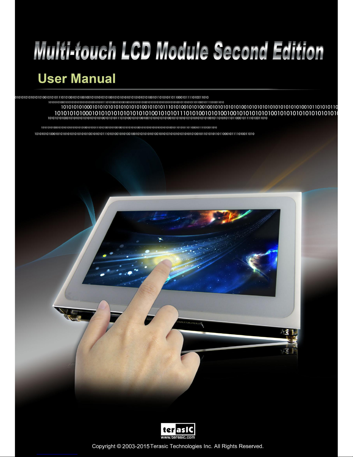
The MTL2 kit comes with the following contents:
Multi-touch LCD Module Second Edition
IDE Cable with ITG Adapter
5V Power Supply
Four Silicon Footstands
Users can download MTL2 system CD form http://cd-mtl2.terasic.com. The system CD contains
technical documents of the MTL2 kit, which includes component datasheets, demonstrations,
schematic, cable and user manual.
Figure 1-1 shows the contents of MTL2 kit.
Page 5
MLT2 User Manual
4
www.terasic.com
April 12, 2016
Figure 1-1 Contents of MTL2 Kit
11..2
2
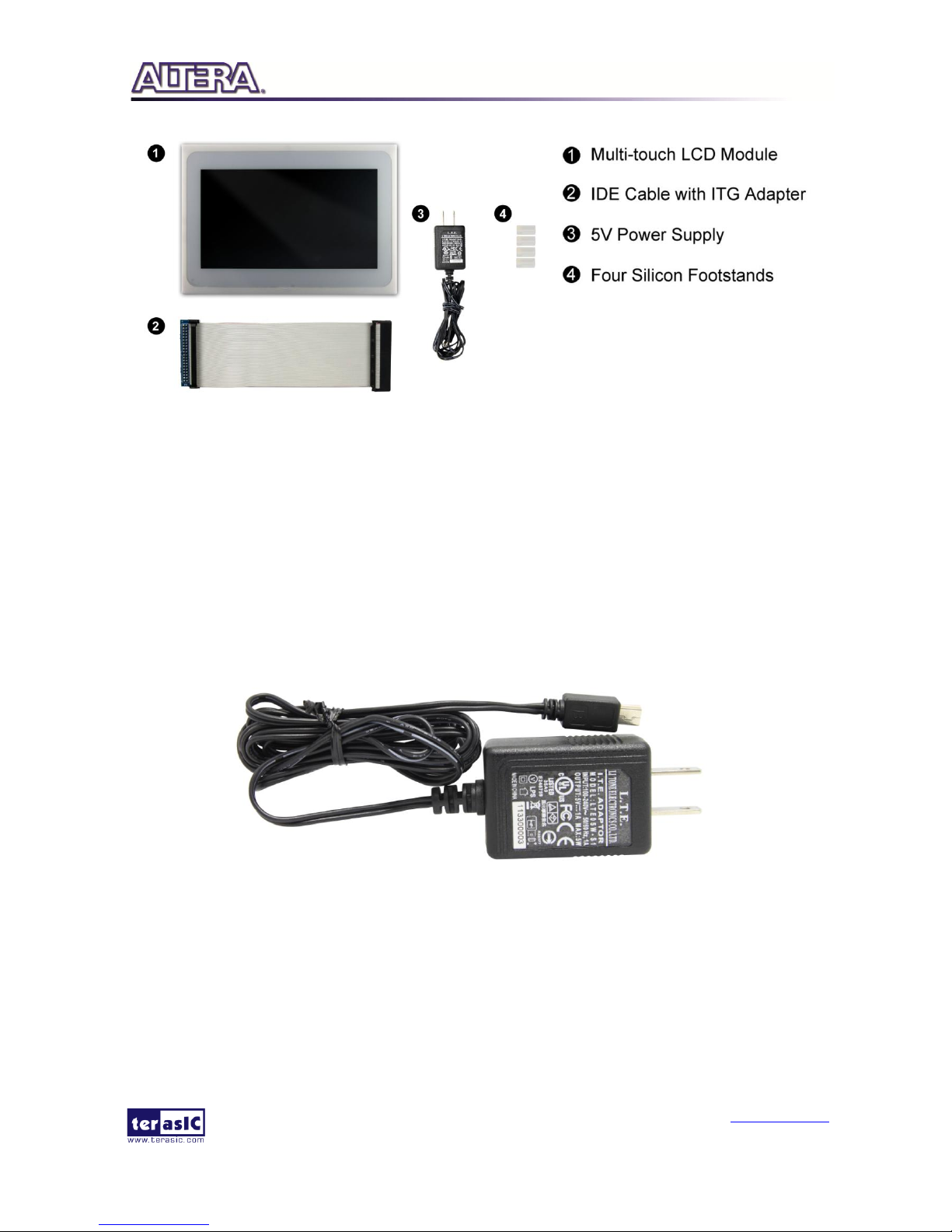
EExxtteerrnnaall PPoowweerr SSuuppppllyy ffoorr MMTTLL22
Figure 1-2 shows the power adapter for the MTL2. Due to the fact that the LCD panel in the
MTL may consumes more power than some FPGA boards can provide. a dedicated power adapter
for MTL2 is required as shown in Figure 1-3.
Figure 1-2 MTL2 Power Adapter
Page 6
MLT2 User Manual
5
www.terasic.com
April 12, 2016
Figure 1-3 External USB Power Connection Setup
11..3
3
AAsssseemmbbllyy
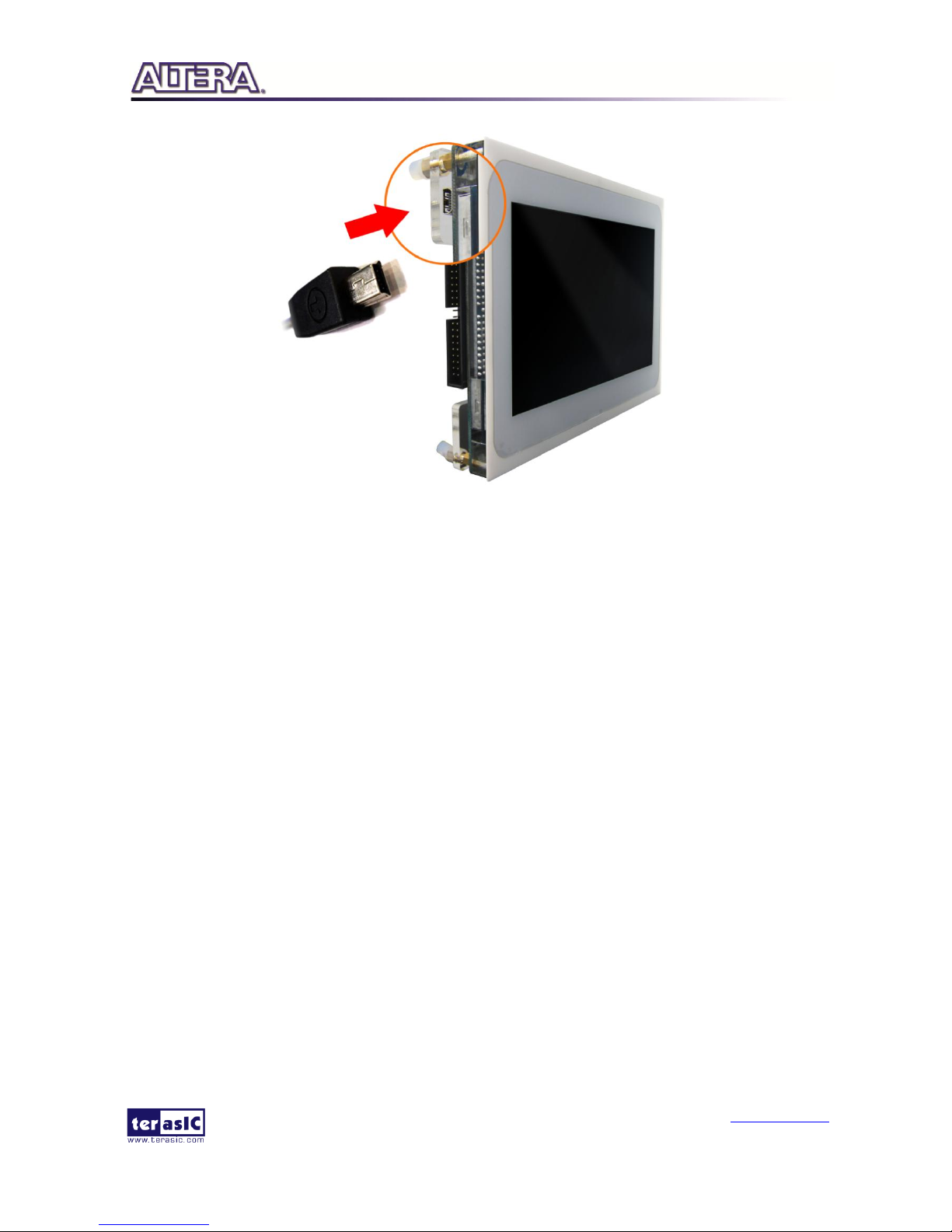
Here are the procedures to assemble the MTL2 kit:
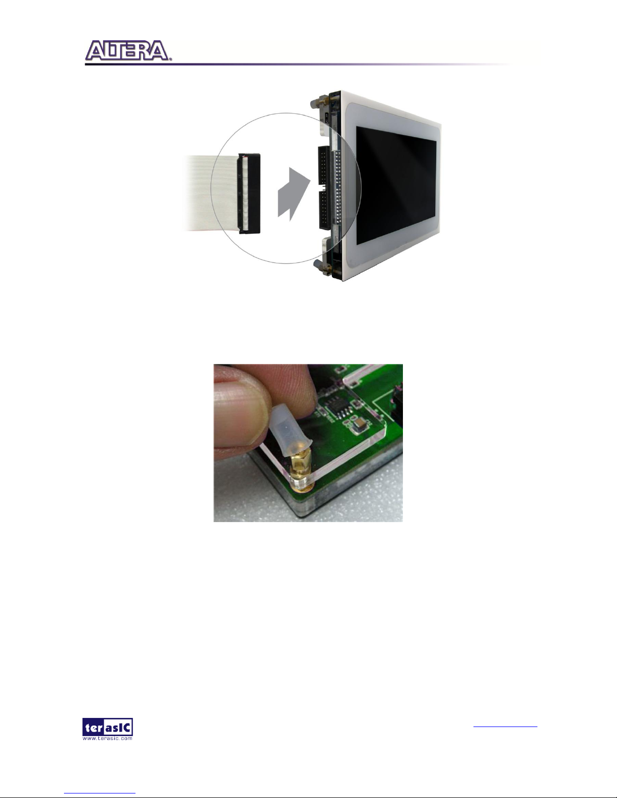
1. Connect the IDE cable to the IDE connector on the back of the MTL as shown in the Figure
1-4.
Page 7
MLT2 User Manual
6
www.terasic.com
April 12, 2016
Figure 1-4 MTL connection for the IDE cable
2. Place four silicon footstands to foot pegs of the MTL2 as shown in Figure 1-5.
Figure 1-5 MTL2 Footstand Setup
11..4
4
CCoonnnneeccttiivviittyy
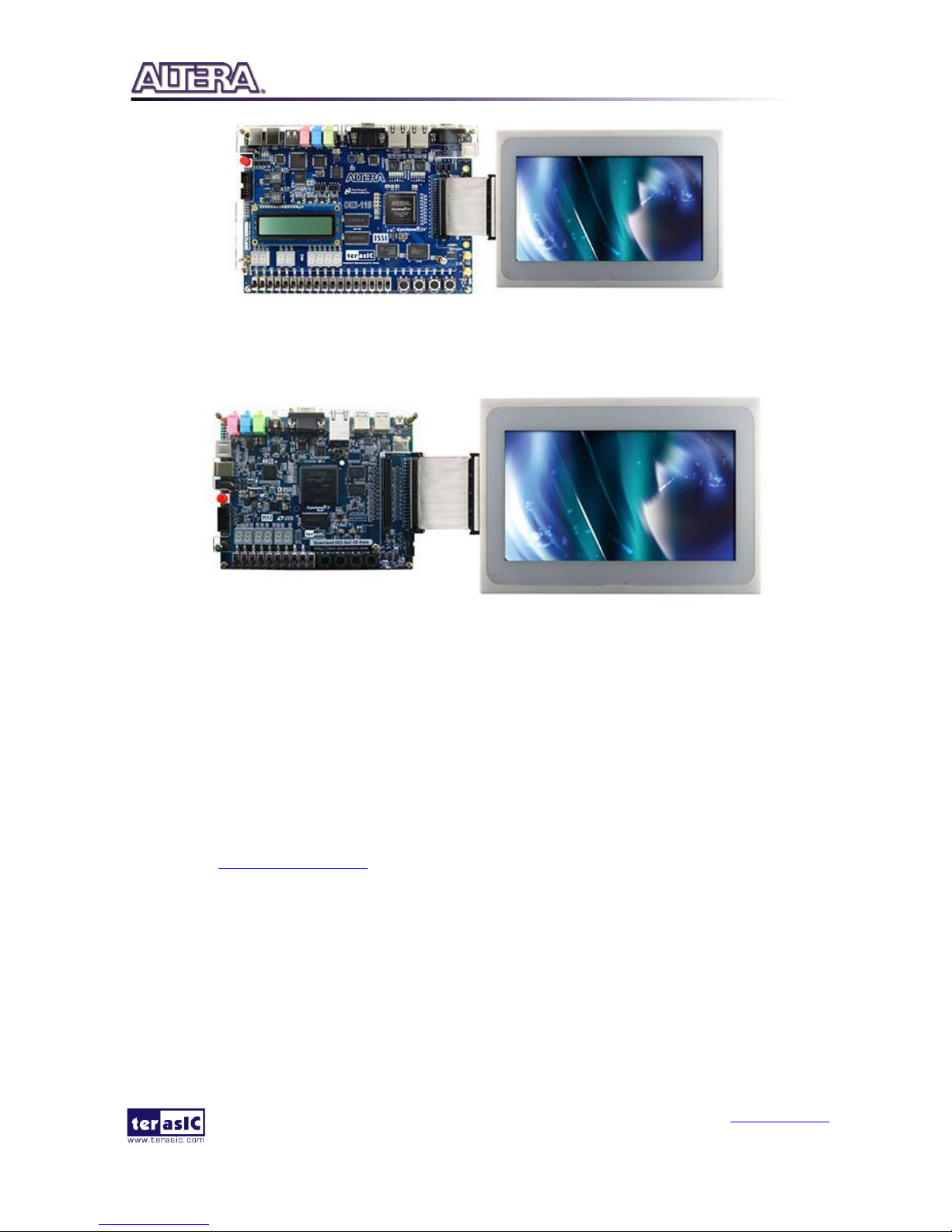
The following figures show the connectivity for MTL2 to DE2-115 and DE1-SoC FPGA
Development Boards.
Page 8
MLT2 User Manual
7
www.terasic.com
April 12, 2016
Figure 1-6 MTL2 with DE2-115
Figure 1-7 MTL2 with DE1-SoC
11..5
5
GGeettttiinngg HHeellpp
Here is information of how to get help if you encounter any problem:
Office Hours: 9:00 a.m. to 6:00 p.m. (GMT +8)
Telephone: +886-3-550-8800
Email: support@terasic.com
Page 9

MLT2 User Manual
8
www.terasic.com
April 12, 2016
Chapter 2
Architecture of MTL2
This chapter provides information regarding features and architecture of the MTL2.
22..1
1
FFeeaattuurreess
The key features of this module are listed below:
800x480 pixel resolution LCD with 24-bit color depth
Five-point touch support
Gesture support
IDE interface
2x20 GPIO interface with ITG adapter
22..2
2
MMTTLL22 KKiitt
The MTL2 kit is assembled via three components:
Multi-touch LCD Module
IDE Cable
IDE to GPIO (ITG) adapter
The IDE cable is used to provide a high-speed signal transmission for 33 MHz video signals. The
ITG adapter is designed to map the standard IDE pin assignment to the 2x20 GPIO interface on the
FPGA boards.
22..3
3
CCoommppoonneenntt aanndd LLaayyoouutt
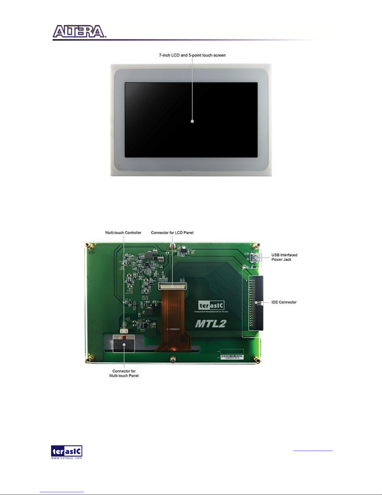
The top view of MTL2 is shown in Figure 2-1.
Page 10
MLT2 User Manual
9
www.terasic.com
April 12, 2016
Figure 2-1 MTL2 Top View
The bottom view of MTL2 is shown in Figure 2-2. It depicts the layout and indicates the locations
of connectors and key components.
Figure 2-2 MTL2 Bottom View
Page 11

MLT2 User Manual
10
www.terasic.com
April 12, 2016
BBlloocckk DDiiaaggrraamm
Figure 2-3 shows the block diagram of MTL2. The IDE connector houses all the wires from
peripheral interfaces, connecting to the FPGA of a development kit through the IDE cable and ITG
adapter.
Figure 2-3 Block Diagram of MTL2
Figure 2-4 illustrates the connection for MTL2 to the Terasic FPGA boards.
Figure 2-4 Connection Diagram of MTL2 Kit with Terasic FPGA boards
Page 12

MLT2 User Manual
11
www.terasic.com
April 12, 2016
22..4
4
IIDDEE CCaabbllee
The connection cable included is a standard IDE cable. However, to achieve the best performance,
we strongly recommend users use the bundled IDE cable only. Third-party IDE cables may cause
the MTL2 to malfunction, or even damage the module. The IDE cable is shown in Figure 2-5.
Figure 2-5 IDE cable
22..5
5
IITTGG AAddaapptteerr
The IDE to GPIO (ITG) adapter is designed to remap IDE pins to GPIO pins.
Figure 2-6 and Figure 2-7 show the top view and bottom view of ITG adapter, respectively.
The J1 connector is used to connect the FPGA board. The J2 connector is used to interface with the
IDE cable.
Page 13

MLT2 User Manual
12
www.terasic.com
April 12, 2016
Figure 2-6 ITG Adapter (Top View)
Figure 2-7 ITG Adapter (Bottom View)
Page 14

MLT2 User Manual
13
www.terasic.com
April 12, 2016
Chapter 3
Using the MTL2
This chapter provides information on how to control the MTL2 hardware, including definition of
2x20 GPIO interface, LCD control, and multi-touch control signals.
33..1
1
PPiinn DDeeffiinniittiioonn ooff 22xx2200 GGPPIIOO CCoonnnneeccttoorr
The 2x20 GPIO female connector is designed to directly connect to the 2x20 GPIO male connector
on the Terasic FPGA development boards. Figure 3-1 shows the signal names of the 2x20 GPIO
from the ITG adapter.
Figure 3-1 2x20 GPIO
Table 3-1 shows the recommended pin assignments for the 2x20 GPIO pins in Quartus II.
Page 15

MLT2 User Manual
14
www.terasic.com
April 12, 2016
Table 3-1 Recommended Pin Assignments of 2x20 GPIO in Quartus II
Pin
Numbers
Pin Name
Direction
IO Standard
1
- - - 2 MTL_DCLK
Output
3.3-V LVTTL
3
- - - 4 MTL_R[0]
Output
3.3-V LVTTL
5
MTL_R[1]
Output
3.3-V LVTTL
6
MTL_R[2]
Output
3.3-V LVTTL
7
MTL_R[3]
Output
3.3-V LVTTL
8
MTL_R[4]
Output
3.3-V LVTTL
9
MTL_R[5]
Output
3.3-V LVTTL
10
MTL_R[6]
Output
3.3-V LVTTL
11 - - - 12 - - - 13
MTL_R[7]
Output
3.3-V LVTTL
14
MTL_G[0]
Output
3.3-V LVTTL
15
MTL_G[1]
Output
3.3-V LVTTL
16
MTL_G[2]
Output
3.3-V LVTTL
17
MTL_G[3]
Output
3.3-V LVTTL
18
MTL_G[4]
Output
3.3-V LVTTL
19 - - - 20 - - - 21
MTL_G[5]
Output
3.3-V LVTTL
22
MTL_G[6]
Output
3.3-V LVTTL
23
MTL_B[0]
Output
3.3-V LVTTL
24
MTL_G[7]
Output
3.3-V LVTTL
25
MTL_B[1]
Output
3.3-V LVTTL
26
MTL_B[2]
Output
3.3-V LVTTL
27
MTL_B[3]
Output
3.3-V LVTTL
28
MTL_B[4]
Output
3.3-V LVTTL
29 - - - 30 - - - 31
MTL_B[5]
Output
3.3-V LVTTL
32
MTL_B[6]
Output
3.3-V LVTTL
33
MTL_B[7]
Output
3.3-V LVTTL
34 - - - 35
MTL_HSD
Output
3.3-V LVTTL
36
MTL_VSD
Output
3.3-V LVTTL
37
MTL_TOUCH_I2C_SCL
Output
3.3-V LVTTL
Page 16

MLT2 User Manual
15
www.terasic.com
April 12, 2016
38
MTL_TOUCH_I2C_SDA
Inout
3.3-V LVTTL
39
MTL_TOUCH_INT_n
Input
3.3-V LVTTL
40 - -
-
33..2
2
UUssiinngg LLCCDD
The LCD features 800x480 pixel resolution and runs at 33 MHz pixel rate. There is no
configuration required to drive the LCD. The timing specification is defined as in the Table 3-2,
Table 3-3, Figure 3-2 and Figure 3-3.
Table 3-2 LCD Horizontal Timing Specifications
Item
Symbol
Typical Value
Unit
Min.
Typ.
Max.
Horizontal Display Area
thd - 800
-
DCLK
DCLK Frequency
fclk
26.4
33.3
46.8
MHz
One Horizontal Line
th
862
1056
1200
DCLK
HS pulse width
thpw 1
40
DCLK
HS Blanking
thb
46
46
46
DCLK
HS Front Porch
thfp
16
210
354
DCLK
Table 3-3 LCD Vertical Timing Specifications
Item
Symbol
Typical Value
Unit
Min.
Typ.
Max.
Vertical Display Area
tvd - 480
-
TH
VS period time
tv
510
525
650
TH
VS pulse width
tvpw 1 -
20
TH
VS Blanking
tvb
23
23
23
TH
HS Front Porch
tvfp 7 22
147
TH
Page 17

MLT2 User Manual
16
www.terasic.com
April 12, 2016
Figure 3-2 Horizontal input timing waveform
Figure 3-3 Vertical input timing waveform
33..3
3
UUssiinngg TTeerraassiicc MMuullttii--ttoouucchh IIPP
Terasic Multi-touch IP is provided for developers to retrieve user inputs, including multi-touch
gestures and single-touch. The file name of this IP is i2c_touch_config.v, which is located in
System CD \IP folder.
The IP decodes I2C information and outputs coordinates and gesture information. The inputs and
outputs of this IP module is shown below
Page 18

MLT2 User Manual
17
www.terasic.com
April 12, 2016
The purpose of signals for this IP is described in Table 3-4. The IP requires a 50 MHz signal as a
reference clock to the iCLK pin and system reset signal to the iRSTN. INT_n, The signals of
I2C_SCLK, and I2C_SDAT pins should be connected to the MTL_TOUCH_INT_n,
MTL_TOUCH_I2C_SCL, and MTL_TOUCH_I2C_SDA signals in the 2x20 GPIO header,
respectively.
When touch activity occurs, the control application should check whether the value of
oREG_GESTURE matches a pre-defined gesture ID defined in Table 3-4 and the relative X/Y
coordinates can be derived from oREG_X and oREG_Y. Figure 3-1 shows the signaltap II
waveform of the IP. When the oREADY rises, it indicates touch activity, and the associated
information can be collected from the oREG_X1~ oREG_X5, oREG_Y1~ oREG_Y5,
oREG_TOUCH_COUNT, and oREG_GESTURE pins.
Figure 3-4 Signaltap II Waveform for Multi-Touch IP
Page 19

MLT2 User Manual
18
www.terasic.com
April 12, 2016
Table 3-4 Definition of Terasic Multi-touch IP Signals
Pin Name
Direction
Description
iCLK
Input
Connect to 50MHz clock
iRSTN
Input
Connect to system reset signal
INT_n
Input
Connect to interrupt pin of touch IC
oREADY
Output
Triggered when the data of following six
outputs are valid
oREG_X1
Output
10-bit X coordinate of first touch point
oREG_Y1
Output
9-bit Y coordinate of first touch point
oREG_X2
Output
10-bit X coordinate of second touch point
oREG_Y2
Output
9-bit Y coordinate of second touch point
oREG_X3
Output
10-bit X coordinate of first touch point
oREG_Y3
Output
9-bit Y coordinate of second touch point
oREG_X4
Output
10-bit X coordinate of first touch point
oREG_Y4
Output
9-bit Y coordinate of second touch point
oREG_X5
Output
10-bit X coordinate of first touch point
oREG_Y5
Output
9-bit Y coordinate of second touch point
oREG_TOUCH_COUNT
Output
2-bit touch count. Valid value is 0, 1, or 2.
oREG_GESTURE
Output
8-bit gesture ID (See Table 3-5)
I2C_SCLK
Output
Connect to I2C clock pin of touch IC
I2C_SDAT
Inout
Connect to I2C data pin of touch IC
The gestures and IDs supported are shown in Table 3-5.
Page 20

MLT2 User Manual
19
www.terasic.com
April 12, 2016
Table 3-5 Gestures and Its IDs
Gesture
ID (hex)
Move Up
0x10
Move Left
0x14
Move Down
0x18
Move Right
0x1C
Zoom In
0x48
Zoom Out
0x49
No Gesture
0x00
Note: The Terasic IP Multi-touch IP can also be found under the \IP folder in the system CD, as well
as the reference designs.
Page 21

MLT2 User Manual
20
www.terasic.com
April 12, 2016
Chapter 4
ePhoto Demonstration
This chapter describes how to use MTL2 to design a simple HDL code to implement a photo viewer.
The demonstration can support the following Terasic FPGA boards:
DE2-115
44..1
1
OOppeerraattiioonn DDeessccrriippttiioonn
This demonstration implements a simple photo viewer. Before running this demonstration, three
800x480 photos should be vertically merged into one 800x1440 photo and be stored in FLASH of
the FPGA board in advance. In this demonstration, users can browse each photo by using single
touch "move right" or "move left" gesture to select the previous or next photo, as shown in Figure
4-1..
Figure 4-1 Select Next Photo by East Gesture
Also, users can use two-point zoom-in and zoom-out gestures to zoom the photo displayed, as
shown in Figure 4-2.
Page 22

MLT2 User Manual
21
www.terasic.com
April 12, 2016
Figure 4-2 Zoom-in using Zoom-in Gesture
44..2
2
BBlloocckk DDiiaaggrraamm ooff tthhee eePPhhoottoo DDeessiiggnn
This section describes the block diagram of the ePhoto demonstration to give users a better
understanding of the code provided.
Figure 4-3 shows the block diagram of the ePhoto demonstration. When the demonstration starts up,
the system will control the Flash Controller to read the RGB data of three photos stored in the
FLASH, and write the data into SDRAM by using the writing port of the SDRAM. The SDRAM
Controller provides two reading ports and two writing ports. In this demonstration, only one
reading port and one write porting are used. To display the selected photo on the 800x480 LCD, the
VGA Controller will retrieve the photo data via reading the port of the SDRAM, and drive the LCD
display with the retrieved photo data. The VGA Controller retrieves the photo data at a rate of 60
photos per second. Zoom handles the photo zooming process. The displayed photo is zoomed
before being sent to the LCD display.
When users touch the MTL2 screen, I2C Touch Config will receive an interrupt signal from the
touch screen. When an interrupt is detected, I2C Touch Config will read touch information from the
touch panel and assert the oREADY signal. When Touch Controller detects a rising signal of
oREADY, it will read touch information and determine the input, which may be a gesture or a
single-point touch. If a west or east gesture is detected, it will change the reading port address of the
desired active photo in the SDRAM Controller. If a zoom-in or zoom-out gesture is detected, it will
change the zooming factor in Zoom.
For multi-touch gesture processing, a Terasic Memory-Mapped IP I2C_Touch_Config is used to
retrieve the touch information. For IP-usage details, please refer to the Chapter 3 in this document.
Note: the IP is encrypted, so the license should be installed before compiling the Quartus II project.
Page 23

MLT2 User Manual
22
www.terasic.com
April 12, 2016
Figure 4-3 The Block Diagram of the ePhoto Demonstration
44..3
3
LLooaaddiinngg PPhhoottooss iinnttoo FFLLAASSHH
Before executing the demonstration, users have to utilize the Control Panel software to load photos
into the FLASH of the FPGA board first. The Control Panel software is available in the CD of the
FPGA development kit.
Procedure for loading photos to FLASH:
1. Make sure the USB-Blaster download cable is connected to the host PC.
2. Power on the FPGA Development Board.
3. Execute the Control Panel application software. Please refer to the user manual of the FPGA
development kit for more information for the Control Panel software.
4. Switch to the FLASH page and click on the “Chip Erase (xx Sec)” button to erase FLASH
data.
5. Click on the “File Length” checkbox to indicate that you want to load the entire file.
6. Click on the “Write a File to FLASH” button. When the Control Panel responds with the
standard Windows dialog box and asks for the source file, select the “DEMO.raw” file in the
“Demonstrations\RTL\Photo” directory
7. When loading is completed, a prompt will appear indicating success.
Page 24

MLT2 User Manual
23
www.terasic.com
April 12, 2016
44..4
4
DDeemmoonnssttrraattiioonn ffoorr TTeerraassiicc DDEE22--111155 FFPPGGAA BBooaarrdd
This section shows how to setup the painter demo on the Terasic DE2-115 FPGA Board. For other
Terasic FPGA boards, the setup procedures are similar.
HHaarrddwwaarree SSeettuupp
The demonstration configuration is as shown in FFiigguurree 44--44.. Make sure the ITG adapter is
connected firmly to the IDE cable. Plug the ITG adapter into the GPIO-0 header of the FPGA
development kit from MTL2 before turning on. Important: Plug the MTL2 power adaptor into the
power connector of MTL2 unless the DE2-115 FPGA board is used.
Figure 4-4 DE2-115 ePhoto Configuration Setup
EExxeeccuuttee DDeemmoonnssttrraattiioonn
Procedure to execute demonstration:
1. Make sure the DE2-115 is powered off.
2. Mount the ITG adapter onto the 2x20 GPIO 0 expansion header of the DE2-115.
3. Connect the DE2-115 USB-Blaster USB port to the PC USB Port with a USB Cable.
4. Power on the DE2-115 FPGA Development Board.
5. Make sure Quartus II 13.1 and NIOS II 13.1 are installed in your system.
6. If you haven’t already, store pictures into the flash memory. For more detailed instructions
please refer to section 4.3 Loading Photos into FLASH.
7. Copy the folder Demonstrations\RTL\DE2_115_MTL2_EPHOTO\demo_batch in the MTL2
System CD onto your system and execute “test.bat”.
8. A photo should be displayed in the LCD, as shown in FFiigguurree 44--55.
9. Slide left or right with one finger on the touch panel to display the previous and next photos
Page 25

MLT2 User Manual
24
www.terasic.com
April 12, 2016
respectively.
10. Slide with two fingers in the opposite direction to zoom-in on the picture and pinch two
fingers together to zoom the picture out.
Figure 4-5 Photo Display
44..5
5
CCuussttoomm DDiissppllaayy PPhhoottoo
Procedure for creating custom photos for ePhoto:
1. Prepare three 24-bit bitmap format photos with image resolutions of 800 (width) x 480 (height)
pixels for each, as shown in Figure 4-6.
Figure 4-6 Original Photo Resolution
Page 26

MLT2 User Manual
25
www.terasic.com
April 12, 2016
2. Use image processing software to vertically merge the three photos into a new photo image with
24-bits color bitmap format. The merged photo resolution should be 800 (width) x 1440 (height)
pixels, as shown in Figure 4-7.
3. Use the tool “bmp_to_raw.exe” in the “Demonstrations\RTL\Photo” directory to convert the
picture to raw file. This tool will removing bmp file header that help flash controller read the
correct file data.
Figure 4-7 Photo Format for the ePhoto Demonstration
Page 27

MLT2 User Manual
26
www.terasic.com
April 12, 2016
Chapter 5
Painter Demonstration
This chapter shows how to implement a painter demo on the Multi-Touch LCD Module based on
SOPC Builder and the Altera’s Video and Image Processing Suite (VIP). The design demonstrates
how to use multi-touch gestures and single-touch. The demonstration requires the following
hardware:
Terasic FPGA Board
Multi-touch LCD Module
55..1
1
OOppeerraattiioonn DDeessccrriippttiioonn
Figure 5-1 shows the Graphical User Interface (GUI) of the Painter Demo. The GUI is classified
into four separate areas: Painting Area, Gesture Indicator, Clear Button, and Color Palette. Users
can select a pen color from the color palette and start painting in the paint area. To clear the painting
area, click the “Clear” button.
Figure 5-1 GUI of Painter Demo
Page 28

MLT2 User Manual
27
www.terasic.com
April 12, 2016
Figure 5-2 displays the five-finger painting of the canvas area.
Figure 5-2 Five-finger Painting
55..2
2
SSyysstteemm DDeessccrriippttiioonn
For LCD display processing, the reference design is developed based on Altera’s Video and Image
Processing Suite (VIP). The Frame Reader VIP is used for reading display content from the
associated video memory, and VIP Video Out is used to display the display content. The display
content is drawn by the NIOS II processor according to user input.
For multi-touch processing, a Terasic Memory-Mapped IP is used to retrieve the user input,
including multi-touch gestures and single-touch coordinates. For IP--usage details please refer to
the Chapter Three in this document. Note: the IP is encrypted, so the license should be installed
before compiling the Quartus II project.
Figure 5-3 shows the system generic block diagram of demonstration reference design.
Page 29

MLT2 User Manual
28
www.terasic.com
April 12, 2016
Figure 5-3 System Block Diagram
55..3
3
DDeemmoonnssttrraattiioonn ffoorr TTeerraassiicc DDEE22--111155 FFPPGGAA BBooaarrdd
This section shows how to setup the painter demo on the Terasic DE2-115 FPGA Board. For other
Terasic FPGA boards, the setup procedures are similar.
HHaarrddwwaarree SSeettuupp
Figure 5-4 Hardware Setup with DE2-115
Page 30

MLT2 User Manual
29
www.terasic.com
April 12, 2016
Figure 5-5 Hardware Setup with DE1-SoC
Figure 5-6 Hardware Setup with DE0-Nano
Figure 5-7 Hardware Setup with DE0-CV
Page 31

MLT2 User Manual
30
www.terasic.com
April 12, 2016
Figure 5-8 Hardware Setup with DE2-115
EExxeeccuuttee DDeemmoonnssttrraattiioonn
Please follow the procedures below to setup the demonstration:
1. Make sure the DE2-115 is powered off.
2. Mount the ITG adapter onto the 2x20 GPIO 0 expansion header of the DE2-115.
3. Connect the DE2-115 USB-Blaster USB-B port to the PC USB Port with a USB Cable.
4. Power on the DE2-115 FPGA Development Board.
5. Make sure Quartus II 13.1 and NIOS II 13.1 are installed on your system.
6. Copy the folder Demonstrations/Qsys/DE2_115_MTL2_PAINTER/demo_batch in the MTL
System CD onto your system and execute “test.bat”.
7. Now, you should see the painter GUI on the LCD.
5.4
DDeemmoonnssttrraattiioonn SSoouurrccee CCoodde
e
The source code locations of this demonstration for the various Terasic FPGA boards are shown in
Table 5-1. Note: The project is built under Quartus II 13.1, and both Altera VIP license and Terasic
Multi-Touch IP license are required for rebuilding the project.
Table 5-1 Source Code Locations of Painter Demonstration
FPGA Board
Location
DE2
Demonstrations\Qsys\DE2_MTL2_PAINTER
DE2-115
Demonstrations\ Qsys \DE2_115_MTL2_PAINTER
DE1-SoC
Demonstrations\ Qsys \ DE1-SoC _MTL2_PAINTER
DE0-Nano
Demonstrations\ Qsys \ DE0-Nano _MTL2_PAINTER
DE0-CV
Demonstrations\ Qsys \DE0-CV _MTL2_PAINTER
Page 32

MLT2 User Manual
31
www.terasic.com
April 12, 2016
Chapter 6
Appendix
66..1
1
RReevviissiioonn HHiissttoorryy
Version
Change Log
V1.0
Initial Version (Preliminary)
V1.0.1
Modify Figure 5-2 Description
V1.0.2
Modify Figure 5-7
V1.0.3
Modify Figure 5-7 change DE0-nano-soc to DE0-nano
66..2
2
CCooppyyrriigghhtt SSttaatteemmeenntt
Copyright © 2016 Terasic Technologies. All rights reserved.
We will continue to provide interesting examples and labs on our MTL2 webpage. Please visit
mtl2.terasic.com for more information.
Page 33

Mouser Electronics
Authorized Distributor
Click to View Pricing, Inventory, Delivery & Lifecycle Information:
Terasic:
P0189
 Loading...