

Page 1
MAX 10 Plus User
Manual
1
www.terasic.com
May 31, 2019
Page 2

MAX 10 Plus User
Manual
2
www.terasic.com
May 31, 2019
CONTENTS
Chapter 1 MAX 10 Plus Development Kit ..................................................................4
1.1 Package Contents........................................................................................................................ 4
1.2 MAX 10 Plus System CD ........................................................................................................... 5
1.3 Getting Help ............................................................................................................................... 5
Chapter 2 Introduction of the MAX 10 Plus ...............................................................6
2.1 Layout and Components ............................................................................................................. 6
2.2 Block Diagram of the MAX 10 Plus .......................................................................................... 7
Chapter 3 Using the MAX 10 Plus .............................................................................10
3.1 Configuration of MAX 10 FPGA on MAX 10 Plus ................................................................. 10
3.2 Board Status Elements .............................................................................................................. 14
3.3 Clock Circuitry ......................................................................................................................... 15
3.4 Peripherals Connected to the FPGA ......................................................................................... 16
3.4.1 User Push-buttons, Switches, LEDs ...................................................................................... 16
3.4.2 7-segment Displays ................................................................................................................ 19
3.4.3 Power Monitor ....................................................................................................................... 20
3.4.4 2x6 TMD Expansion Header ................................................................................................. 21
3.4.5 24-bit Audio CODEC ............................................................................................................ 22
3.4.6 Two Analog Input SMA Connectors ..................................................................................... 23
3.4.7 DDR3 Memory ...................................................................................................................... 23
3.4.8 QSPI Flash ............................................................................................................................. 25
3.4.9 Ethernet .................................................................................................................................. 26
3.4.10 HDMI RX .............................................................................................................................. 28
3.4.11 2x10 ADC Header ................................................................................................................. 29
3.4.12 Potentiometer ......................................................................................................................... 30
3.4.13 On-board Microphone ............................................................................................................ 30
3.4.14 PS/2 Serial Port ...................................................................................................................... 30
Page 3

MAX 10 Plus User
Manual
3
www.terasic.com
May 31, 2019
3.4.15 Digital-to-Analog Converter (DAC) ...................................................................................... 31
3.4.16 UART to USB ........................................................................................................................ 32
3.4.17 Ambient Light Sensor ............................................................................................................ 33
3.4.18 Humidity and Temperature Sensor ........................................................................................ 33
3.4.19 Accelerometer Sensor ............................................................................................................ 34
3.4.20 Micro SD Card Socket ........................................................................................................... 35
3.4.21 Power Distribution System .................................................................................................... 35
Chapter 4 The MAX 10 Plus System Builder ...........................................................37
4.1 Introduction .............................................................................................................................. 37
4.2 General Design Flow ................................................................................................................ 37
4.3 Using MAX 10 Plus System Builder ........................................................................................ 38
Chapter 5 RTL Example Codes .................................................................................44
5.1 PS/2 Mouse Demonstration ...................................................................................................... 44
5.2 ADC Potentiometer .................................................................................................................. 46
5.3 DAC Demonstration ................................................................................................................. 48
5.4 ADC/MIC/LED Demonstration ................................................................................................ 51
Chapter 6 NIOS Based Example Codes ....................................................................54
6.1 Power Monitor .......................................................................................................................... 54
6.2 UART to USB Control LED ..................................................................................................... 58
6.3 SD Card Audio Demonstration ................................................................................................. 61
6.4 DDR3 SDRAM Test by Nios II ................................................................................................ 65
6.5 Ethernet Socket server .............................................................................................................. 68
6.6 Digital Accelerometer Demonstration ...................................................................................... 75
6.7 Humidity/Temperature Sensor .................................................................................................. 77
Chapter 7 Programming the Configuration Flash Memory ...................................79
7.1 Internal Configuration .............................................................................................................. 79
7.2 Using Dual Compressed Images............................................................................................... 81
7.3 Nios II Load In Single Boot Image .......................................................................................... 84
Page 4
MAX 10 Plus User
Manual
4
www.terasic.com
May 31, 2019
Chapter 1
MAX 10 Plus Development Kit
The MAX 10 Plus board from Terasic is a full featured embedded evaluation kit based upon the
MAX10 family of Intel FPGAs. It offers a comprehensive design environment with everything
embedded developers need to create a processing-based system.
The MAX 10 Plus board delivers an integrated platform that includes hardware, design tools,
intellectual property and reference designs for developing a wide range of audio, video and many
other exciting applications.
The fully integrated kit allows developers to rapidly customize their processor and IP to suit their
specific needs, rather than constraining their software around the fixed feature set of the processor.
The all-in-one embedded solution, the MAX 10 Plus, making the best use of the parallel nature of
FPGAs.
1.1 Package Contents
Figure 1-1 shows a photograph of the MAX 10 Plus board package.
Figure 1-1 The MAX 10 Plus Board Package Contents
The MAX 10 Plus board package includes:
1. MAX 10 Plus board
2. MAX 10 Plus Quick Start Guide
3. 5V DC power adapter
Page 5

MAX 10 Plus User
Manual
5
www.terasic.com
May 31, 2019
4. One USB cables (Type A to Mini-B) for USB control and FPGA programming and control
1.2 MAX 10 Plus System CD
The MAX 10 Plus System CD contains all the documents and supporting materials associated with
MAX 10 Plus, including the user manual, system builder, reference designs, and device datasheets.
Users can download this system CD from the link: http:// max10-plus.terasic.com/cd.
1.3 Getting Help
Here are the addresses where you can get help if you encounter any problems:
• Terasic Technologies
• 9F., No.176, Sec.2, Gongdao 5th Rd, East Dist, Hsinchu City, 30070. Taiwan
Email: support@terasic.com
Tel.: +886-3-575-0880
Website: max10-plus.terasic.com
Page 6
MAX 10 Plus User
Manual
6
www.terasic.com
May 31, 2019
Chapter 2
Introduction of the MAX 10 Plus
2.1 Layout and Components
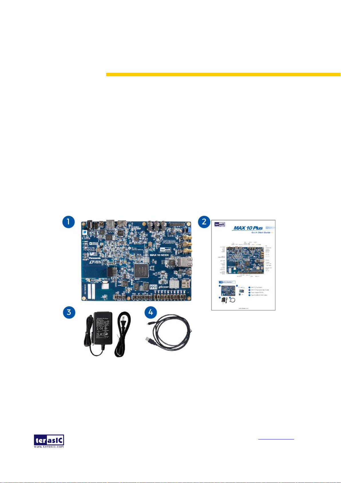
Figure 2-1 shows a photograph of the board. It depicts the layout of the board and indicates the
location of the connectors and key components.
Figure 2-1 MAX 10 Plus Development Board (top view)
The MAX 10 Plus board has many features that allow users to implement a wide range of designed
circuits, from simple circuits to various multimedia projects.
The following hardware is provided on the board:
• Intel MAX® 10 10M50DAF484C6G device
• USB-Blaster II onboard for programming; JTAG Mode
• 256MB DDR3 SDRAM (64Mx16 and 128Mx8)
• 64MB QSPI Flash
• Micro SD card socket
• Five push-buttons
• Ten slide switches
Page 7
MAX 10 Plus User
Manual
7
www.terasic.com
May 31, 2019
• Ten red user LEDs
• Two 7-segment displays
• Three 50MHz clock sources from the clock generator
• 24-bit CD-quality audio CODEC with line-in, line-out jacks
• On-board microphone
• HDMI RX, incorporates HDM v1.4a features, including 3D video supporting
• Gigabit Ethernet PHY with RJ45 connector
• UART to USB, USB Mini-B connector
• One ambient light sensor
• One humidity and temperature sensor
• One accelerometer
• One external 16bit digital-to-analog converter (DAC) device with SMA output
• Potentiometer input to ADC
• Two MAX 10 FPGA ADC SMA inputs
• One 2x10 ADC header with 16 analog inputs connected to MAX10 ADCs
2.2 Block Diagram of the MAX 10 Plus
Figure 2-2 is the block diagram of the board. All the connections are established through the MAX
10 FPGA device to provide maximum flexibility for users. Users can configure the FPGA to
implement any system design.
Figure 2-2 Block Diagram of MAX 10 Plus Board
Page 8

MAX 10 Plus User
Manual
8
www.terasic.com
May 31, 2019
FPGA Device
• MAX 10 10M50DAF484C6G Device
• Integrated dual ADCs, each ADC supports 1 dedicated analog input and 8 dual function pins
• 50K programmable logic elements
• 1,638Kbits embedded memory
• 5,888Kbits user flash memory
• 4 PLLs
Configuration and Debug
• On-board USB-Blaster II (Mini USB type B connector)
• Optional JTAG direct via 10-pin header
• One slide switch for dual boot image selection
Memory Device
• 256MB DDR3 SDRAM (64Mx16 and 128Mx8)
• 512MB QSPI Flash
• Micro SD card socket
Communication and Expansion Header
• Gigabit Ethernet PHY with RJ45 connector
• UART to USB, USB Mini-B connector
• PS/2 mouse/keyboard connector
• 2x6 TMD (Terasic Mini Digital) Expansion Header
Audio
• 24-bit CD-quality audio CODEC with line-in, line-out jacks
Video Input
• HDMI RX, incorporates HDM v1.4a features, including 3D video supporting
Analog
• Two MAX 10 FPGA ADC SMA inputs
• Potentiometer input to ADC
• On-Board MIC input to ADC
• 2x10 ADC header with 16 analog inputs connected to MAX10 ADCs
• One DAC SMA output
Switches, Buttons, and Indicators
• Five push-buttons
• Ten slide switches
Page 9

MAX 10 Plus User
Manual
9
www.terasic.com
May 31, 2019
• Ten red user LEDs
• Two 7-segment displays
Sensors
• Ambient light sensor
• Humidity and temperature sensor
• Accelerometer
• Power monitor
Power
• 5V/3A DC input
Page 10
MAX 10 Plus User
Manual
10
www.terasic.com
May 31, 2019
Chapter 3
Using the MAX 10 Plus
This chapter provides an instruction to use the board and describes the peripherals.
3.1 Configuration of MAX 10 FPGA on MAX 10 Plus
There are two types of configuration method supported by MAX 10 Plus:
1. JTAG configuration: configuration using JTAG port.
JTAG configuration scheme allows you to directly configure the device core through JTAG pins -
TDI, TDO, TMS, and TCK pins. The Quartus II software automatically generates .sof that is used
for JTAG configuration with a download cable in the Quartus II software programmer.
2. Internal configuration: configuration using internal flash.
Before internal configuration, you need to program the configuration data into the configuration
flash memory (CFM) which provides non-volatile storage for the bit stream. The information is
retained within CFM even if the MAX 10 Plus is turned off. When the board is powered on, the
configuration data in the CFM is automatically loaded into the MAX 10 FPGA.
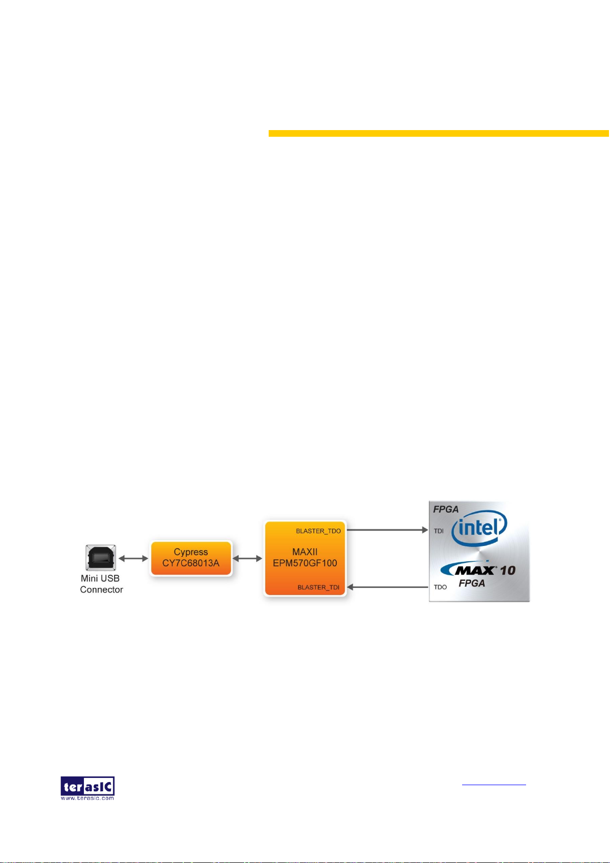
◼ JTAG Chain on MAX 10 Plus
The FPGA device can be configured through JTAG interface on MAX 10 Plus board, but the JTAG
chain must form a closed loop, which allows Quartus II programmer to the detect FPGA device.
Figure 3-1 illustrates the JTAG chain on MAX 10 Plus.
Figure 3-1 Path of the JTAG Chain
◼ Configure the FPGA in JTAG Mode
The following shows how the FPGA is programmed in JTAG mode step by step.
1. Open the Quartus II programmer and click Auto Detect, as circled in Figure 3-2.
Page 11

MAX 10 Plus User
Manual
11
www.terasic.com
May 31, 2019
Figure 3-2 Detect FPGA Device in JTAG Mode
2. Select detected device associated with the board, as circled in Figure 3-3.
Figure 3-3 Select 10M50DAES Device
3. FPGA is detected, as shown in Figure 3-4.
Page 12
MAX 10 Plus User
Manual
12
www.terasic.com
May 31, 2019
Figure 3-4 FPGA Detected in Quartus Programmer
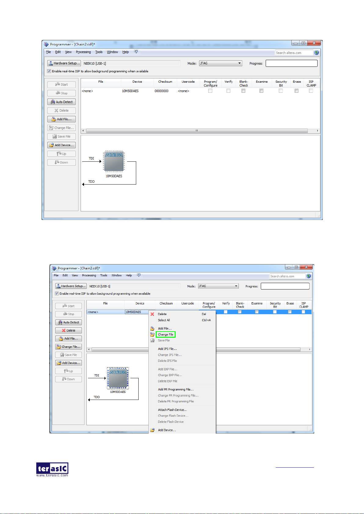
4. Right click on the FPGA device and open the .sof file to be programmed, as highlighted in
Figure 3-5.
Figure 3-5 Open the .sof File to be Programmed into the FPGA Device
Page 13
MAX 10 Plus User
Manual
13
www.terasic.com
May 31, 2019
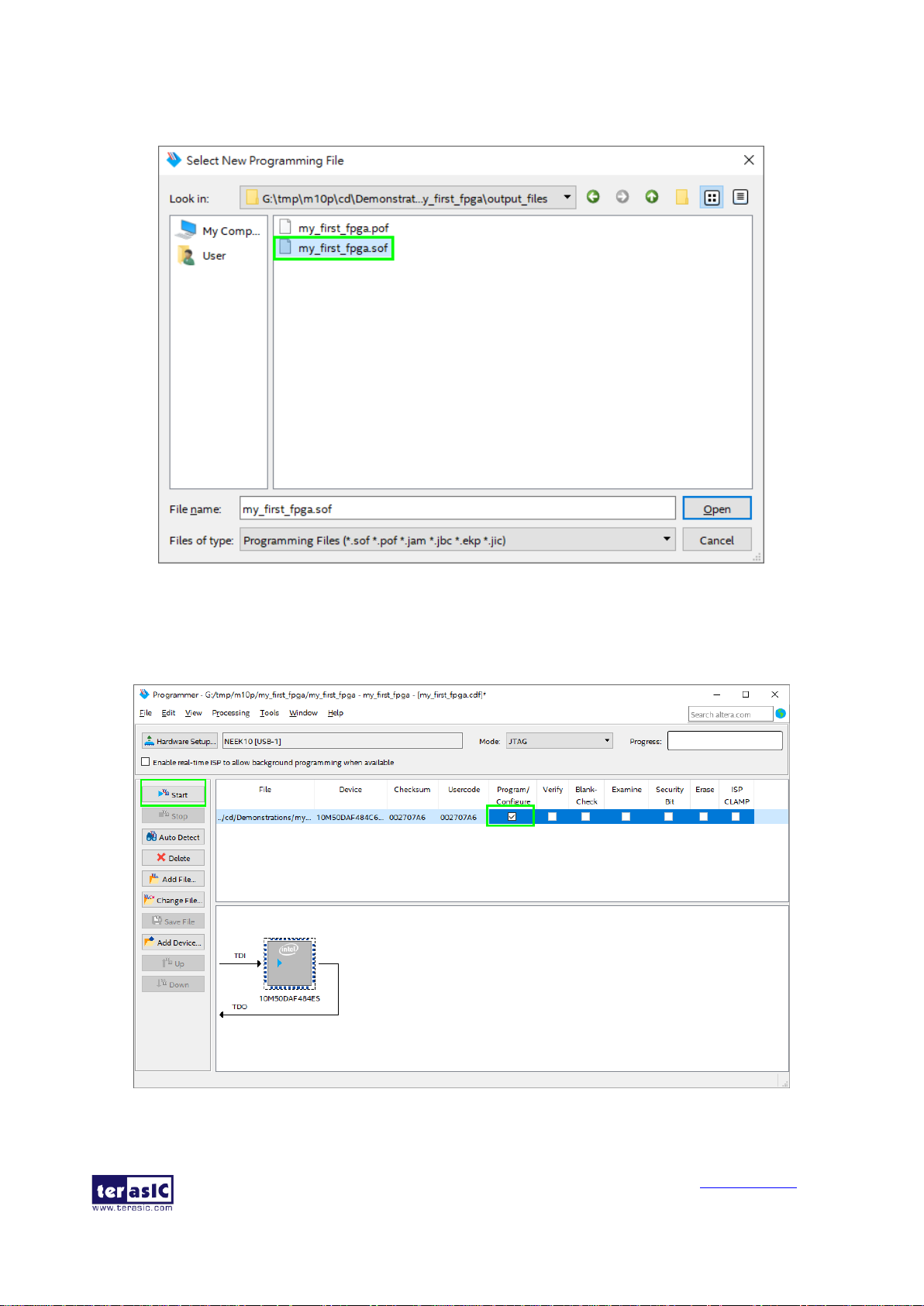
5. Select the .sof file to be programmed, as shown in Figure 3-6.
Figure 3-6 Select the .sof File to be Programmed into the FPGA Device
6. Click Program/Configure check box and then click Start button to download the .sof file
into the FPGA device, as shown in Figure 3-7.
Figure 3-7 Program. sof File into the FPGA Device
Page 14
MAX 10 Plus User
Manual
14
www.terasic.com
May 31, 2019
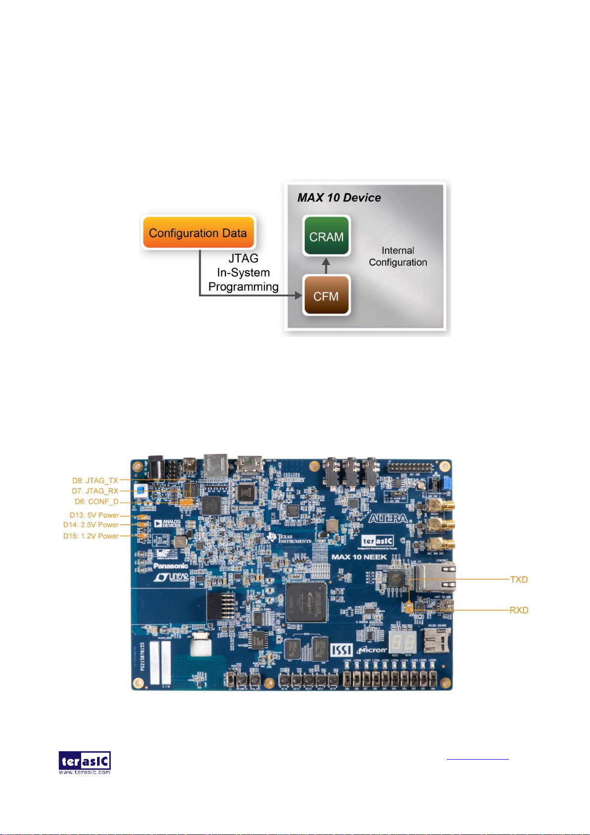
◼ Internal Configuration
• The configuration data to be written to CFM will be part of the programmer object file (.pof).
This configuration data is automatically loaded from the CFM into the MAX 10 devices when
the board is powered up.
• Please refer to Chapter 7 Programming the Configuration Flash Memory for the basic
programming instruction on the configuration flash memory (CFM).
Figure 3-8 High-Level Overview of Internal Configuration for MAX 10 Devices
3.2 Board Status Elements
In addition to the 10 LEDs that FPGA device can control, there are 4 indicators which can indicate
the board status (See Figure 3-9), please refer the details in Table 3-1.
Figure 3-9 LED Indicators on MAX 10 Plus
Page 15
MAX 10 Plus User
Manual
15
www.terasic.com
May 31, 2019
Table 3-1 LED Indicators
Board Reference
LED Name
Description
D13
5V Power
Illuminate when 5V power is active.
D14
2.5V Power
Illuminate when 2.5V power is active.
D16
1.2V Power
Illuminate when 1.2V power is active.
D6
CONF_DONE
Illuminate when configuration data is loaded into MAX 10 device
without error.
D7
JTAG_RX
Illuminate during data is uploaded from MAX 10 device to PC through
UB2.
D8
JTAG_TX
Illuminate during configuration data is loaded into MAX 10 device
from UB2.
TXD
TXD
Illuminate during transmitting data via USB.
RXD
RXD
Illuminate during receiving data via USB.
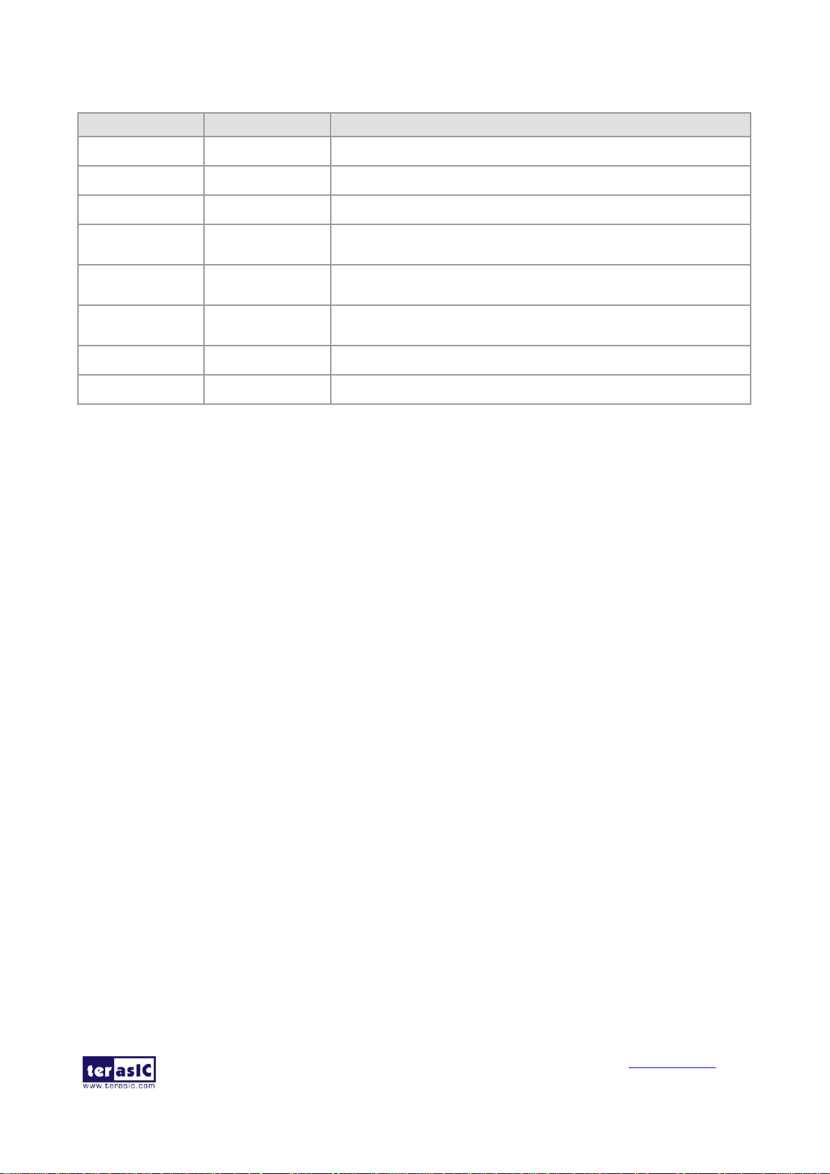
3.3 Clock Circuitry
Figure 3-10 shows the default frequency of all external clocks to the MAX 10 FPGA. A clock
generator is used to distribute clock signals with low jitter. The three 50MHz clock signals
connected to the FPGA are used as clock sources for user logic. One 25MHz clock signal is
connected to the clock input of Gigabit Ethernet Transceiver. One 24MHz clock signal is connected
to the clock inputs of USB microcontroller of USB Blaster II. One 28.63636MHz clock signal is
connected to the clock input of HDMI Receiver chip. The other 50MHz clock signal is connected to
MAX CPLD of USB Blaster II. One 10MHz clock signal is connected to the PLL1 and PLL3 of
FPGA, the outputs of these two PLLs can drive ADC clock. The associated pin assignment for
clock inputs to FPGA I/O pins is listed in Table 3-2.
Page 16
MAX 10 Plus User
Manual
16
www.terasic.com
May 31, 2019
Figure 3-10 Block Diagram of the Clock Distribution on MAX 10 Plus
Table 3-2 Pin Assignment of Clock Inputs
Signal Name
FPGA Pin No.
Description
I/O Standard
MAX10_CLK1_50
PIN_N5
50MHz clock input
2.5V
MAX10_CLK2_50
PIN_V9
50MHz clock input
3.3V
MAX10_CLK3_50
PIN_N14
50MHz clock input
1.5V
ADC_CLK_10
PIN_M9
10MHz clock input
3.3V
3.4 Peripherals Connected to the FPGA
This section describes the interfaces connected to the FPGA. User can control or monitor different
interfaces with user logic from the FPGA.
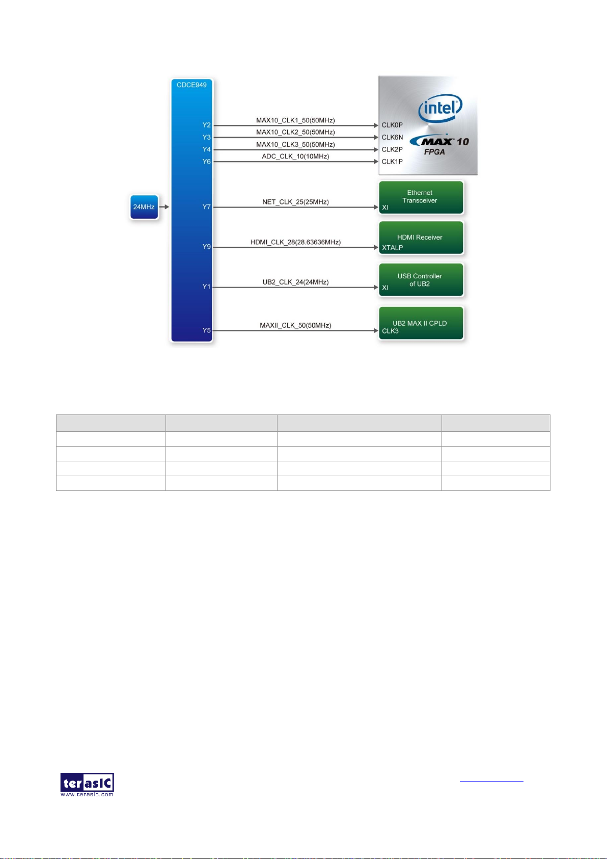
3.4.1 User Push-buttons, Switches, LEDs
The board has five push-buttons connected to the FPGA, as shown in Figure 3-11. MAX 10 devices
support Schmitt trigger input on all I/O pins. A Schmitt trigger feature introduces hysteresis to the
input signal for improved noise immunity, especially for signal with slow edge rate and act as
switch debounce in Figure 3-12 for the push-buttons connected.
Page 17
MAX 10 Plus User
Manual
17
www.terasic.com
May 31, 2019
Figure 3-11 Connections between the Push-buttons and the MAX 10 FPGA
Figure 3-12 Switch Debouncing
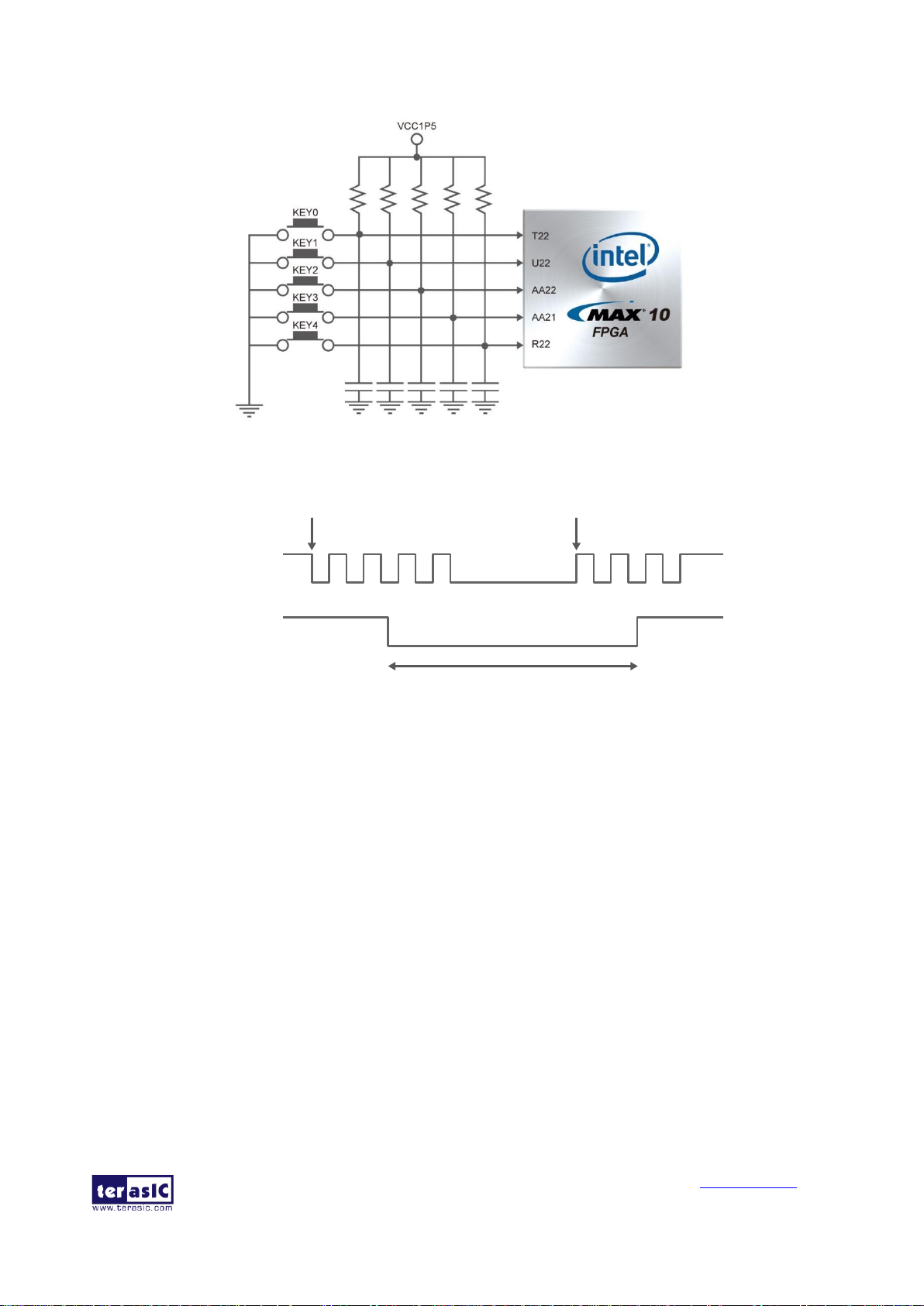
There are two ten switches connected to the FPGA, as shown in Figure 3-13. These switches are
used as level-sensitive data inputs to a circuit. Each switch is connected directly and individually to
the FPGA. When the switch is set to the DOWN position (towards the edge of the board), it
generates a low logic level to the FPGA. When the switch is set to the UP position, a high logic
level is generated to the FPGA.
Pushbutton releasedPushbutton depressed
Before
Debouncing
Schmitt Trigger
Debounced
Page 18
MAX 10 Plus User
Manual
18
www.terasic.com
May 31, 2019
Figure 3-13 Connections between the Slide Switches and the MAX 10 FPGA
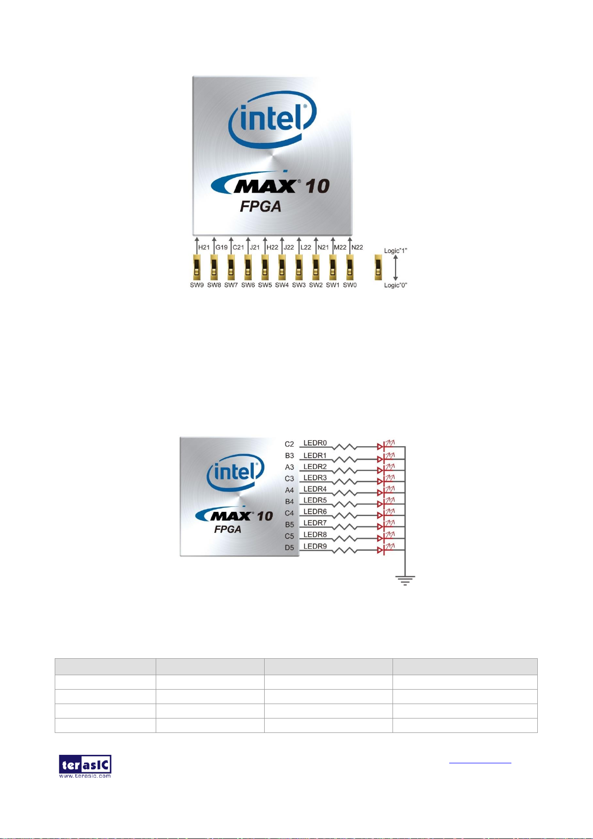
There are also ten user-controllable LEDs connected to the FPGA. Each LED is driven directly and
individually by the MAX 10 FPGA; driving its associated pin to a high logic level or low level to
turn the LED on or off, respectively. Figure 3-14 shows the connections between LEDs and MAX
10 FPGA. Table 3-3, Table 3-4 and Table 3-5 list the pin assignment of user push-buttons, switches,
and LEDs.
Figure 3-14 Connections between the LEDs and the MAX 10 FPGA
Table 3-3 Pin Assignment of Push-buttons
Signal Name
FPGA Pin No.
Description
I/O Standard
KEY[0]
PIN_T22
Push-button[0]
1.5V
KEY[1]
PIN_U22
Push-button[1]
1.5V
KEY[2]
PIN_AA22
Push-button[2]
1.5V
KEY[3]
PIN_AA21
Push-button[3]
1.5V
Page 19
MAX 10 Plus User
Manual
19
www.terasic.com
May 31, 2019
KEY[4]
PIN_R22
Push-button[4]
1.5V
Table 3-4 Pin Assignment of Slide Switches
Signal Name
FPGA Pin No.
Description
I/O Standard
SW[0]
PIN_N22
Slide Switch[0]
1.5V
SW[1]
PIN_M22
Slide Switch[1]
1.5V
SW[2]
PIN_N21
Slide Switch[2]
1.5V
SW[3]
PIN_L22
Slide Switch[3]
1.5V
SW[4]
PIN_J22
Slide Switch[4]
1.5V
SW[5]
PIN_H22
Slide Switch[5]
1.5V
SW[6]
PIN_J21
Slide Switch[6]
1.5V
SW[7]
PIN_C21
Slide Switch[7]
1.5V
SW[8]
PIN_G19
Slide Switch[8]
1.5V
SW[9]
PIN_H21
Slide Switch[9]
1.5V
Table 3-5 Pin Assignment of LEDs
Signal Name
FPGA Pin No.
Description
I/O Standard
LEDR[0]
PIN_C2
LEDR [0]
3.3V
LEDR[1]
PIN_B3
LEDR [1]
3.3V
LEDR[2]
PIN_A3
LEDR [2]
3.3V
LEDR[3]
PIN_C3
LEDR [3]
3.3V
LEDR[4]
PIN_A4
LEDR [4]
3.3V
LEDR[5]
PIN_B4
LEDR [5]
3.3V
LEDR[6]
PIN_C4
LEDR [6]
3.3V
LEDR[7]
PIN_B5
LEDR [7]
3.3V
LEDR[8]
PIN_C5
LEDR [8]
3.3V
LEDR[9]
PIN_D5
LEDR [9]
3.3V
3.4.2 7-segment Displays
The MAX 10 Plus has two 7-segment displays. These displays are paired to display numbers in
various sizes. Figure 3-15 shows the connection of seven segments (common anode) to pins on
MAX 10 FPGA. The segment can be turned on or off by applying a low logic level or high logic
level from the FPGA, respectively.
Each segment in a display is indexed from 0 to 6, with corresponding positions given in Figure
3-15. Table 3-6 shows the pin assignment of FPGA to the 7-segment displays.
Page 20
MAX 10 Plus User
Manual
20
www.terasic.com
May 31, 2019
Figure 3-15 Connections between the 7-segment Display HEX0 and the MAX 10 FPGA
Table 3-6 Pin Assignment of 7-segment Displays
Signal Name
FPGA Pin No.
Description
I/O Standard
HEX0[0]
PIN_D6
Seven Segment Digit 0[0]
3.3V
HEX0[1]
PIN_A5
Seven Segment Digit 0[1]
3.3V
HEX0[2]
PIN_C6
Seven Segment Digit 0[2]
3.3V
HEX0[3]
PIN_A6
Seven Segment Digit 0[3]
3.3V
HEX0[4]
PIN_F7
Seven Segment Digit 0[4]
3.3V
HEX0[5]
PIN_D7
Seven Segment Digit 0[5]
3.3V
HEX0[6]
PIN_B7
Seven Segment Digit 0[6]
3.3V
HEX1[0]
PIN_C7
Seven Segment Digit 1[0]
3.3V
HEX1[1]
PIN_C8
Seven Segment Digit 1[1]
3.3V
HEX1[2]
PIN_D8
Seven Segment Digit 1[2]
3.3V
HEX1[3]
PIN_D10
Seven Segment Digit 1[3]
3.3V
HEX1[4]
PIN_E10
Seven Segment Digit 1[4]
3.3V
HEX1[5]
PIN_H11
Seven Segment Digit 1[5]
3.3V
HEX1[6]
PIN_E6
Seven Segment Digit 1[6]
3.3V
3.4.3 Power Monitor
The MAX 10 Plus has implemented three power monitor chips to monitor the FPGA core power
and VCCIO power voltage and current. Figure 3-16 shows the connection between the power
monitor chip and the MAX 10 FPGA. Through the I2C serial interface, the power monitor can be
configured to measure remote voltage and remote current. Programmable calibration value,
conversion times, and averaging, combined with an internal multiplier, enable direct readouts of
current in amperes and power in watts. Table 3-7 shows the pin assignment of power monitor I2C
bus.
Page 21
MAX 10 Plus User
Manual
21
www.terasic.com
May 31, 2019
Figure 3-16 Connections between the Power Monitor Chip and the MAX 10 FPGA
Table 3-7 Pin Assignment of Power Monitor I2C Bus
Signal Name
FPGA Pin No.
Description
I/O Standard
PM_I2C_SCL
PIN_E8
Power Monitor SCL
3.3V
PM_I2C_SDA
PIN_E9
Power Monitor SDA
3.3V
3.4.4 2x6 TMD Expansion Header
The board has one 2x6 TMD (Terasic Mini Digital) expansion header. The TMD header has 8
digital GPIO user pins connected to the MAX 10 FPGA, two 3.3V power pins and two ground pins.
There are two Transient Voltage Suppressor diode arrays used to implement ESD protection for 8
GPIO user pins.
Figure 3-17 shows the connection between the TMD header and MAX 10 FPGA. Table 3-8 shows
the pin assignment of 2x6 TMD header.
Figure 3-17 Connections between the 2x6 TMD Header and MAX 10 FPGA
Page 22
MAX 10 Plus User
Manual
22
www.terasic.com
May 31, 2019
Table 3-8 Pin Assignment of 2x6 TMD Header
Signal Name
FPGA Pin No.
Description
I/O Standard
GPIO[0]
PIN_Y17
GPIO Connection [0]
3.3V
GPIO[1]
PIN_AA17
GPIO Connection [1]
3.3V
GPIO[2]
PIN_V16
GPIO Connection [2]
3.3V
GPIO[3]
PIN_W15
GPIO Connection [3]
3.3V
GPIO[4]
PIN_AB16
GPIO Connection [4]
3.3V
GPIO[5]
PIN_AA16
GPIO Connection [5]
3.3V
GPIO[6]
PIN_Y16
GPIO Connection [6]
3.3V
GPIO[7]
PIN_W16
GPIO Connection [7]
3.3V
3.4.5 24-bit Audio CODEC
The MAX 10 Plus offers high-quality 24-bit audio via the Texas Instruments TLV320AIC3254
audio CODEC (Encoder/Decoder). This chip on MAX 10 Plus supports, line-in, line-out and
microphone-in ports with adjustable sample rate from 8KHz to 192KHz. The connection of the
audio circuitry to the FPGA is shown in Figure 3-18, and the associated pin assignment to the
FPGA is listed in Table 3-9. More information about the TLV320AIC3254 CODEC is available in
its datasheet, which can be found on the manufacturer’s website, or in the directory
\Datasheet\Audio CODEC of MAX 10 Plus System CD.
Figure 3-18 Connections between the FPGA and Audio CODEC
Table 3-9 Pin Assignment of Audio CODEC
Signal Name
FPGA
Pin No.
Description
I/O
Standard
AUDIO_MCLK
PIN_J11
Master output Clock
2.5V
AUDIO_BCLK
PIN_J12
Audio serial data bus (primary) bit clock
2.5V
AUDIO_WCLK
PIN_H12
Audio serial data bus (primary) word clock
2.5V
AUDIO_DIN_MFP1
PIN_J13
Audio serial data bus data output/digital microphone output
2.5V
AUDIO_DOUT_MFP2
PIN_H13
Audio serial data bus data input/general purpose input
2.5V
AUDIO_SCLK_MFP3
PIN_H14
SPI serial Clock/headphone-detect output
2.5V
Page 23
MAX 10 Plus User
Manual
23
www.terasic.com
May 31, 2019
AUDIO_SCL_SS_n
PIN_F15
I2C Clock/SPI interface mode chip-select signal
2.5V
AUDIO_SDA_MOSI
PIN_F16
I2C Data/SPI interface mode serial data output
2.5V
AUDIO_MISO_MFP4
PIN_E13
Serial data input/General purpose input
2.5V
AUDIO_SPI_SELECT
PIN_E14
Control mode select pin
2.5V
AUDIO_RESET_n
PIN_D13
Reset signal
2.5V
AUDIO_GPIO_MFP5
PIN_D14
General Purpose digital IO/CLKOUT input
2.5V
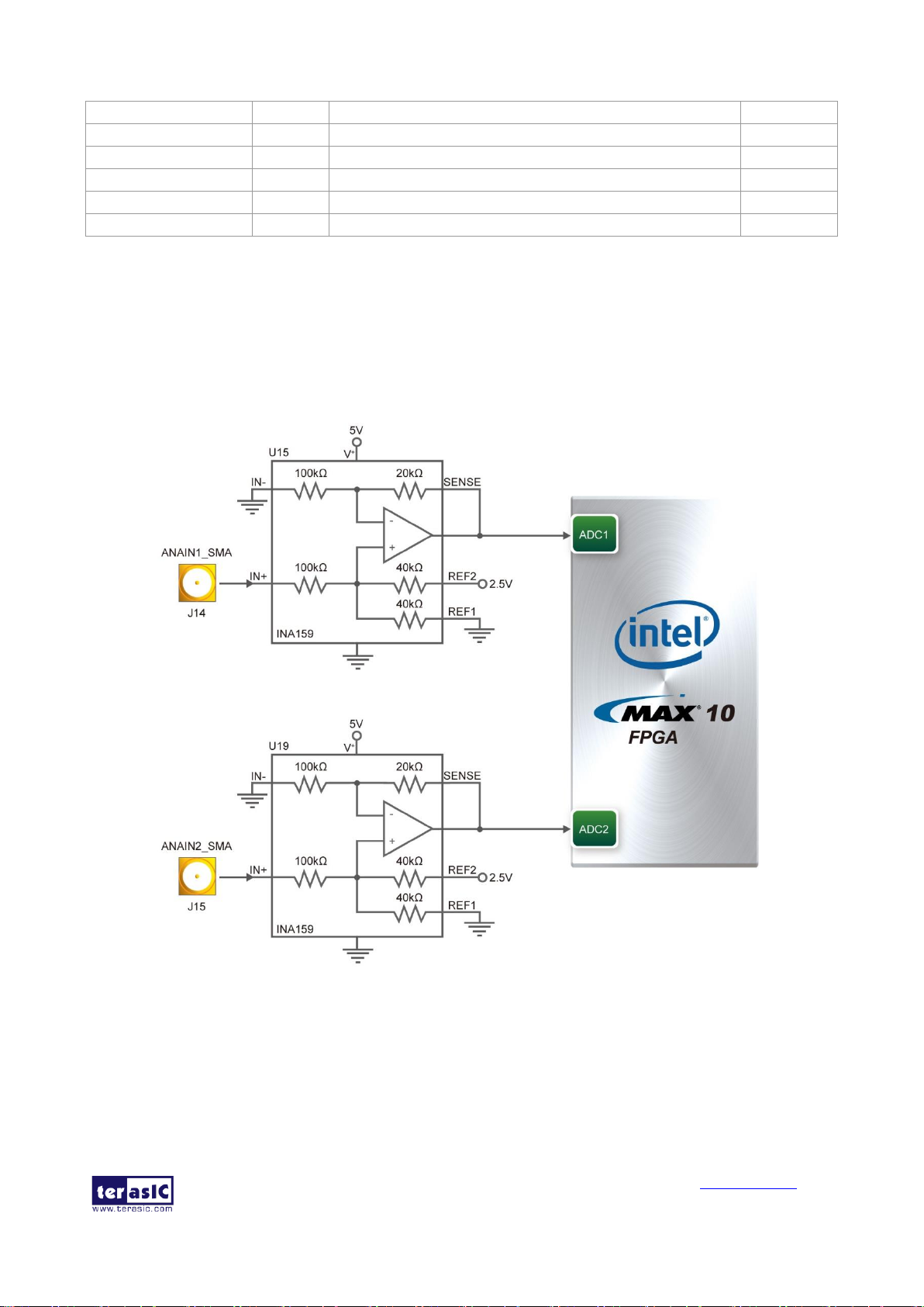
3.4.6 Two Analog Input SMA Connectors
The MAX 10 Plus implements two analog input SMA connectors. The analog inputs are amplified
and translated by Texas Instruments INA159 gain of 0.2 level translation difference amplifier, then
the amplifier’s outputs are fed to dedicated single-ended analog input pins for MAX 10 build-in
ADC1 and ADC2 respectively. With the amplifiers, the analog input of two SMAs support from
-6.25V to +6.25V range. Figure 3-19 shows the connection of SMA connectors to the FPGA.
Figure 3-19 Connection of SMA Connectors to the FPGA
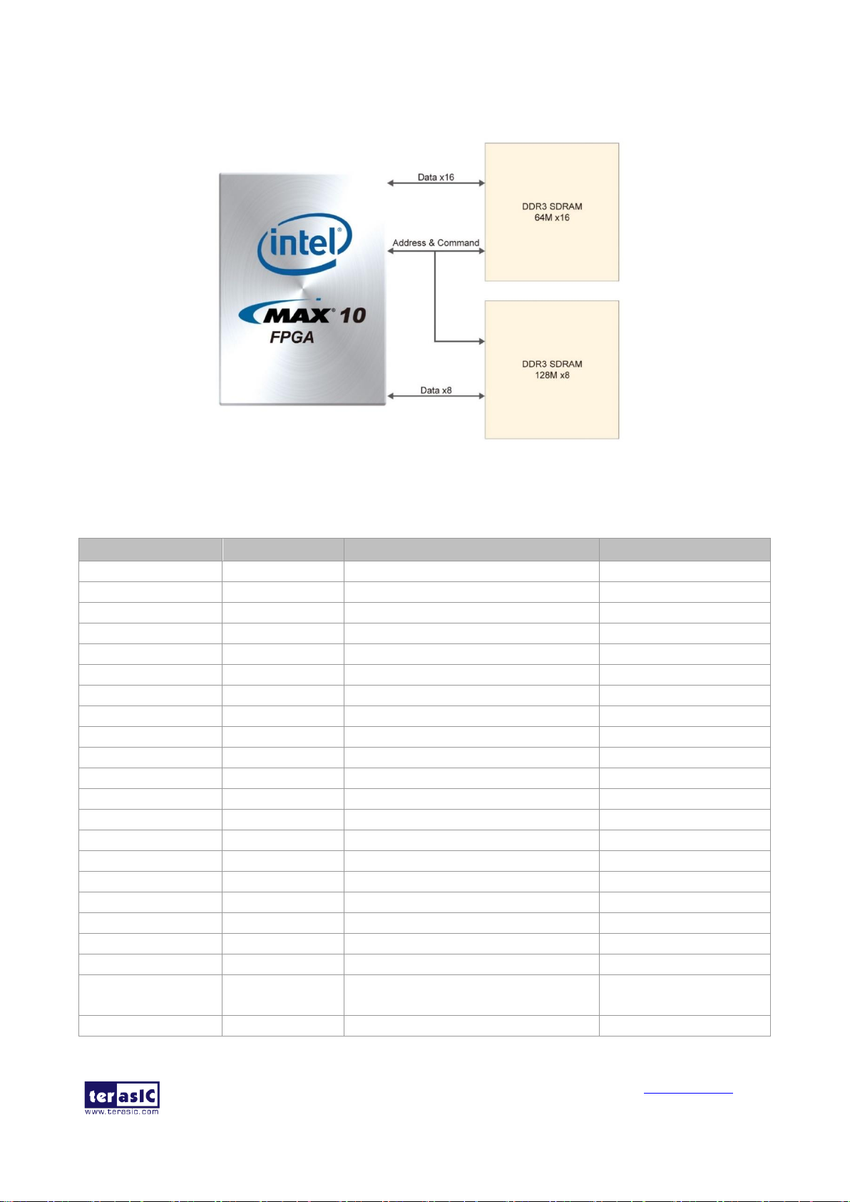
3.4.7 DDR3 Memory
The board supports 256MB of DDR3 SDRAM comprising of one 16bit (64Mx16) DDR3 device
and one 8bit (128Mx8) device. The DDR3 devices shipped with this board are running at 300MHz
with the soft IP of MAX 10 external memory interface solution. Figure 3-20 shows the connections
Page 24
MAX 10 Plus User
Manual
24
www.terasic.com
May 31, 2019
between the DDR3 and MAX 10 FPGA. Table 3-10 shows the DDR3 interface pin assignments.
Figure 3-20 Connections between the DDR3 and FPGA
Table 3-10 Pin Assignment of FPGA DDR3 Memory
Signal Name
FPGA Pin No.
Description
I/O Standard
DDR3_A[0]
PIN_U20
DDR3 Address[0]
SSTL-15 Class I
DDR3_A[1]
PIN_F19
DDR3 Address[1]
SSTL-15 Class I
DDR3_A[2]
PIN_V20
DDR3 Address[2]
SSTL-15 Class I
DDR3_A[3]
PIN_G20
DDR3 Address[3]
SSTL-15 Class I
DDR3_A[4]
PIN_F20
DDR3 Address[4]
SSTL-15 Class I
DDR3_A[5]
PIN_E20
DDR3 Address[5]
SSTL-15 Class I
DDR3_A[6]
PIN_E21
DDR3 Address[6]
SSTL-15 Class I
DDR3_A[7]
PIN_Y20
DDR3 Address[7]
SSTL-15 Class I
DDR3_A[8]
PIN_C22
DDR3 Address[8]
SSTL-15 Class I
DDR3_A[9]
PIN_D22
DDR3 Address[9]
SSTL-15 Class I
DDR3_A[10]
PIN_J14
DDR3 Address[10]
SSTL-15 Class I
DDR3_A[11]
PIN_E22
DDR3 Address[11]
SSTL-15 Class I
DDR3_A[12]
PIN_G22
DDR3 Address[12]
SSTL-15 Class I
DDR3_A[13]
PIN_D19
DDR3 Address[13]
SSTL-15 Class I
DDR3_A[14]
PIN_C20
DDR3 Address[14]
SSTL-15 Class I
DDR3_BA[0]
PIN_W22
DDR3 Bank Address[0]
SSTL-15 Class I
DDR3_BA[1]
PIN_Y21
DDR3 Bank Address[1]
SSTL-15 Class I
DDR3_BA[2]
PIN_Y22
DDR3 Bank Address[2]
SSTL-15 Class I
DDR3_CAS_n
PIN_U19
DDR3 Column Address Strobe
SSTL-15 Class I
DDR3_CKE
PIN_V18
Clock Enable pin for DDR3
SSTL-15 Class I
DDR3_CLK_n
PIN_E18
Clock n for DDR3
DIFFERENTIAL 1.5-V
SSTL Class I
DDR3_CLK_p
PIN_D18
Clock p for DDR3
Differential 1.5-V SSTL
Page 25

MAX 10 Plus User
Manual
25
www.terasic.com
May 31, 2019
Class I
DDR3_CS_n
PIN_W20
DDR3 Chip Select
SSTL-15 Class I
DDR3_DM[0]
PIN_J15
DDR3 Data Mask[0]
SSTL-15 Class I
DDR3_DM[1]
PIN_N19
DDR3 Data Mask[1]
SSTL-15 Class I
DDR3_DQ[0]
PIN_J18
DDR3 Data[0]
SSTL-15 Class I
DDR3_DQ[1]
PIN_H19
DDR3 Data[1]
SSTL-15 Class I
DDR3_DQ[2]
PIN_K20
DDR3 Data[2]
SSTL-15 Class I
DDR3_DQ[3]
PIN_H18
DDR3 Data[3]
SSTL-15 Class I
DDR3_DQ[4]
PIN_K18
DDR3 Data[4]
SSTL-15 Class I
DDR3_DQ[5]
PIN_H20
DDR3 Data[5]
SSTL-15 Class I
DDR3_DQ[6]
PIN_K19
DDR3 Data[6]
SSTL-15 Class I
DDR3_DQ[7]
PIN_J20
DDR3 Data[7]
SSTL-15 Class I
DDR3_DQ[8]
PIN_L18
DDR3 Data[8]
SSTL-15 Class I
DDR3_DQ[9]
PIN_M18
DDR3 Data[9]
SSTL-15 Class I
DDR3_DQ[10]
PIN_M14
DDR3 Data[10]
SSTL-15 Class I
DDR3_DQ[11]
PIN_N20
DDR3 Data[11]
SSTL-15 Class I
DDR3_DQ[12]
PIN_L20
DDR3 Data[12]
SSTL-15 Class I
DDR3_DQ[13]
PIN_M20
DDR3 Data[13]
SSTL-15 Class I
DDR3_DQ[14]
PIN_M15
DDR3 Data[14]
SSTL-15 Class I
DDR3_DQ[15]
PIN_L19
DDR3 Data[15]
SSTL-15 Class I
DDR3_DQ[16]
PIN_T19
DDR3 Data[15]
SSTL-15 Class I
DDR3_DQ[17]
PIN_R20
DDR3 Data[15]
SSTL-15 Class I
DDR3_DQ[18]
PIN_R15
DDR3 Data[15]
SSTL-15 Class I
DDR3_DQ[19]
PIN_P15
DDR3 Data[15]
SSTL-15 Class I
DDR3_DQ[20]
PIN_P19
DDR3 Data[15]
SSTL-15 Class I
DDR3_DQ[21]
PIN_P14
DDR3 Data[15]
SSTL-15 Class I
DDR3_DQ[22]
PIN_R14
DDR3 Data[15]
SSTL-15 Class I
DDR3_DQ[23]
PIN_P20
DDR3 Data[15]
SSTL-15 Class I
DDR3_DQS_n[0]
PIN_K15
DDR3 Data Strobe n[0]
Differential 1.5-V SSTL
Class I
DDR3_DQS_n[1]
PIN_L15
DDR3 Data Strobe n[1]
Differential 1.5-V SSTL
Class I
DDR3_DQS_p[0]
PIN_K14
DDR3 Data Strobe p[0]
Differential 1.5-V SSTL
Class I
DDR3_DQS_p[1]
PIN_L14
DDR3 Data Strobe p[1]
Differential 1.5-V SSTL
Class I
DDR3_ODT
PIN_V22
DDR3 On-die Termination
SSTL-15 Class I
DDR3_RAS_n
PIN_N18
DDR3 Row Address Strobe
SSTL-15 Class I
DDR3_RESET_n
PIN_B22
DDR3 Reset
SSTL-15 Class I
DDR3_WE_n
PIN_W19
DDR3 Write Enable
SSTL-15 Class I
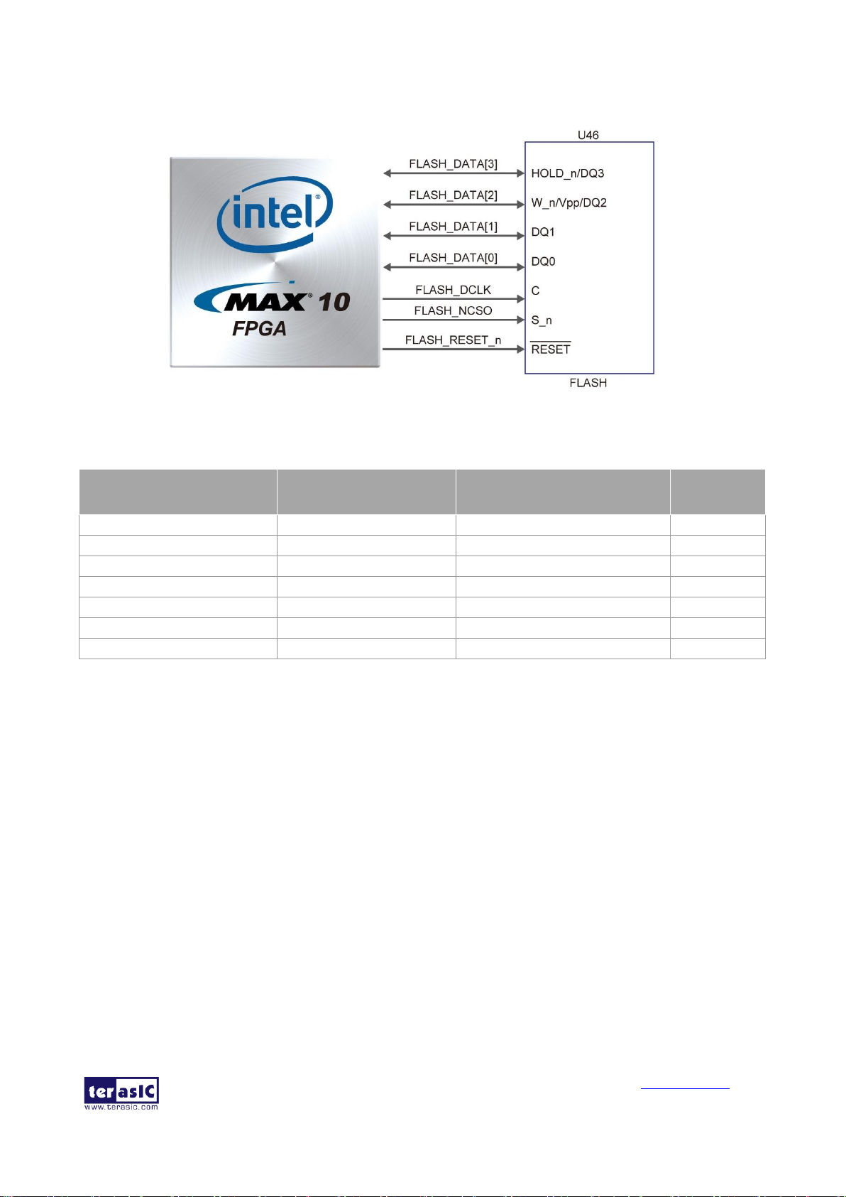
3.4.8 QSPI Flash
The MAX 10 Plus supports a 512M-bit serial NOR flash device for non-volatile storage, user data
and program. This device has a 4-bit data interface and uses 3.3V CMOS signaling standard.
Connections between MAX 10 FPGA and Flash are shown in Figure 3-21. Table 3-11 shows the
Page 26
MAX 10 Plus User
Manual
26
www.terasic.com
May 31, 2019
DDR3 interface pin assignments.
Figure 3-21 Connections between MAX 10 FPGA and QSPI Flash
Table 3-11 Pin Assignment of QSPI Flash
Signal Name
FPGA Pin No.
Description
I/O
Standard
FLASH_DATA[0]
PIN_AB18
FLASH Data[0]
3.3V
FLASH_DATA[1]
PIN_AA19
FLASH Data[1]
3.3V
FLASH_DATA[2]
PIN_AB19
FLASH Data[2]
3.3V
FLASH_DATA[3]
PIN_AA20
FLASH Data[3]
3.3V
FLASH_DCLK
PIN_AB17
FLASH Data Clock
3.3V
FLASH_NCSO
PIN_AB21
FLASH Chip Enable
3.3V
FLASH_RESET_n
PIN_AB20
FLASH Chip Reser
3.3V
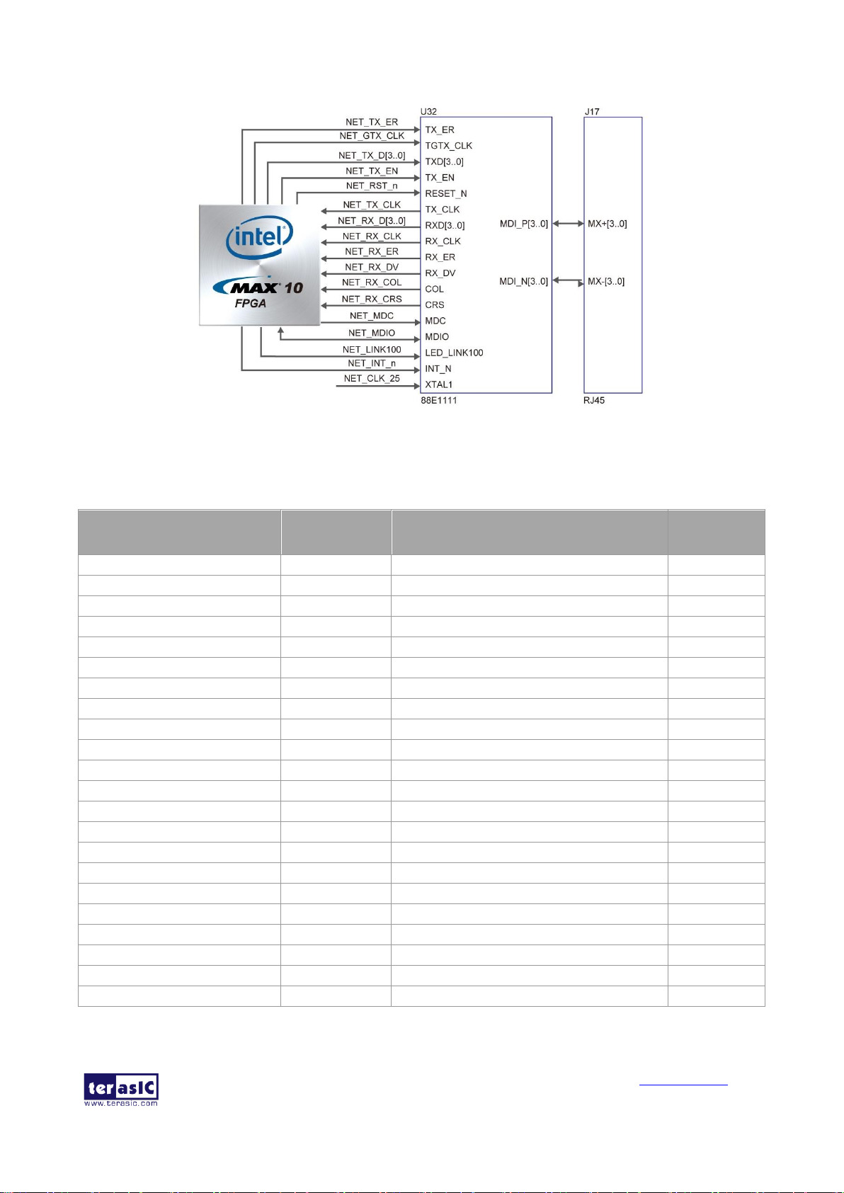
3.4.9 Ethernet
The board supports Gigabit Ethernet transfer by an external Marvell 88E1111 PHY chip. The
88E1111 chip with integrated 10/100/1000 Mbps Gigabit Ethernet transceiver support
GMII/MII/RGMII/TBI MAC interfaces. Figure 3-22 shows the connections between the MAX 10
FPGA, Ethernet PHY, and RJ-45 connector. The pin assignment associated to Gigabit Ethernet
interface is listed in Table 3-12.
Page 27
MAX 10 Plus User
Manual
27
www.terasic.com
May 31, 2019
Figure 3-22 Connections between the MAX 10 FPGA and Gigabit Ethernet
Table 3-12 Pin Assignment of Ethernet PHY
Signal Name
FPGA Pin No.
Description
I/O
Standard
NET_TX_EN
PIN_C10
GMII and MII transmit enable
2.5V
NET_TX_ER
PIN_C12
GMII and MII transmit error
2.5V
NET_TX_CLK
PIN_E11
MII transmit clock
3.3V
NET_TX_D[0]
PIN_A12
MII transmit data[0]
2.5V
NET_TX_D[1]
PIN_B12
MII transmit data[1]
2.5V
NET_TX_D[2]
PIN_A13
MII transmit data[2]
2.5V
NET_TX_D[3]
PIN_A14
MII transmit data[3]
2.5V
NET_RX_DV
PIN_A8
GMII and MII receive data valid
2.5V
NET_RX_ER
PIN_B8
GMII and MII receive data valid
2.5V
NET_RX_D[0]
PIN_A10
GMII and MII receive data[0]
2.5V
NET_RX_D[1]
PIN_B10
GMII and MII receive data[1]
2.5V
NET_RX_D[2]
PIN_A11
GMII and MII receive data[2]
2.5V
NET_RX_D[3]
PIN_B11
GMII and MII receive data[3]
2.5V
NET_RX_CLK
PIN_J10
GMII and MII receive clock
3.3V
NET_RST_n
PIN_C14
Hardware Reset Signal
2.5V
NET_MDIO
PIN_E12
Management Data
2.5V
NET_MDC
PIN_D12
Management Data Clock Reference
2.5V
NET_RX_COL
PIN_C9
GMII and MII collision
2.5V
NET_RX_CRS
PIN_A9
GMII and MII carrier sense
2.5V
NET_GTX_CLK
PIN_C11
GMII Transmit Clock
2.5
NET_LINK100
PIN_A7
Parallel LED output of 100BASE-TX link
2.5V
NET_INT_n
PIN_C13
Interrupt open drain output
2.5V
Page 28

MAX 10 Plus User
Manual
28
www.terasic.com
May 31, 2019
3.4.10 HDMI RX
The development board provides High Performance HDMI Receiver via the Analog Devices
ADV7611 which incorporates HDMI v1.4a features, including 3D video support, and 165MHz
supports all video formats up to 1080p and UXGA. The ADV7611 is controlled via a serial I2C bus
interface, which is connected to pins on the MAX 10 FPGA. A schematic diagram of the HDMI RX
circuitry is shown in Figure 3-23. Detailed information on using the ADV7611 HDMI RX is
available on the manufacturer’s website, or under the Datasheets\HDMI folder on the Kit System
CD.
Table 3-13 lists the HDMI Interface pin assignments and signal names relative to the MAX 10
device.
Figure 3-23 Connection between the MAX 10 FPGA and HDMI Receiver
Table 3-13 Pin Assignment of HDMI RX
Signal Name
FPGA Pin No.
Description
I/O Standard
HDMI_RX_D0
PIN_AA9
Video Pixel Output Port
3.3V
HDMI_RX_D1
PIN_AB9
Video Pixel Output Port
3.3V
HDMI_RX_D2
PIN_Y10
Video Pixel Output Port
3.3V
HDMI_RX_D3
PIN_AA10
Video Pixel Output Port
3.3V
HDMI_RX_D4
PIN_AB10
Video Pixel Output Port
3.3V
HDMI_RX_D5
PIN_Y11
Video Pixel Output Port
3.3V
HDMI_RX_D6
PIN_AA11
Video Pixel Output Port
3.3V
HDMI_RX_D7
PIN_AB11
Video Pixel Output Port
3.3V
HDMI_RX_D8
PIN_Y14
Video Pixel Output Port
3.3V
HDMI_RX_D9
PIN_AB15
Video Pixel Output Port
3.3V
HDMI_RX_D10
PIN_AA15
Video Pixel Output Port
3.3V
HDMI_RX_D11
PIN_W14
Video Pixel Output Port
3.3V
HDMI_RX_D12
PIN_V14
Video Pixel Output Port
3.3V
HDMI_RX_D13
PIN_V15
Video Pixel Output Port
3.3V
HDMI_RX_D14
PIN_U15
Video Pixel Output Port
3.3V
Page 29

MAX 10 Plus User
Manual
29
www.terasic.com
May 31, 2019
HDMI_RX_D15
PIN_AB14
Video Pixel Output Port
3.3V
HDMI_RX_D16
PIN_AA14
Video Pixel Output Port
3.3V
HDMI_RX_D17
PIN_AB13
Video Pixel Output Port
3.3V
HDMI_RX_D18
PIN_Y13
Video Pixel Output Port
3.3V
HDMI_RX_D19
PIN_AB12
Video Pixel Output Port
3.3V
HDMI_RX_D20
PIN_AA12
Video Pixel Output Port
3.3V
HDMI_RX_D21
PIN_W13
Video Pixel Output Port
3.3V
HDMI_RX_D22
PIN_W12
Video Pixel Output Port
3.3V
HDMI_RX_D23
PIN_V13
Video Pixel Output Port
3.3V
HDMI_RX_CLK
PIN_P11
Line-Locked Output Clock
3.3V
HDMI_RX_DE
PIN_W10
Data Enable Signal for Digital Video.
3.3V
HDMI_RX_HS
PIN_V12
Horizontal Synchronization
3.3V
HDMI_RX_VS
PIN_W11
Vertical Synchronization
3.3V
HDMI_RX_INT1
PIN_P12
Interrupt Signal
3.3V
HDMI_I2C_SCL
PIN_R13
I2C Clock
3.3V
HDMI_I2C_SDA
PIN_P13
I2C Data
3.3V
HDMI_MCLK
PIN_R12
Audio Master Output Clock
3.3V
HDMI_LRCLK
PIN_V11
Audio Left/Right Clock
3.3V
HDMI_SCLK
PIN_W8
Audio Serial Output Clock
3.3V
HDMI_AP
PIN_W9
Audio Output Pin
3.3V
HDMI_RX_RESET_n
PIN_AA13
System Reset Input
3.3V
3.4.11 2x10 ADC Header
The board has a 2x10 ADC header with sixteen analog inputs connected to FPGA ADC1 and ADC2
respectively. The 1x3 header J12 is used to select pin 18 of 2x10 header J7 or potentiometer input to
be connected to the channel 8 of FPGA ADC2. Short pin 1 and pin 2 of J12 to select potentiometer,
short pin 3 and pin 4 to select pin 18 of 2x10 header J7. The 1x3 header J13 is used to select pin 16
of 2x10 header J7 or on-board microphone to be connected to the channel 7 of FPGA ADC2. Short
pin 1 and pin 2 of J13 to select on-board microphone, short pin 3 and pin 4 to select pin 16 of 2x10
header J7. Figure 3-24 shows the connection of 2x10 ADC header and MAX 10 FPGA.
Page 30

MAX 10 Plus User
Manual
30
www.terasic.com
May 31, 2019
Figure 3-24 Connections between 2x10 ADC Header, Potentiometer, On-board Microphone
and MAX 10 FPGA
3.4.12 Potentiometer
Short pin 1 and pin 2 of J12 will select potentiometer for providing adjustable voltage to the
channel 8 of FPGA ADC2.
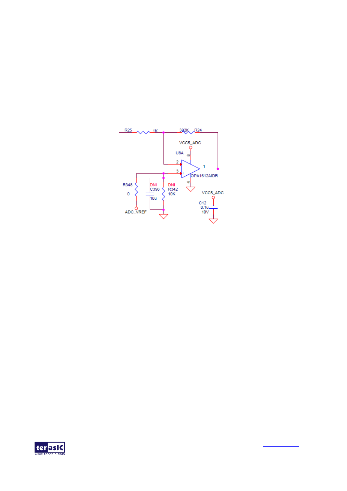
3.4.13 On-board Microphone
The board provides an on-board microphone for audio applications. Short pin 1 and pin 2 of J13 to
select on-board microphone to be connected to the channel 7 of FPGA ADC2. The output audio
signal from on-board microphone will be pre-amplified by audio operational amplifier OPA1612,
then fed into the FPGA ADC. Figure 3-24 shows the connection of on-board microphone and MAX
10 FPGA.
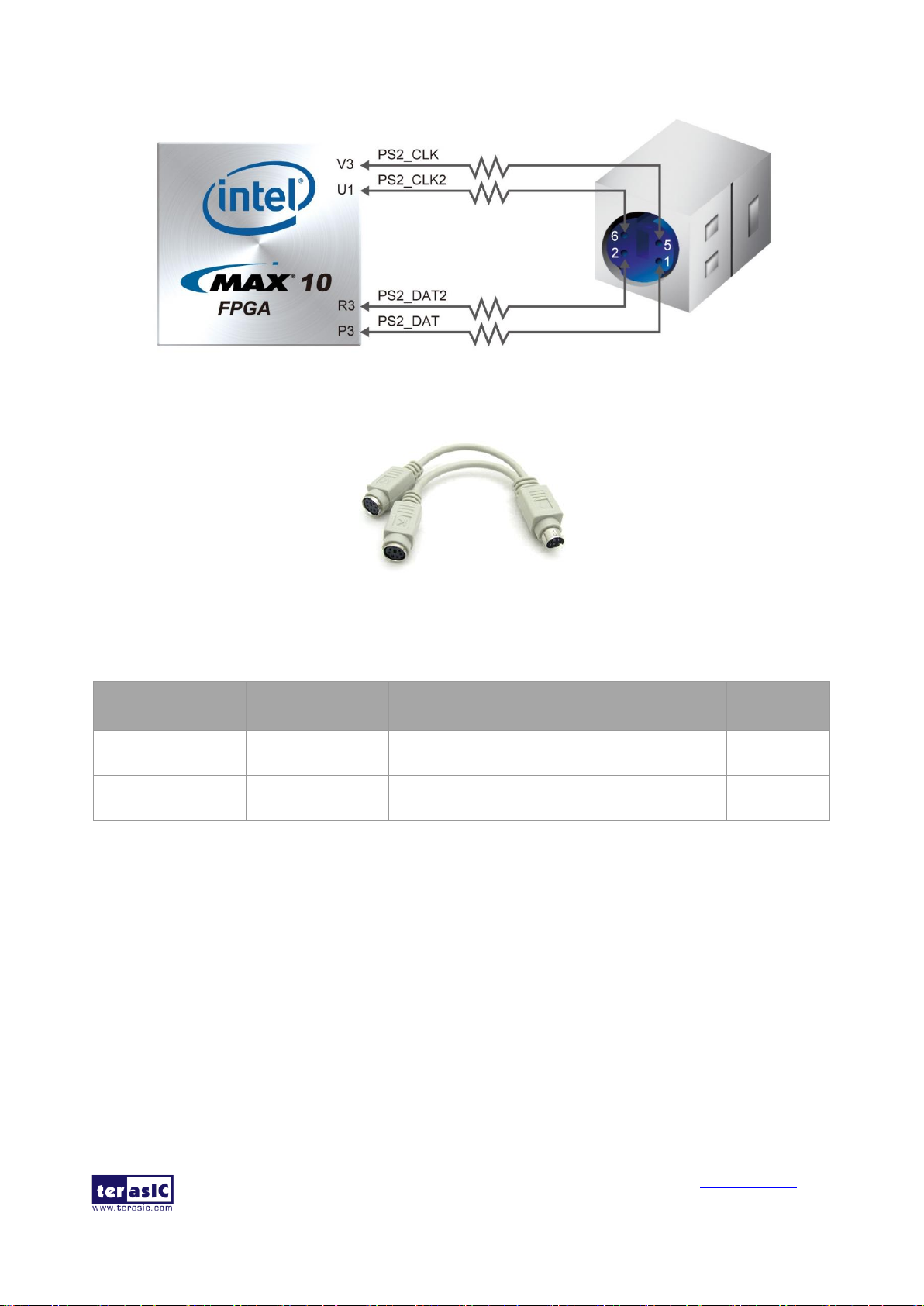
3.4.14 PS/2 Serial Port
The MAX 10 Plus comes with a standard PS/2 interface and a connector for a PS/2 keyboard or
mouse. Figure 3-25 shows the connection of PS/2 circuit to the FPGA. Users can use the PS/2
keyboard and mouse on the MAX 10 Plus simultaneously by a PS/2 Y-Cable, as shown in Figure
3-26. Instructions on how to use PS/2 mouse and/or keyboard can be found on various educational
websites. The pin assignment associated to this interface is shown in Table 3-14.
Note: If users connect only one PS/2 equipment, the PS/2 signals connected to the FPGA I/O
should be “PS2_CLK” and “PS2_DAT”.
Page 31
MAX 10 Plus User
Manual
31
www.terasic.com
May 31, 2019
Figure 3-25 Connections between the MAX 10 FPGA and PS/2
Figure 3-26 Y-Cable for Using Keyboard and Mouse Simultaneously
Table 3-14 Pin Assignment of PS/2
Signal Name
FPGA Pin No.
Description
I/O
Standard
PS2_CLK
PIN_V3
PS/2 Clock
3.3V
PS2_DAT
PIN_P3
PS/2 Data
3.3V
PS2_CLK2
PIN_U1
PS/2 Clock (reserved for second PS/2 device)
3.3V
PS2_DAT2
PIN_R3
PS/2 Data (reserved for second PS/2 device)
3.3V
3.4.15 Digital-to-Analog Converter (DAC)
The board provides a Texas Instruments DAC8551 16-bit digital-to-analog converter (DAC). It is a
small, low power, voltage output DAC. The DAC8551 used a versatile 3-wire serial interface that
operates at clock rates to 30MHz and is compatible with standard SPI, QSPI, Microwire and DSP
interfaces. The analog voltage output of DAC8551 is connected to a SMA connector. Figure 3-27
shows the connection between DAC and MAX 10 FPGA. The pin assignment associated to this
DAC is shown in Table 3-15.
Page 32

MAX 10 Plus User
Manual
32
www.terasic.com
May 31, 2019
Figure 3-27 Connection between DAC and MAX 10 FPGA
Table 3-15 Pin Assignment of DAC
Signal Name
FPGA Pin No.
Description
I/O Standard
DAC_SYNC_n
PIN_B2
Frame Sync Signal for Input Data
3.3V
DAC_SCLK
PIN_B1
Serial Clock Input
3.3V
DAC_DATA
PIN_A2
Serial Data Input
3.3V
3.4.16 UART to USB
The board has one UART interface connected for communication with the MAX 10 FPGA. This
interface doesn’t support HW flow control signals. The physical interface is implemented by
UART-USB onboard bridge from a FT232R chip to the host with an USB Mini-B connector. More
information about the chip is available on the manufacturer’s website, or in the directory
\Datasheets\UART TO USB of MAX 10 Plus system CD. Figure 3-28 shows the connections
between the MAX 10 FPGA, FT232R chip, and the USB Mini-B connector. Table 3-16 lists the pin
assignment of UART interface connected to the MAX 10 FPGA.
Figure 3-28 Connections between the HPS and FT232R Chip
Page 33

MAX 10 Plus User
Manual
33
www.terasic.com
May 31, 2019
Table 3-16 Pin Assignment of UART Interface
Signal Name
FPGA Pin No.
Description
I/O Standard
UART_RX
PIN_E16
FPGA UART Receiver
2.5V
UART_TX
PIN_E15
FPGA UART Transmitter
2.5V
UART_RESET_n
PIN_D15
Reset Signal for UART Device
2.5V
3.4.17 Ambient Light Sensor
The MAX 10 Plus has a Light-to-Digital Ambient Light Sensor (APDS-9301) that converts light
intensity to digital signal output capable of I2C interface. with I2C digital interface and
programmable-event interrupt output. The digital output of APDS-9301 will be input to the MAX
10 FPGA where illuminance I lux is derived using an empirical formula to approximate the
human-eye response. Figure 3-29 shows the connection of APDS-9301 to the MAX 10 FPGA.
Table 3-17 lists the Ambient Light Sensor pin assignments.
Figure 3-29 The Connections between the MAX 10 FPGA and Ambient Light Sensor
Table 3-17 Pin Assignment of Ambient Light Sensor
Signal Name
FPGA Pin No.
Description
I/O Standard
LSENSOR_SCL
PIN_M1
I2C Serial Clock
3.3V
LSENSOR_SDA
PIN_T3
I2C Serial Data
3.3V
LSENSOR_INT
PIN_M2
Interrupt signal from Sensor
3.3V
3.4.18 Humidity and Temperature Sensor
The MAX 10 Plus has a humidity and temperature sensor (HDC1000) that provides excellent
measurement accuracy at very low power. The HDC1000 sensor is placed at board edge and away
from the heat source of MAX 10 Plus so that user can make ambient temperature measurement
without heat interference from the heat source of MAX 10 Plus. Figure 3-30 shows the connection
of humidity and temperature sensor to MAX 10 FPGA. Table 3-18 lists the humidity and
temperature sensor pin assignments.
Page 34

MAX 10 Plus User
Manual
34
www.terasic.com
May 31, 2019
Figure 3-30 The Connections between the MAX 10 FPGA and Humidity and Temperature
Sensor
Table 3-18 Pin Assignment of Humidity and Temperature Sensor
Signal Name
FPGA Pin No.
Description
I/O Standard
RH_TEMP_I2C_SCL
PIN_Y18
I2C Clock for HDC1000 Sensor
3.3V
RH_TEMP_I2C_SDA
PIN_W18
I2C Data for HDC1000 Sensor
3.3V
RH_TEMP_DRDY_n
PIN_Y19
Data ready input from HDC1000 Sensor
3.3V
3.4.19 Accelerometer Sensor
The board comes with a digital accelerometer sensor module (ADXL345), commonly known as
G-sensor. This G-sensor is a small, thin, ultralow power assumption 3-axis accelerometer with
high-resolution measurement. Digitalized output is formatted as 16-bit in two’s complement and
can be accessed through I2C interface. The I2C address of accelerometer is 0xA6/0xA7. More
information about this chip can be found in its datasheet, which is available on manufacturer’s
website or in the directory \Datasheet folder of MAX 10 Plus system CD. Figure 3-31 shows the
connections between the MAX 10 FPGA and accelerometer. Table 3-19 lists the pin assignment of
accelerometer to the MAX 10 FPGA.
Figure 3-31 The Connections between the MAX 10 FPGA and Accelerometer Sensor
Page 35

MAX 10 Plus User
Manual
35
www.terasic.com
May 31, 2019
Table 3-19 Pin Assignment of Accelerometer Sensor
Signal Name
FPGA Pin No.
Description
I/O
Standard
GSENSOR_SDI
PIN_C15
I2C serial data/SPI serial data input/3-wire
interface serial dta output
2.5V
GSENSOR_SDO
PIN_B16
SPI serial data output/I2C less significant bit
of the device address
2.5V
GSENSOR_CS_n
PIN_C16
SPI enable, I2C/SPI mode selection: 1: SPI
idle mode/I2C communication enabled, 0:
SPI communication mode/I2C disabled
2.5V
GSENSOR_SCLK
PIN_A15
I2C serial clock/SPI serial port clock
2.5V
GSENSOR_INT1
PIN_B15
Interrupt pin 1
2.5V
GSENSOR_INT2
PIN_D17
Interrupt pin 2
2.5V
3.4.20 Micro SD Card Socket
The board supports Micro SD card interface with x4 data lines. It serves not only an external
storage for the HPS, but also an alternative boot option for MAX 10 Plus. Figure 3-32 shows
signals connected between the HPS and Micro SD card socket.
Table 3-20 lists the pin assignment of Micro SD card socket to the MAX 10 FPGA.
Figure 3-32 Connections between the MAX 10 FPGA and SD Card Socket
Table 3-20 Pin Assignment of Micro SD Card Socket
Signal Name
FPGA Pin No.
Description
I/O Standard
SD_CLK
PIN_A16
SD Clock
2.5V
SD_CMD
PIN_C18
SD Command Line
2.5V
SD_DATA[0]
PIN_A17
SD Data[0]
2.5V
SD_DATA[1]
PIN_A18
SD Data[1]
2.5V
SD_DATA[2]
PIN_B17
SD Data[2]
2.5V
SD_DATA[3]
PIN_C17
SD Data[3]
2.5V
3.4.21 Power Distribution System
The MAX 10 Plus is powered by Linear Technology’s power solution which provides
Page 36

MAX 10 Plus User
Manual
36
www.terasic.com
May 31, 2019
high-efficiency power management for FPGAs and SoCs. Figure 3-33 shows the power tree of
MAX 10 Plus. Note that the LCD interface are reserved.
Figure 3-33 Power Tree of MAX 10 Plus
Page 37

MAX 10 Plus User
Manual
37
www.terasic.com
May 31, 2019
Chapter 4
The MAX 10 Plus System Builder
This chapter introduces the MAX 10 Plus System Builder to help users get started in creating their
own projects in literally minutes. It also describes the design flow and includes an example for users
to get familiar with the tool.
4.1 Introduction
The MAX 10 Plus System Builder is a Windows-based utility. It is created to help users build a top
project for MAX 10 Plus within minutes. The generated Quartus II project files include:
• Quartus II project file (.qpf)
• Quartus II setting file (.qsf)
• Top-level design file (.v)
• Synopsis design constraints file (.sdc)
• Pin assignment document (.htm)
The above files generated by the MAX 10 Plus System Builder can also prevent situations that are
prone to compilation error when users manually edit the top-level design file or place pin
assignment. The common mistakes that users encounter are:
• Board is damaged due to incorrect bank voltage setting or pin assignment.
• Board is malfunctioned because of wrong device chosen, declaration of pin location, or the
direction is incorrect/forgotten.
• Performance degradation due to improper pin assignment.
4.2 General Design Flow
The design flow of building a Quartus II project for MAX 10 Plus using the MAX 10 Plus System
Builder is illustrated in Figure 4-1. It gives users an overview about the steps, starting from
launching the System Builder to configuring the FPGA. The left-hand side of the chart can be done
within minutes. After users enter the design requirements, the MAX 10 Plus System Builder will
generate Quartus II project files, Quartus II setting file, top-level design file, Synopsis design
constraint file, and the pin assignment document.
The top-level design file contains a top-level Verilog HDL wrapper for users to add their own
design/logic. The Quartus II setting file contains information such as FPGA device type, top-level
pin assignment, and the I/O standard for each user-defined I/O pin. These files can be modified
according to the project requirements. After the compilation is successful, users can download
the .sof file to the development board via JTAG interface using the Quartus II programmer.
Page 38

MAX 10 Plus User
Manual
38
www.terasic.com
May 31, 2019
Figure 4-1 Design Flow of Building a Project from the beginning to the end
4.3 Using MAX 10 Plus System Builder
This section provides the procedures in details on how to use the MAX 10 Plus System Builder.
◼ Install and Launch the MAX 10 Plus System Builder
The MAX 10 Plus System Builder is located in the directory Tools\SystemBuilder of the MAX 10
Plus System CD. Users can copy the entire folder to a host PC without installing the utility. After
the execution of the MAX 10 Plus SystemBuilder.exe on the host PC, a window will pop up, as
shown in Figure 4-2.
Page 39

MAX 10 Plus User
Manual
39
www.terasic.com
May 31, 2019
Figure 4-2 The GUI of MAX 10 Plus System Builder
◼ Enter Project Name
The project name entered in the circled area, as shown in Figure 4-3, will be assigned automatically
as the name of the top-level design entity.
Page 40

MAX 10 Plus User
Manual
40
www.terasic.com
May 31, 2019
Figure 4-3 Enter the Project Name
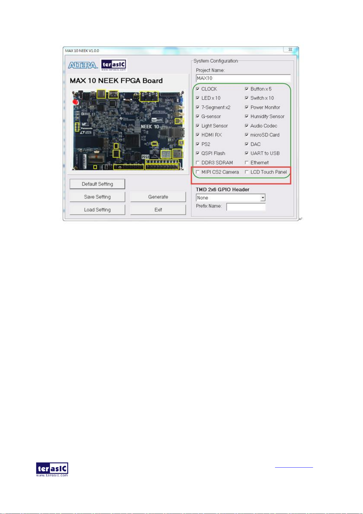
◼ System Configuration
Users are given the flexibility in the System Configuration to include one or more onboard
peripherals in the project, as shown in Figure 4-4. If a component is enabled, the MAX 10 Plus
System Builder will automatically generate its associated pin assignment, including the pin name,
pin location, pin direction, and I/O standard.
Note: The MIPI CS2 Camera and LCD Touch Panel interfaces are reserved, users can choose to buy
MAX 10 NEEK instead if needed these two interfaces.
Page 41
MAX 10 Plus User
Manual
41
www.terasic.com
May 31, 2019
Figure 4-4 List of onboard Peripherals in System Configuration
◼ Project Settings
The MAX 10 Plus System Builder also provides the option to load a setting or save the current
board configuration in .cfg file, as shown in Figure 4-5.
Page 42

MAX 10 Plus User
Manual
42
www.terasic.com
May 31, 2019
Figure 4-5 Manage Project Settings
◼ Project Generation
When users press the Generate button, as shown in Figure 4-6, the MAX 10 Plus System Builder
will generate the corresponding Quartus II files and documents, as listed in Table 4-1.
Page 43

MAX 10 Plus User
Manual
43
www.terasic.com
May 31, 2019
Figure 4-6 Generate Quartus Project
Table 4-1 Files Generated by the MAX 10 Plus System Builder
No.
Filename
Description
1
<Project name>.v
Top-level Verilog HDL file for Quartus II
2
<Project name>.qpf
Quartus II project file
3
<Project name>.qsf
Quartus II setting file
4
<Project name>.sdc
Synopsis design constraints file for Quartus II
5
<Project name>.htm
Pin assignment document
Users can add custom logic into the project and compile the project in Quartus II to generate the
SRAM Object File (.sof).
Page 44

MAX 10 Plus User
Manual
44
www.terasic.com
May 31, 2019
Chapter 5
RTL Example Codes
This chapter provides examples of advanced designs implemented by RTL on the MAX 10 Plus
board. These reference designs cover the features of peripherals connected to the FPGA, such as
PS/2 mouse, ADC/DAC application. All the associated files can be found in the directory
\Demonstrations of System CD. Note: The output files generated after compilation in Quartus II
e.g. .sof and .pof files, are saved in the folder "output_files" under the directory of demo project.
5.1 PS/2 Mouse Demonstration
We offer this simple PS/2 controller coded in Verilog HDL to demonstrate bidirectional
communication between PS/2 controller and the device, the PS/2 mouse. You can treat it as a
how-to basis and develop your own controller that could accomplish more sophisticated instructions,
like setting the sampling rate or resolution, which need to transfer two data bytes.
More information about the PS/2 protocol can be found on various websites.
◼ Introduction
PS/2 protocol uses two wires for bi-directional communication. One is the clock line and the other
one is the data line. The PS/2 controller always has total control over the transmission line, but it is
the PS/2 device which generates the clock signal during data transmission.
◼ Data Transmission from Device to the Controller
After the PS/2 mouse receives an enabling signal at stream mode, it will start sending out
displacement data, which consists of 33bits. The frame data is cut into three sections and each of
them contains a start bit (always zero), eight data bits (with LSB first), one parity check bit (odd
check), and one stop bit (always one).
The PS/2 controller samples the data line at the falling edge of the PS/2 clock signal. This is
implemented by a shift register, which consists of 33bits, but please be cautious with the clock
domain crossing problem.
◼ Data Transmission from the Controller to Device
When the PS/2 controller wants to transmit data to device, it first pulls the clock line low for more
than one clock cycle to inhibit the current transmission process or to indicate the start of a new
transmission process, which is usually called as inhibit state. It then pulls low the data line before
releasing the clock line. This is called the request state. The rising edge on the clock line formed by
the release action can also be used to indicate the sample time point as for a start bit. The device
will detect this succession and generates a clock sequence in less than 10ms time. The transmit data
consists of 12bits, one start bit (as explained before), eight data bits, one parity check bit (odd
check), one stop bit (always one), and one acknowledge bit (always zero).
Page 45

MAX 10 Plus User
Manual
45
www.terasic.com
May 31, 2019
After sending out the parity check bit, the controller should release the data line, and the device will
detect any state change on the data line in the next clock cycle. If there’s no change on the data line
for one clock cycle, the device will pull low the data line again as an acknowledgement which
means that the data is correctly received.
After the power-on cycle of the PS/2 mouse, it enters into stream mode automatically and disable
data transmit unless an enabling instruction is received. Figure 5-1 shows the waveform while
communication happening on two lines.
Figure 5-1 Waveform of Clock and Data Signals during Data Transmission
◼ Design Tools
• Quartus II v15.0 64-bit
◼ Demonstration Source Code
• Project directory: ps2_mouse
• Bitstream used: ps2_mouse.sof
◼ Demonstration Batch File
• Demo batch file folder: Demonstrations\ps2_mouse\demo_batch
• Batch file: ps2_mouse.bat
• FPGA configuration file: ps2_mouse.sof
Page 46

MAX 10 Plus User
Manual
46
www.terasic.com
May 31, 2019
◼ Demonstration Setup
• Please make sure Quartus II and USB-Blaster II driver are installed on the host PC.
• Connect the USB cable from the USB-Blaster II port (J8) on the MAX 10 Plus board to the host
PC and power on the MAX 10 Plus board.
• Execute the demo batch file “ps2_mouse.bat” under the folder
Demonstrations\ps2_mouse\demo_batch\.
• Plug in the PS/2 mouse.
• Press KEY0 to enable data transfer.
• Press KEY1 to clear the display data cache.
• The 7-segment display shows X displacement when SW0 is low, and Y displacement when SW0
is high. The display should change when the PS/2 mouse moves.
• The LEDR [2:0] will blink according to Table 5-1 when the left-button, right-button, and/or
middle-button is pressed.
Table 5-1 Description of 7-segment Display and LED Indicators
Indicator Name
Description
LEDR0
Left button press indicator
LEDR1
Right button press indicator
LEDR2
Middle button press indicator
HEX0
Low byte of X/Y displacement
HEX1
High byte of X/Y displacement
5.2 ADC Potentiometer
Nowadays voltage and current monitors play a significant role in high-reliability system. Most of
applications can be implemented by an Analog-to-Digital Converter (ADC). MAX 10 Plus board
provides a potentiometer demonstration using the ADC in MAX10. This ADC solution consists of
hard IP blocks in MAX 10 device and soft logic through Intel Modular ADC IP core. Figure 5-2
shows the block diagram of ADC hard IP block in MAX10 device.
Figure 5-2 Block Diagram of ADC Hard IP Block
This demo uses 2nd ADC of MAX10 on channel 8. The ADC settings are shown in Figure 5-3.
Page 47

MAX 10 Plus User
Manual
47
www.terasic.com
May 31, 2019
Figure 5-3 Settings of ADC Hard IP
The MAX 10 Plus board has a Variable Resistor (VR) onboard, which acts as a potentiometer in this
demonstration. Figure 5-4 shows the block diagram of Power Monitor demonstration. The ADC
reference clock running at 10MHz is generated by PLL. It feeds into the ADC Hard IP in MAX10
device. The analog voltage input comes from the VR controls the voltage level. The control logic
within the ADC Hard IP reads the digitized voltage data. It then converts the data and displays the
level value on two 7-segments. Since none of the dot points of two 7-segments is connected to the
MAX 10, so HEX1 and HEX0 shows the decimal point and the first digit after the decimal point
respectively.
Figure 5-4 Block Diagram of ADC Potentiometer
◼ Design Tools
• Quartus II v15.0 64-bit
Page 48

MAX 10 Plus User
Manual
48
www.terasic.com
May 31, 2019
◼ Demonstration Source Code
• Project directory: Demonstrations\adc_potentionmeter
• Bitstream used: adc_potentionmeter.sof
◼ Demonstration Batch File
• Demo batch file folder: Demonstrations\adc_potentionmeter \demo_batch
• Batch file: test.bat
• FPGA configuration file: adc_potentionmeter.sof
◼ Demonstration Setup
• Please make sure Quartus II and USB-Blaster II driver are installed on the host PC.
• Connect the USB cable from the USB-Blaster II port (J8) on the MAX 10 Plus board to the host
PC.
• Power on the MAX 10 Plus board.
• Execute the demo batch file “test.bat” under the folder Demonstrations\ adc_potentionmeter
\demo_batch.
• Rotate the VR resistor POT1 with a screwdriver. HEX1 and HEX0 will display the voltage
value.
5.3 DAC Demonstration
This demonstration uses the 16-bit Digital to analog converter (DAC) built-in the MAX 10 device
to generate square wave in 8 difference frequencies. The signal coming out of the SMA connector
on MAX 10 Plus board is transmitted to the oscilloscope. The oscilloscope will display the square
wave in different frequencies by switching SW [2:0] on the MAX 10 Plus board.
◼ Function Block Diagram
Figure 5-5 is the function block diagram of this demonstration. The source data in parallel is
converted to serial data by the DAC16 module. The DAC chip (DAC8551) then converts the serial
data from digital to analog. The analog signal coming out of the DAC SMA connector is connected
to the oscilloscope and shown in square wave. Users can switch the SW0~2 to change the frequency
of the square wave.
Page 49

MAX 10 Plus User
Manual
49
www.terasic.com
May 31, 2019
Figure 5-5 Block Diagram of the DAC Demo
◼ Design Tools
• Quartus II v15.0 64-bit
◼ Demonstration Source Code
• Project directory: Demonstrations\ dac_sma
• Bitstream used: dac_sma.sof
◼ Demonstration Batch File
• Demo batch file folder: Demonstrations\ dac_sma\demo_batch
• Batch file: test.bat
• FPGA configuration file: dac_sma.sof
◼ Demonstration Setup
• Please make sure Quartus II and USB-Blaster II driver are installed on the host PC.
• Connect the USB cable from the USB-Blaster II port (J8) to the host PC.
• Plug in the 5V adapter to the MAX 10 Plus board and power it up.
• Execute the demo batch file “test.bat” from the directory \ dac_sma\demo_batch.
• Connect the probe of the oscilloscope to the DAC SMA OUT of the MAX 10 Plus board and
adjust the display until the square wave is visible, as Figure 5-6 and Figure 5-7.
• Switch SW [2:0] from 000 to 111 and the frequency of the square will be changing. The
square-wave frequency is twice higher. When SW [2:0]=000, the square wave frequency is
about 2.6KHz; When SW[2:0]=111, the frequency is about 112KHz.
Page 50

MAX 10 Plus User
Manual
50
www.terasic.com
May 31, 2019
Figure 5-6 Use the Oscilloscope to Observe the Square Wave
Figure 5-7 Probe DAC SMA OUT from the Oscilloscope
Page 51
MAX 10 Plus User
Manual
51
www.terasic.com
May 31, 2019
5.4 ADC/MIC/LED Demonstration
There is a high-sensitive microphone on the MAX 10 Plus board to receive the surrounding sound.
After the sound is collected and amplified approximately 392 times, as shown in Figure 5-8, it is
feed into the ADC of MAX 10 device. The digitized waveform will be displayed on the LED.
Meanwhile the signal will be sent to the Line-out via audio codec and DAC SMA OUT connector.
Both of which can be connected to an external speaker. The data will also be processed based on the
volume to be displayed on the 10 LEDs onboard.
Figure 5-8 Onboard Microphone Amplifier with Gain (R24/R25) = 392
◼ Function Block Diagram
Figure 5-9 is the function block diagram of this demonstration. The built-in MIC is amplified
approximately 392 times via two operational amplifiers. The signal is then feed into the ADC of
MAX 10 device for conversion. This demonstration uses the timing from the audio codec
((TLV320AIC3254) via I2S protocol to sync the entire system. The module SPI_CTL sets the
registers for the audio codec. The module SOUND_SUM syncs the digitized signal coming out of
the ADC of the MAX 10 device with the system and converts the data format i.e. adjust unsign
12-bit to sign 16-bit etc. The module DAC16 converts the digitized signal in parallel to 16-bit serial
format for the DAC chip (DAC8551) to the Line-out via audio codec (TLV320AIC3254). The
module LED_METER displays the volume of the sound on the 8 LEDs onboard.
Page 52

MAX 10 Plus User
Manual
52
www.terasic.com
May 31, 2019
Figure 5-9 Block Diagram of the ADC/MIC/LED Demonstration
◼ Design Tools
• Quartus II v15.0 64-bit
◼ Demonstration Source Code
• Project directory: Demonstrations\ adc_mic
• Bitstream used: adc_mic.sof
◼ Demonstration Batch File
• Demo batch file folder: Demonstrations\adc_mic\demo_batch
• Batch file: test.bat
• FPGA configuration file: adc_mic.sof
◼ Demonstration Setup
• Please make sure Quartus II and USB-Blaster II driver are installed on the host PC.
• Connect the USB cable from the USB-Blaster II port (J8) to the host PC.
• Plug in the 5V adapter to the MAX 10 Plus board and power it up.
• Execute the demo batch file “test.bat” from the directory \adc_mic \demo_batch.
• The sound wave from the MIC can be observed on the LED and probed through DAC SMA
OUT from the oscilloscope, or we can also connect external speaker to Line-out to hear the
sound, as Figure 5-10. The volume of the sound from the MIC is displayed digitally on
LEDR0~7, as Figure 5-11.
Page 53

MAX 10 Plus User
Manual
53
www.terasic.com
May 31, 2019
Figure 5-10 The Waveform of onboard MIC is Displayed on the Oscilloscope. Its Sound is
Played out from the Speaker
Figure 5-11 LEDR0~7 Displays the Volume Level of onboard MIC
Page 54

MAX 10 Plus User
Manual
54
www.terasic.com
May 31, 2019
Chapter 6
NIOS Based Example Codes
There are several NIOS based examples for users to get started and try them on the MAX 10 Plus
board. All the NIOS based examples can be found in the system CD under the folder named
Demonstrations. Users are free to use or modify these examples for personal use or education
purpose.
Note: The output files generated after compilation in Quartus II e.g. .sof and .pof files, are saved in
the folder "output_files" under the directory of demo project. The workspace of Nios II Eclipse
project is located in the folder "software" under the directory of demo project.
6.1 Power Monitor
The power monitor demo shows how to measure the power consumed through the onboard power
monitor chip LTC2990. There are three LTC2990 to monitor the following power rails:
• 3.3V VCCIO
• 2.5V Core
• 2.5V VCCIO
• 1.5V VCCIO
• 1.2V VCC
The power monitor chip LTC2990 communicates with the FPGA via I2C protocol. The I2C
OpenCore IP is used in this demonstration for the MAX 10 device to communicate with the three
LTC2990, which have different I2C slave address 98h, 9Ah, and 9Ch.
◼ Block Diagram
Figure 6-1 shows the system block diagram of this demonstration. The NIOS program is stored in
the onchip memory and the Nios II processor is running at 50MHz. The I2C library is located in the
files named I2C_core.cpp and I2C_core.h. The I2C OpenCore IP is located in the folder
“ip/i2c_opencores” under the project directory.
Page 55

MAX 10 Plus User
Manual
55
www.terasic.com
May 31, 2019
Figure 6-1 Block Diagram of Power Monitor Demonstration
Figure 6-2 illustrates the idea of how to measure the current for each power rail. A current sense
resistor R
SENSE
is added to the path of each power rail. LTC2990 measures the voltage difference
(V1-V2) and calculate the current based on the formula below:
Current = (V1-V2) / R
SENSE
The power consumption can be calculated by the following formula:
Power Consumption = VCC x Current = VCC x (V1-V2) / R
SENSE
Figure 6-2 Schematic of Current Sense
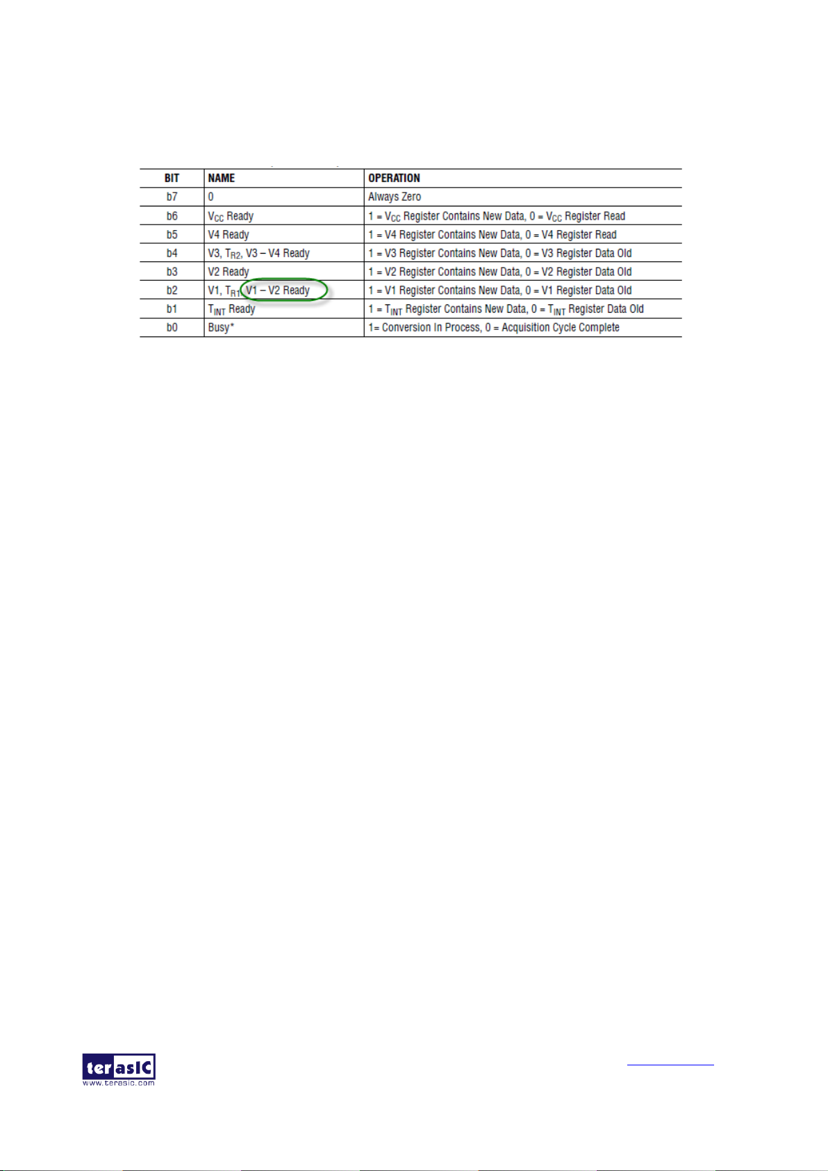
Figure 6-3 shows the register content of LTC2990. The voltage difference (V1-V2) measured are
written into two registers, MSB (register 06h) and LSB (register 07h). The most significant bit (7th
bit) of MSB register is the data_valid bit, which indicates whether the current register content has
been accessed since the result was last written to the register. This bit will be “set” i.e. 1 when the
register content is renewed and “cleared” i.e. 0 when the register content is accessed. Bit 6 of the
Page 56

MAX 10 Plus User
Manual
56
www.terasic.com
May 31, 2019
MSB register is the sign bit, Bit 5 through 0 represent the result of bits D[13:8] in two’s
complement conversion. The LSB register holds the conversion bits D[7:0]. The following
equations are used to convert the register values to get the differential voltage:
Figure 6-3 Register of LTC2990
Figure 6-4 shows the control register of LTC2990. The control register must be configured properly
to measure the voltage difference (V1-V2). Bits b[2:0] should be set to ‘110’ for measuring voltage
difference (V1-V2) and (V3-V4). Bits [4:3] should be set to 00 for all measurements.
Figure 6-4 Control Register of LTC2990
Page 57
MAX 10 Plus User
Manual
57
www.terasic.com
May 31, 2019
Figure 6-5 shows the status register of LTC2990. Bit b2 should be checked before reading the
voltage difference registers to make sure the measurement is finished and register values is the
latest for reading.
Figure 6-5 Status Register of LTC2990
◼ Design Tools
• Quartus II v15.0 64-bit
• Nios II Eclipse 15.0
◼ Demonstration Source Code
• Quartus project directory: Demonstrations\power_monitor_nios
• Nios II Eclipse project workspace: Demonstrations\power_monitor_nios\software
◼ Nios II Project Compilation
• Before you attempt to compile the reference design under Nios II Eclipse, make sure the project
is cleaned first by clicking ‘Clean’ from the ‘Project’ menu of Nios II Eclipse.
◼ Demonstration Batch File
• Demo batch file folder: Demonstrations\power_monitor_nios\demo_batch
• Batch file: test.bat
• FPGA configuration file: power_monitor_nios.sof
• Nios batch file: test.sh
• NIOS program: nios_app.elf
◼ Demonstration Setup
Please follow the procedures below to set up the demonstration:
• Please make sure Quartus II and USB-Blaster II driver are installed on the host PC.
• Connect the USB cable from the USB-Blaster II port (J8) on the MAX 10 Plus board to the host
PC.
• Power on the MAX 10 Plus board.
• Execute the demo batch file “test.bat” under the folder
Demonstrations\power_monitor_nios\demo_batch.
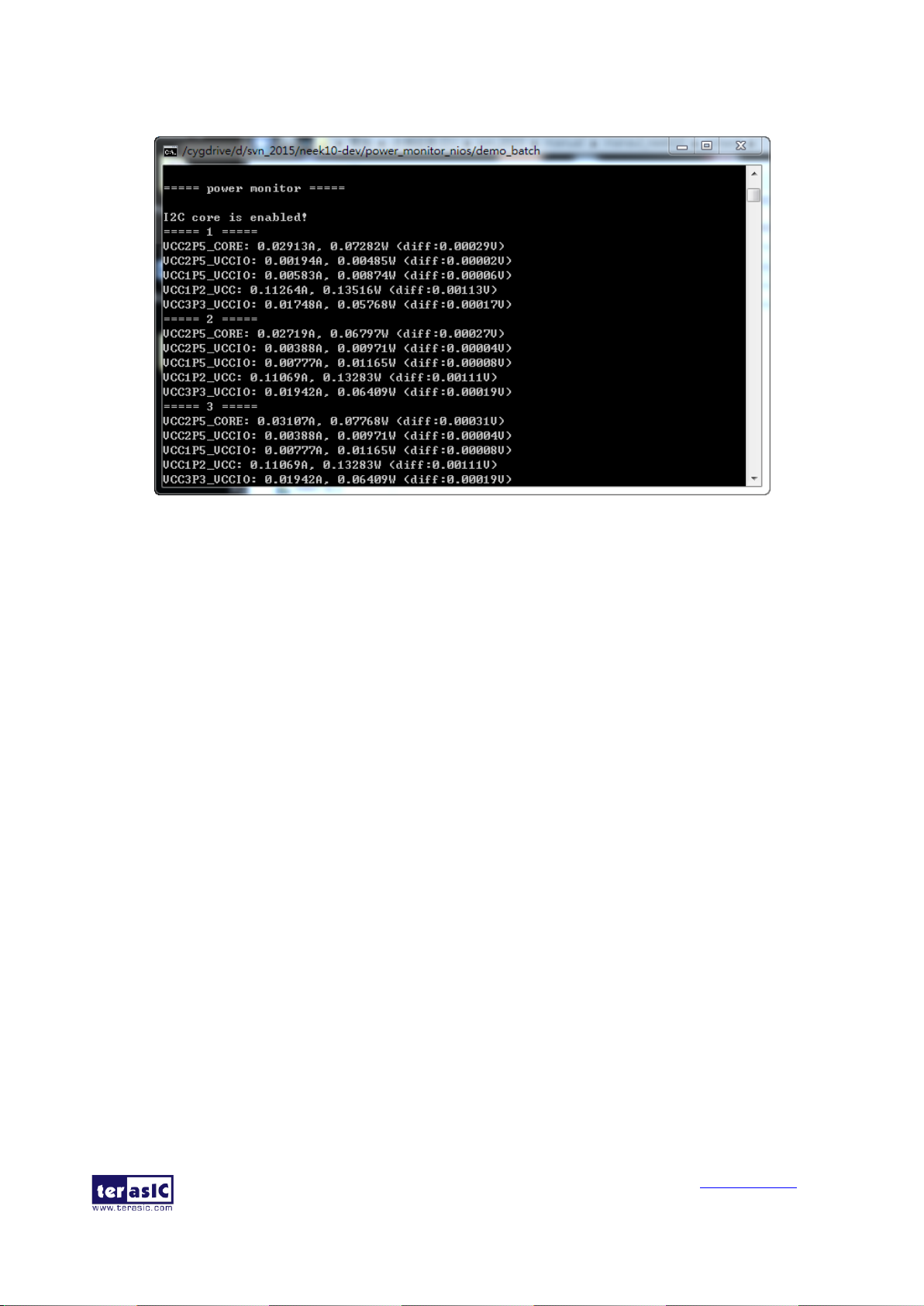
• Nios II terminal will display the measured power consumption measured, as shown in Figure
Page 58
MAX 10 Plus User
Manual
58
www.terasic.com
May 31, 2019
6-6.
Figure 6-6 Screenshot of Power_monitor_nios Demo
6.2 UART to USB Control LED
Many applications need communication with computer through common ports, the traditional
connector is RS232 which needs to connect to a RS232 cable. However, many personal computers
nowadays don't have the RS232 connector which makes it very inconvenient to develop projects.
The MAX 10 Plus board is designed to support UART communication through USB cable. The
UART to USB circuit is responsible for converting the data format. Developers can use a USB
cable rather than a RS232 cable to enable the communication between the FPGA and the host
computer. In this demonstration we will show you how to control the LEDRs by sending a
command on the computer putty terminal. The command is sent and received through a USB cable
to the FPGA. Note that in FPGA, the information was received and sent through a UART IP.
Figure 6-7 shows the hardware block diagram of this demonstration. The system requires a 50MHz
clock provided from the board. The PLL generates a 100MHz clock for Nios II processor and the
controller IP. The LEDRs are controlled by the PIO IP. The UART controller sends and receives
command data and the command is sent through Putty terminal on the computer.
Page 59

MAX 10 Plus User
Manual
59
www.terasic.com
May 31, 2019
Figure 6-7 Block Diagram of UART Control LED Demo
◼ Design Tools
• Quartus II 15.0
• Nios II Eclipse 15.0
◼ Demonstration Source Code
• Quartus Project directory: uart_usb
• Nios II Eclipse project workspace: uart_usb\software
◼ Nios II Project Compilation
• Before you attempt to compile the reference design under Nios II Eclipse, make sure the project
is cleaned first by clicking ‘Clean’ from the ‘Project’ menu of Nios II Eclipse.
◼ Demonstration Batch File
• Demo Batch File Folder: \uart_usb\demo_batch
The demo batch file includes following files:
• Batch Files: uart_usb.bat, uart_usb.sh
• FPGA Configure File: uart_usb.sof
• Nios II Program: uart_usb.elf
◼ Demonstration Setup
Please follow the procedures below to set up the demonstration:
• Connect a USB cable between your computer and the USB connector(J18) on MAX 10 Plus
board.
Page 60

MAX 10 Plus User
Manual
60
www.terasic.com
May 31, 2019
• Power on the board, if you find an unrecognized USB Serial Port in Device Manager as shown
in Figure 6-8.You should install the UART to USB driver before you run the demonstration.
Figure 6-8 Unrecognized USB Serial Port on PC
• To install UART_TO_USB driver on your computer please select the USB Serial Port to update
the driver software. The driver file can be downloaded from the following website:
http://www.ftdichip.com/Drivers/VCP.htm.
• Open the Device Manager to ensure which common port is assigned to the UART to USB port
as shown in Figure 6-9. The common number 9 (COM9) is assigned on this computer.
Figure 6-9 Check the Assigned Com Port Number On PC
• Open the putty software, type in the parameter as shown in Figure 6-10 and click open button to
open the terminal.(Here is a link for you to download the putty terminal: Download Putty)
Page 61

MAX 10 Plus User
Manual
61
www.terasic.com
May 31, 2019
Figure 6-10 Putty Terminal Setup
• Make sure Quartus II and Nios II are installed on your PC.
• Connect an USB cable to the MAX 10 Plus board (J8) and install USB Blaster driver if
necessary.
• Execute the demo batch file “uart_usb.bat” under the batch file folder uart_usb\demo_batch.
• The result of Nios II-terminal and putty terminal is shown in Figure 6-11.
Figure 6-11 Running Result of Uart_USB Demo
• In the putty terminal, type any character to change the LED state. Type a digital number to
toggle the LEDR[9..0] state and type a/A or n/N to turn on/off all LEDR.
6.3 SD Card Audio Demonstration
Many commercial media/audio players use a large external storage device, such as an SD Card or
CF card, to store music or video files. Such players may also include high-quality DAC devices
such that good audio quality can be produced. The MAX 10 Plus board provides the hardware and
Page 62
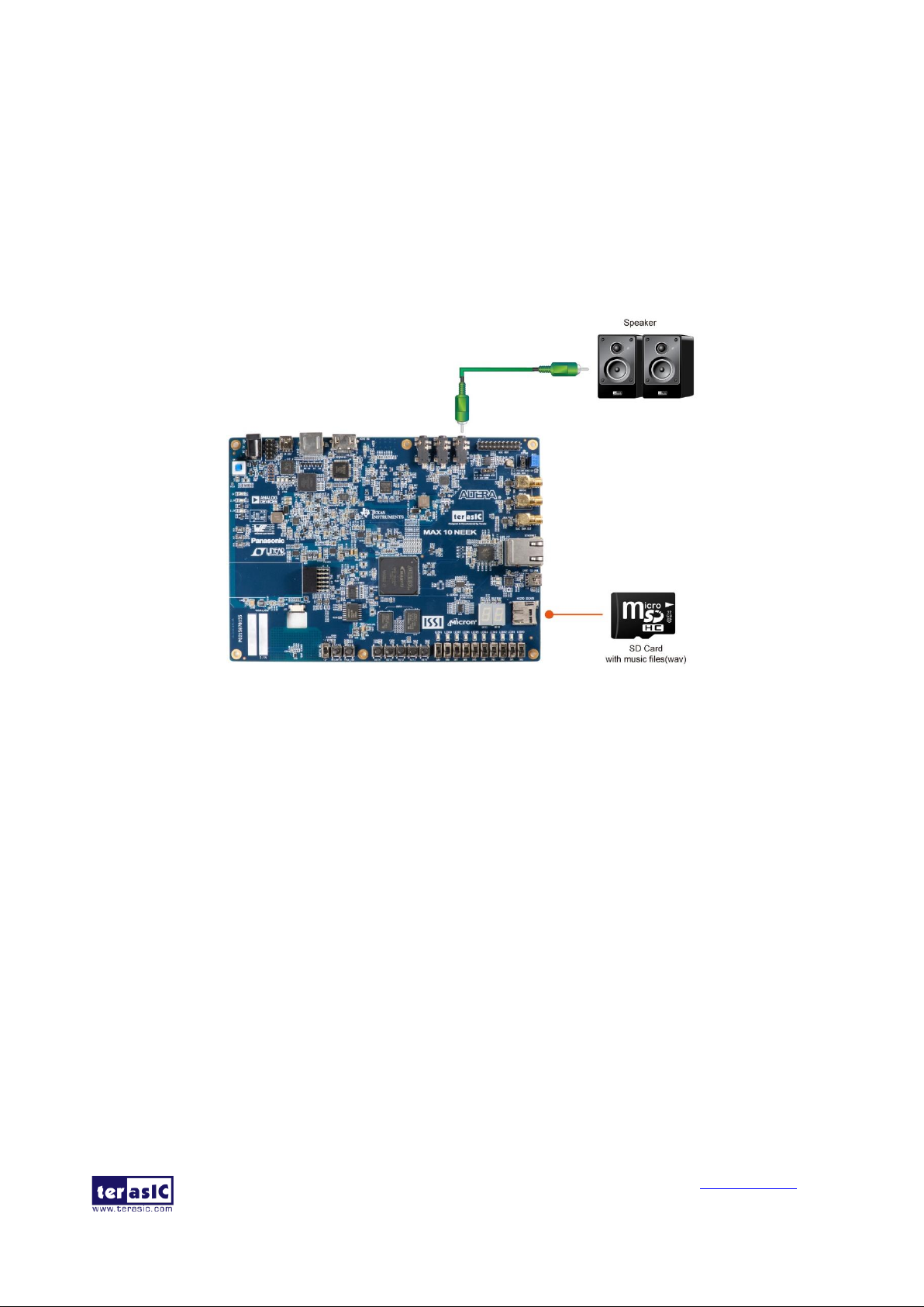
MAX 10 Plus User
Manual
62
www.terasic.com
May 31, 2019
software needed for Micro SD Card access and professional audio performance so that it is possible
to design advanced multimedia products using the MAX 10 Plus board.
Figure 6-12 shows the diagram of this demonstration. In this demonstration we show how to
implement an SD Card Music Player on the MAX 10 Plus board, in which the music files are stored
in an SD Card and the board can play the music files via its high-quality and low power audio DAC
circuits. We use the Nios II processor to read the music data stored in the SD Card and use
theTLV320AIC3254 audio CODEC to play the music.
Figure 6-12 System of SD Card Audio Demo
Figure 6-13 shows the hardware block diagram of this demonstration. The system requires a 50
MHz clock provided from the board. The PLL generates a 100MHz clock for Nios II processor and
the other controllers. The audio chip is controlled by the Audio Controller which is a user-defined
SOPC component. The internal PLL in the CODEC chip can generate the clock rate according to
the sample rate of the music. A mater clock should be supplied for the CODEC. The mater clock
rate in this demonstration is 19.2M provided by the PLL block in FPGA. The audio controller
requires the audio chip working in master mode, so the serial bit (BCLK) and the word clock
(WCLK) are provided by the audio chip. An OpenCore I2C controller is connected to the CODEC
chip for the Nios II CPU to communicate with the CODEC chip. Four PIO pins are connected to the
micro SD Card socket. SD 4-Bit Mode is used to access the micro SD Card and is implemented by
software. All the other SOPC components in the block diagram are SOPC Builder built-in
components. The PIO pins are also connected to the keys, LEDs and switches.
Page 63

MAX 10 Plus User
Manual
63
www.terasic.com
May 31, 2019
Figure 6-13 Block Diagram of SD Card Audio Demo
Figure 6-14 shows the software stack of this demonstration. SD 4-Bit Mode block implements the
SD 4-Bit mode protocol for reading raw data from the SD Card. The FAT block implements
FAT16/FAT32 file system for reading wave files that are stored in the SD Card. In this block, only
read function is implemented. The WAVE Lib block implements WAVE file decoding function for
extracting audio data from wave files. The I2C block implements I2C protocol for configuring
audio chip. The Audio block implements audio FIFO checking function and audio signal
sending/receiving function. The key and switch block acts as a control interface of the music player
system.
Figure 6-14 Software Stack of SD Card Audio Demo
Page 64

MAX 10 Plus User
Manual
64
www.terasic.com
May 31, 2019
The audio chip should be configured before sending audio signal to the audio chip. The main
program uses I2C protocol to configure the audio chip working in master mode; the audio output
interface working in I2S 16-bits per channel and with sampling rate according to the wave file
contents. In audio playing loop, the main program reads 512-byte audio data from the SD Card, and
then writes the data to DAC FIFO in the Audio Controller. Before writing the data to the FIFO, the
program will verify if the FIFO is full.
While the demonstration is running, users can get the status information through Nios II terminal.
You can adjust the volume by pressing KEY1 or KEY2. And also you can choice the song by
pressing KEY0 or KEY3.
◼ Design Tools
• Quartus II 15.0
• Nios II Eclipse 15.0
◼ Demonstration Source Code
• Quartus Project directory: sdcard_audio
• Nios II Eclipse project workspace: sdcard_audio\software
◼ Nios II Project Compilation
• Before you attempt to compile the reference design under Nios II Eclipse, make sure the project
is cleaned first by clicking ‘Clean’ from the ‘Project’ menu of Nios II Eclipse.
◼ Demonstration Batch File
Demo Batch File Folder:
• sdcard_audio\demo_batch
The demo batch file includes following files:
• Batch Files: test.bat, test.sh
• FPGA Configure File: sdcard_audio.sof
• Nios II Program: sdcard_audio.elf
◼ Demonstration Setup
Please follow the procedures below to set up the demonstration:
• Format your Micro SD Card into FAT16/FAT32 format
• Place the wave files (in folder \music) to the root directory of the Micro SD Card. The provided
wave files must have a sample rate of the following options: 96K, 48K, 44.1K or 8K. In
addition, the wave files must be stereo and 16 bits per channel.
• Connect a headset or speaker to the MAX 10 Plus board so you can hear the music played from
the micro SD Card in later.
• Insert the micro SD card into the micro SD socket on MAX 10 Plus board.
• Make sure Quartus II and Nios II are installed on your PC.
Page 65

MAX 10 Plus User
Manual
65
www.terasic.com
May 31, 2019
• Power on the MAX 10 Plus board.
• Connect an USB cable to the MAX 10 Plus board and install USB Blaster driver if necessary.
• Execute the demo batch file “test.bat” under the batch file folder sdcard_audio \demo_batch.
• Press KEY3 on the MAX 10 Plus board to play the last music file stored in the micro SD Card
and press KEY0 to play the next song.
• Press KEY2 and KEY1 to increase and decrease the output music volume respectively as shown
in Figure 6-15.
Figure 6-15 Running SD Card Audio Demo
6.4 DDR3 SDRAM Test by Nios II
Many applications use a high-performance RAM, such as a DDR3 SDRAM, to provide temporary
storage. In this demonstration hardware and software designs are provided to illustrate how to
perform DDR3 memory access in Qsys. We describe how the Altera’s “DDR3 SDRAM Controller
with UniPHY” IP is used to access a DDR3-SDRAM, and how the Nios II processor is used to read
and write the SDRAM for hardware verification. The DDR3 SDRAM controller handles the
complex aspects of using DDR3 SDRAM by initializing the memory devices, managing SDRAM
banks, and keeping the devices refreshed at appropriate intervals.
◼ System Block Diagram
Figure 6-16 shows the system block diagram of this demonstration. The system requires a 50MHz
clock provided from the board. The DDR3 controller is configured as a 128MB DDR3-300
controller. The DDR3 IP generates one 300MHz clock as SDRAM’s data clock and one half-rate
system clock 150MHz for those host controllers, e.g. Nios II processor, accessing the SDRAM. In
the Qsys, Nios II and the On-Chip Memory are designed running with the 100MHz clock, and the
Nios II program is running in the on-chip memory.
Page 66

MAX 10 Plus User
Manual
66
www.terasic.com
May 31, 2019
Figure 6-16 Block Diagram of the DDR3 Basic Demo
The system flow is controlled by a Nios II program. First, the Nios II program writes test patterns
into the whole 128MB of SDRAM. Then, it calls Nios II system function, alt_dache_flush_all, to
make sure all data has been written to SDRAM. Finally, it reads data from SDRAM for data
verification. The program will show progress in JTAG-Terminal when writing/reading data to/from
the SDRAM. When verification process is completed, the result is displayed in the JTAG-Terminal.
◼ Altera DDR3 SDRAM Controller with UniPHY
To use Altera DDR3 controller, you need to perform 4 major steps:
• Create correct pin assignments for DDR3.
• Set up correct parameters in DDR3 controller dialog.
• Perform “Analysis and Synthesis” by clicking Quartus menu: Process→Start→Start Analysis &
Synthesis.
• Run the TCL files generated by DDR3 IP by clicking Quartus menu: Tools→TCL Scripts…
◼ Design Tools
• Quartus II 15.0
• Nios II Eclipse 15.0
◼ Demonstration Source Code
• Quartus Project directory: ddr3_nios
• Nios II Eclipse Project workspace: ddr3_nios/software
◼ Nios II Project Compilation
• Before you attempt to compile the reference design under Nios II Eclipse, make sure the project
Page 67

MAX 10 Plus User
Manual
67
www.terasic.com
May 31, 2019
is cleaned first by clicking ‘Clean’ from the ‘Project’ menu of Nios II Eclipse.
◼ Demonstration Batch File
• Demo Batch File Folder: ddr3_nios\demo_batch
The demo batch folder includes following files:
• Batch Files: ddr3_nios.bat, ddr3_nios.sh
• FPGA Configure File: ddr3_nios.sof
• Nios II Program: ddr3_nios.elf
◼ Demonstration Setup
Please follow the procedures below to set up the demonstration:
• Make sure Quartus II and Nios II are installed on your PC.
• Power on the MAX 10 Plus board.
• Use an USB cable to connect PC and the MAX 10 Plus board (J8) and install USB Blaster
driver if necessary.
• Execute the demo batch file “ddr3_nios.bat” for USB-Blaster II under the batch file folder,
ddr3_nios\demo_batch
• After Nios II program is downloaded and executed successfully, a prompt message will be
displayed in Nios2-terminal.
• Press KEY4~KEY0 of the MAX 10 Plus board to start SDRAM verify process. Press KEY0 for
continued test.
• The program will display progress and result information, as shown in Figure 6-17.
Figure 6-17 Display Progress and Result Information for the DDR3 Demo
Page 68

MAX 10 Plus User
Manual
68
www.terasic.com
May 31, 2019
6.5 Ethernet Socket server
This design example demonstrates a socket server using the sockets interface of the NicheStack™
TCP/IP Stack Nios II Edition with MicroC/OS-II to serve socket connection to the MAX 10 Plus
board. The server can continuously listen for commands on a TCP/IP port and operate the MAX 10
Plus LEDs according to the commands from the telnet client.
As Part of the Nios II EDS, NicheStack™ TCP/IP Network Stack is a complete networking
software suite designed to provide an optimal solution for network related applications
accompanying Nios II.
Also to understand how this demo works, we assume that you already have a basic knowledge of
TCP/IP protocols. As indicated in the block diagram in Figure 6-18, the Nios II processor is used to
communicate with the Client via 88E1111(RGMII/MII interface)Ethernet Device.
Figure 6-18 Block Diagram
We will now cover the Qsys system in this demo which contains Nios II processor, DDR3 memory,
JTAG UART, timer, Triple-Speed Ethernet, Scatter-Gather DMA controller and other peripherals
etc. In the Core Configuration Tab of the Altera Triple-Speed Ethernet Controller, users need to set
the MAC interface as RGMII as shown in Figure 6-19.
Page 69

MAX 10 Plus User
Manual
69
www.terasic.com
May 31, 2019
Figure 6-19 Select RGMII Interface under MAC Configuration
In the MAC Options tab (See Figure 6-20), users should set up proper values for the PHY chip
88E1111. The MDIO Module should be included, as it is used to generate a 2.5MHz MDC clock for
the PHY chip from the controller's source clock (here a 100MHz clock source is expected) to divide
the MAC control register interface clock to produce the MDC clock output on the MDIO interface.
The MAC control register interface clock frequency is 100MHz and the desired MDC clock
frequency is 2.5MHz, so a host clock divisor of 40 should be used.
Page 70

MAX 10 Plus User
Manual
70
www.terasic.com
May 31, 2019
Figure 6-20 MAC Options Configuration
Once the Triple-Speed Ethernet IP configuration has been set and necessary hardware connections
have been made as shown in Figure 6-21, click on generate.
Figure 6-21 Qsys Builder
Page 71

MAX 10 Plus User
Manual
71
www.terasic.com
May 31, 2019
Figure 6-22 shows the connections for programmable 10/100/1000Mbps Ethernet operation via
RGMII.
Figure 6-22 PHYConnected to the MAC via RGMII
After the Qsys hardware project has been built, develop the Qsys software project, whose basic
architecture is shown in Figure 6-23. The top block contains the Nios II processor and the
necessary hardware to be implemented into the MAX 10 Plus board. The software device drivers
contain the necessary device drivers needed for the Ethernet and other hardware components to
work. The HAL API block provides the interface for the software device drivers, while the Micro
C/OS-II provides communication services to the NicheStack™ and the Socket Server. The
NicheStack™ TCP/IP Stack software block provides networking services to the application block
where it contains the tasks for Socket Server and also LED management.
Page 72

MAX 10 Plus User
Manual
72
www.terasic.com
May 31, 2019
Figure 6-23 Nios II Software Routine Architecture
Finally, the detailed descriptions for Software flow chart of the Socket Server program are listed
below:
Firstly, the Socket Server program initiates the MAC and net device then calls the get_mac_addr()
function to set the MAC addresses for the PHY. Secondly, it initiates the auto-negotiation process to
check the link between the PHY and gateway device. If the link exists, the PHY and gateway
devices will broadcast their transmission parameters, speed, and duplex mode. After the
auto-negotiation process has been finished, the link will be established. Next, the Socket Server
program will prepare the transmitting and receiving path for the link. If the path is created
successfully, it will call the get_ip_addr() function to set up the IP address for the network interface.
After the IP address is successfully distributed, the NicheStack™ TCP/IP Stack will start to run for
Socket Server application.
Note: your gateway should support DHCP because it uses DHCP protocol to request a valid
IP from the Gateway, or else you would need to reconfigure the system library to use static IP
assignment.
◼ Design Tools
• Quartus II v15.0
• Nios II Eclipse 15.0
Page 73

MAX 10 Plus User
Manual
73
www.terasic.com
May 31, 2019
◼ Demonstration Source Code
• Project directory: socket_server
• Nios II Eclipse Project workspace: socket_server/software
◼ Demonstration Batch File
• Demo batch file folder: Demonstrations/socket_server /demo_batch/
• Batch file: socket_server.bat
• FPGA configure file: socket_server.sof
• Application file folder: socket_server /demo_batch/
• Application file: open_telnet.bat
◼ Demonstration Setup
Please follow the procedures below to set up the demonstration:
• Please make sure both Quartus II and USB-Blaster II driver are installed on the host PC.
• Connect the USB cable from the USB-Blaster II port (J8) on the MAX 10 Plus board to the host
PC.
• Power on the MAX 10 Plus board.
• Execute the demo batch file “socket_server.bat” under the folder Demonstrations/socket_server
/demo_batch , then the IP address and port number are assigned as shown below in Figure 6-24.
Figure 6-24 Simple Socket Server
• To establish connection, start the telnet client session by executing open_telnet.bat file and
include the IP address assigned by the DHCP server-provided IP along with the port number as
Page 74
MAX 10 Plus User
Manual
74
www.terasic.com
May 31, 2019
shown below in Figure 6-25.
Figure 6-25 Telnet Client
Note: If you can’t open the open_telnet.bat file, please try to set the Telnet Client feature as
following screenshot:
• From the Simple Socket Server Menu, enter the commands in the telnet session. Entering a
number from zero through seven, followed by a return, causes the corresponding LEDRs
(D0-D7) to toggle on or off on the MAX 10 Plus board as shown below in Figure 6-26.
Page 75

MAX 10 Plus User
Manual
75
www.terasic.com
May 31, 2019
Figure 6-26 Display Progress and Result Information for the Socket Server Demonstration
6.6 Digital Accelerometer Demonstration
This demonstration shows a bubble level implementation based on a digital accelerometer. We use
I2C protocol to control the ADXL345 digital accelerometer, and the APDS-9301 Miniature Ambient
Light Photo Sensor. The Nios II Console displays the reuslt of our demo. When tilting the MAX 10
Plus, the ADXL345 measures the static acceleration of gravity. In our Nios II software, we compute
the change of angle in the x-axis and y-axis, and show the angle data on the Nios II Console. The
value of light sensor will change as the brightness changes around the light sensor.
Figure 6-27 shows the hardware system block diagram of this demonstration. The system is
clocked by an external 50MHz Oscillator. Through the internal PLL module, the generated 100MHz
clock is used for Nios II processor and other components, and there is also 40MHz for low-speed
peripherals.
Figure 6-27 Block Diagram of the Digital Accelerometer Demonstration
◼ Demonstration Source Code
• Project directory: gsensor_lightsensor
• Bit stream used: gsensor_lightsensor.sof
Page 76

MAX 10 Plus User
Manual
76
www.terasic.com
May 31, 2019
• Nios II Eclipse project workspace: gsensor_lightsensor \software
◼ Demonstration Batch File
• Demo Batch File Folder: gsensor_lightsensor \demo_batch
The demo batch file includes the following files:
• Batch File: gsensor_lightsensor.bat, gsensor_lightsensor.sh
• FPGA Configure File: gsensor_lightsensor.sof
• Nios II Program: gsensor_lightsensor.elf
◼ Demonstration Setup
Please follow the procedures below to set up the demonstration:
• Load the bit stream into the FPGA on the MAX 10 Plus board.
• Run the Nios II Software under the workspace gsensor_lightsensor\software (Note*).
• After the Nios II program is downloaded and executed successfully, a prompt message will be
displayed in Nios2-terminal: “its ADXL345’s ID = e5”.
• Tilt the MAX 10 Plus to all directions, and you will find that the angle of the g-sensor and value
of light sensor will change. Figure 6-28 shows the demonstration result.
Figure 6-28 Digital Accelerometer Demonstration
Note: Execute gsensor_lightsensor_\demo_batch\gsensor_lightsensor.bat to download .sof
and .elf files.
Page 77
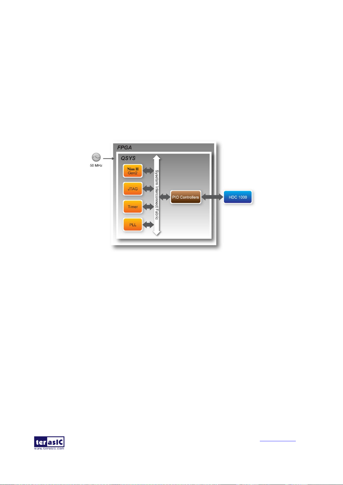
MAX 10 Plus User
Manual
77
www.terasic.com
May 31, 2019
6.7 Humidity/Temperature Sensor
This demonstration illustrates steps to evaluate the performance of humidity and temperature sensor
HDC1000. The HDC1000 is a fully integrated humidity and temperature sensor, providing excellent
measurement accuracy and long-term stability. Humidity and temperature results can be read out
through the I2C compatible interface. The Nios II Console displays the result of our demo. In our
Nios II software, we show temperature and humidity data on the Nios II Console. The value of the
sensor will change as the environment changes.
Figure 6-29 shows the block diagram of this demonstration. In this demonstration, a Nios II
processor is used to achieve i2c operation and display results on the Nios II console.
Figure 6-29 Block Diagram of Humidity and Temperature Sensor
This demonstration shows basic function of HDC1000 and temperature and humidity reading in
different acquisition modes. HDC1000 can perform measurements of both humidity and
temperature, or either humidity only or temperature only. The measurement resolution can be set to
8, 11, or 14 bits for humidity; 11 or 14 bits for temperature. Different resolution setting results in a
different conversion time. When triggering the measurements, operation should wait for the
measurements to complete based on the conversion time. Alternatively, wait for the assertion of
DRDYn. In this demonstration, a delay in I2C function is adopted to simplify the process.
◼ Design Tools
• Quartus II v15.0
• Nios II Eclipse 15.0
◼ Demonstration Source Code
• Quartus project directory: humidity_temperature
• Nios II Eclipse project workspace: humidity_temperature \software
Page 78

MAX 10 Plus User
Manual
78
www.terasic.com
May 31, 2019
◼ Demonstration File Locations
• Hardware project directory: humidity_temperature
• Bitstream used: humidity_temperature.sof
• Software project directory: humidity_temperature \software
• Demo batch file: humidity_temperature \demo_batch\ humidity_temperature.bat
◼ Demonstration Setup and Instructions
Please follow the procedures below to set up the demonstration:
• Make sure Quartus II and USB-Blaster II driver are installed on your PC.
• Connect the USB cable to the USB Blaster II connector (J8) on the MAX 10 Plus board and
host PC.
• Power on the MAX 10 Plus board.
• Execute the demo batch file “humidity_temperature.bat” under the batch file folder,
humidity_temperature\demo_batch.
• NIOS terminal and will display the humidity and temperature values. Figure 6-30 shows the
demonstration result.
Figure 6-30 Humidity and Temperature Sensor Demo
Page 79
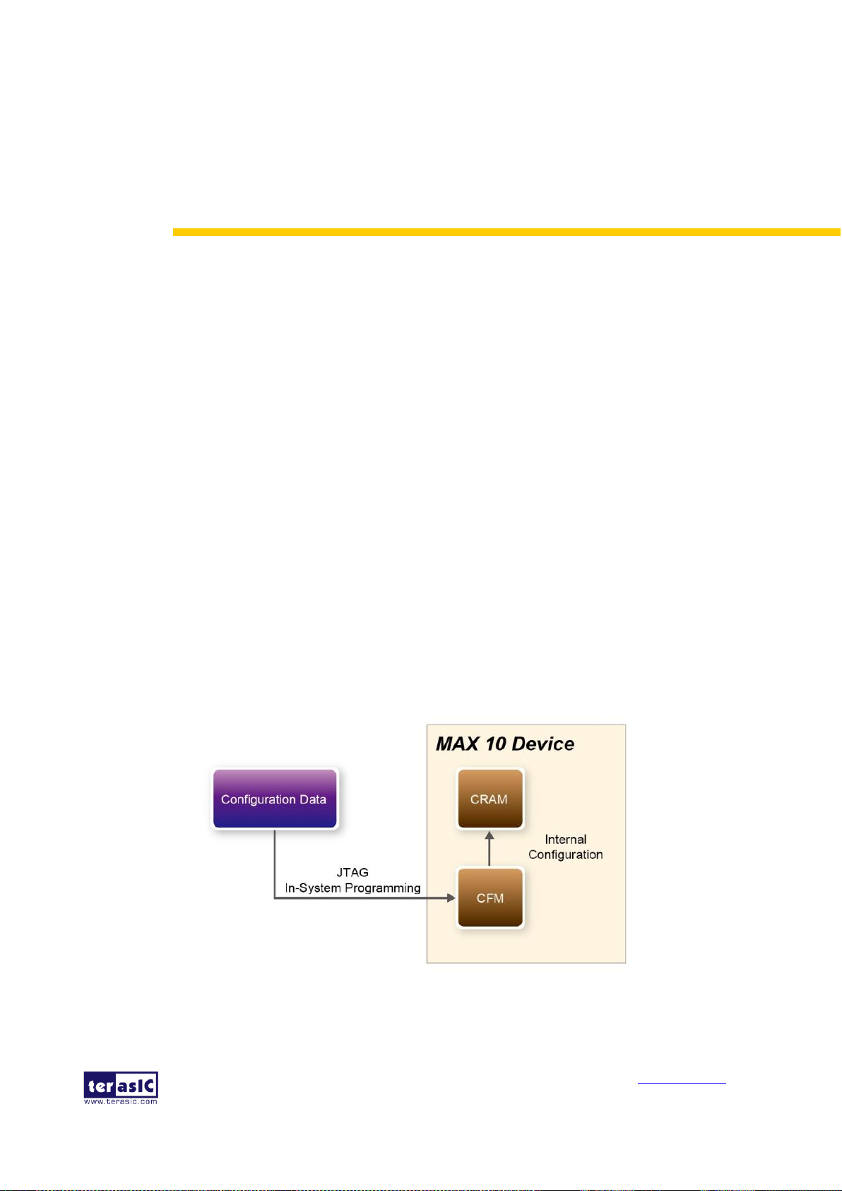
MAX 10 Plus User
Manual
79
www.terasic.com
May 31, 2019
Chapter 7
Programming the Configuration
Flash Memory
This tutorial provides comprehensive information that will help you understand how to configure
MAX 10 Plus Board using internal configuration mode. The MAX 10 device on MAX 10 Plus Board
supports dual image boot. This tutorial explains the details of the dual image boot. The following
sections provide a quick overview of the design flow.
7.1 Internal Configuration
The internal configuration scheme for all MAX 10 devices except for 10M02 device consists of the
following mode:
• Dual Compressed Images—configuration image is stored as image0 and image1 in the
configuration flash memory (CFM).
• Single Compressed Image.
• Single Compressed Image with Memory Initialization.
• Single Uncompressed Image.
• Single Uncompressed Image with Memory Initialization.
In dual compressed images mode, you can use the BOOT_SEL pin to select the configuration
image.
The High-Level Overview of Internal Configuration for MAX 10 Devices as shown in Figure 7-1.
Figure 7-1 High-Level Overview of Internal Configuration for MAX 10 Devices
Page 80

MAX 10 Plus User
Manual
80
www.terasic.com
May 31, 2019
Before internal configuration, we need to program the configuration data into the configuration
flash memory (CFM). The CFM will be part of the programmer object file (.pof) programmed into
the internal flash through the JTAG In-System Programming (ISP).
During internal configuration, MAX 10 devices load the configuration RAM (CRAM) with
configuration data from the CFM. Both of the application configuration images, image 0 and image
1, are stored in the CFM. The MAX 10 device loads either one of the application configuration
image from the CFM. If an error occurs, the device will automatically load the other application
configuration image. Remote System Upgrade Flow for MAX 10 Devices is shown in Figure 7-2.
Figure 7-2 Remote System Upgrade Flow for MAX 10 Devices
The operation of the remote system upgrade feature detecting errors is as follows:
1. After powering-up, the device samples the BOOT_SEL pin to determine which application
configuration image to boot. The BOOT_SEL pin setting can be overwritten by the input register of
the remote system upgrade circuitry for the subsequent reconfiguration.
2. If an error occurs, the remote system upgrade feature reverts by loading the other application
configuration image. The following lists the errors that will cause the remote system upgrade
feature to load another application configuration image:
• Internal CRC error
• User watchdog timer time-out
3. Once the revert configuration completes and the device is in the user mode, you can use the
remote system upgrade circuitry to query the cause of error and which application image failed.
4. If a second error occurs, the device waits for a reconfiguration source. If the auto-reconfig is
enabled, the device will reconfigure without waiting for any reconfiguration source.
5. Reconfiguration is triggered by the following actions:
• Driving the nSTATUS low externally
• Asserting internal or external nCONFIG low
Page 81

MAX 10 Plus User
Manual
81
www.terasic.com
May 31, 2019
• Asserting RU_nCONFIG low
7.2 Using Dual Compressed Images
The internal configuration scheme for all MAX 10 devices except for 10M02 device consists of the
following mode:
• Dual Compressed Images—configuration image is stored as image 0 and image 1 in the
configuration flash memory (CFM).
• Single Compressed Image.
This section will just introduce how to use MAX10 device Dual Compressed Images feature. If you
don’t need this feature, skip this section
Two main steps are necessary for a project support dual configuration mode.
• Add dual configuration IP.
• Modify Configuration Mode in device setting.
A Dual Configuration IP should be added in an original project, so that the .pof file can be
programmed into CFM through it.
• Open Quartus project and choose Tools > Qsys to open Qsys system wizard. Create a new
system and add the dual configuration IP. Connect the logic as Figure 7-3.
Figure 7-3 Rename and Connect Dual Boot IP
• Save the Qsys as dual_boot.qsys and generate the HDL files. Add the dual_boot.qip into the
quartus setting file and add the qsys instance in the top design file as shown in Figure 7-4.
Page 82
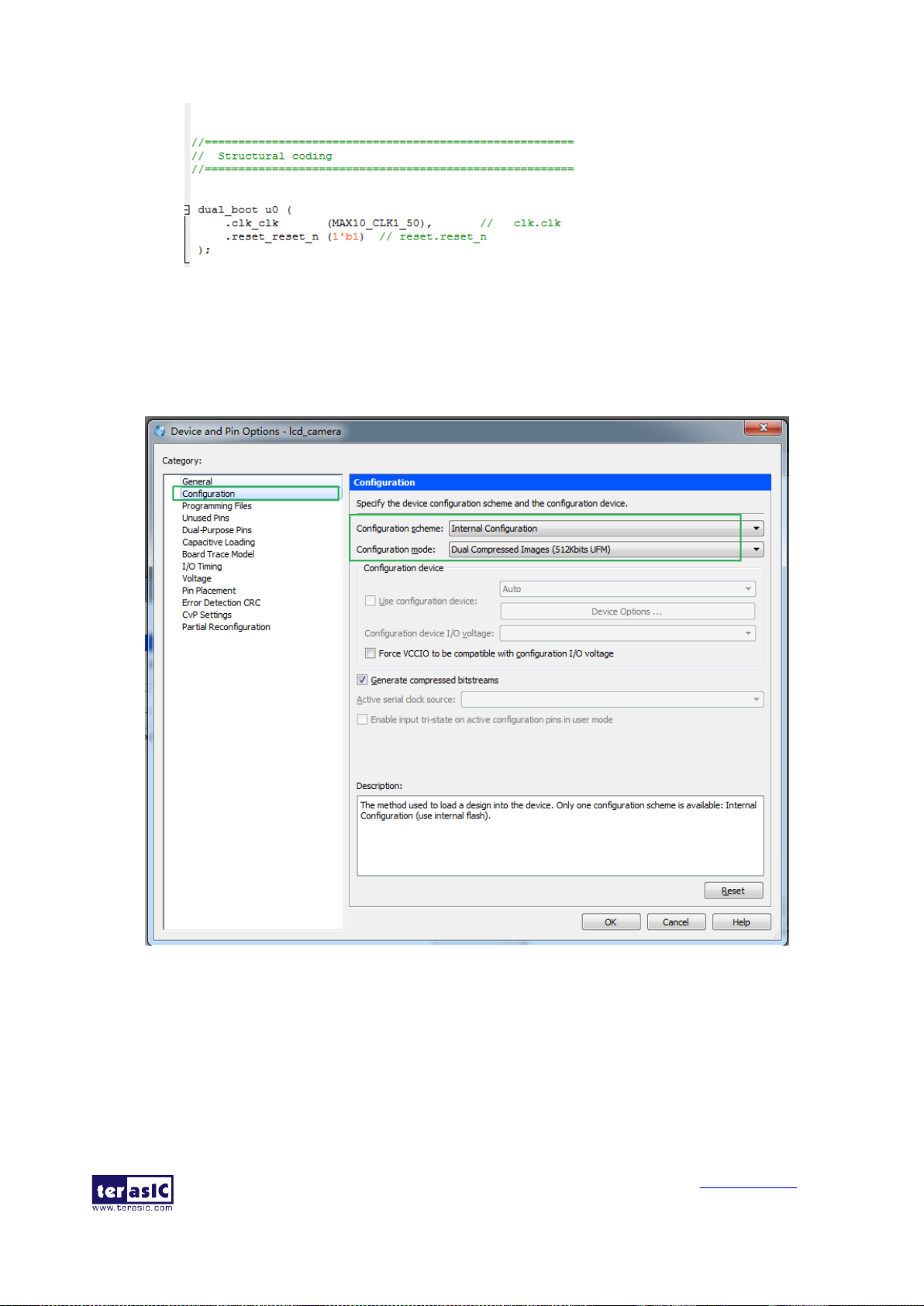
MAX 10 Plus User
Manual
82
www.terasic.com
May 31, 2019
Figure 7-4 Add the Qsys Instance in Top
• The configuration mode is set in Device and Pin Options window. Choose Assignments >
Device to open Device windows. Click the Device and Pin Options and choose Dual
Compressed Images in configuration table as shown in Figure 7-5. Then compile the project to
generate the sof file.
Figure 7-5 Set Dual Configuration Modes
These procedures should be implemented in both projects for dual boot.
• The next step is to convert the two sof files into a pof file for programming the MAX10 FPGA.
Open the convert programming Files tool in Quartus and set as Figure 7-6.
Page 83

MAX 10 Plus User
Manual
83
www.terasic.com
May 31, 2019
Figure 7-6 Convert File Window Setting
• In the Input files to convert table, click Add File button to choose the sof file for image0. Then
press the Add Sof Page button and add a sof for image1 as shown in Figure 7-7. Click generate
button to generate the object file—dual_boot.pof.
Figure 7-7 Add Sof Files
• The final step is to download the pof into MAX10 FPGA. Open the programmer tool and add
the dual_boot.pof as shown in Figure 7-8. Click Start button to program the device when the
hardware is set OK.
Figure 7-8 Download the pof
Page 84

MAX 10 Plus User
Manual
84
www.terasic.com
May 31, 2019
• Now, you can set the BOOT_SEL by SW16, you will find if you set BOOT_SEL=0, the image0
will be loaded and if you set BOOT_SEL=1, he image1 will be loaded.
7.3 Nios II Load In Single Boot Image
After the internal configuration, if a Nios II processor is contained in the image and the reset vector
of the processor is set to onchip memory data section, the CPU will load the code from the UFM in
the onchip flash. The CPU loading procedure occurs either in single image configuration mode or
dual compressed image configuration mode. You must make sure only one image contains the
processor in dual compressed image configuration mode.
Users need to write the hardware and software binary into the nonvolatile flash memory for the
MAX10 FPGA auto boot after power-cycling. The onchip flash memory in the FPGA provides the
possibility to boot the software for the Nios II processor.
The demonstration my_first_niosII is designed for Nios II processor loading software after the
FPGA configuration complete. The section describes the detailed steps of the design.
• An onchip flash controller ip should be added into the Qsys for storing software code. The CPU
data master and instruction master interface are connected to the onchip flash data bus as shown
in Figure 7-9.
Figure 7-9 Qsys Design
• And the reset vector of the CPU should be onchip flash data section. The configuration mode in
the onchip flash parameter setting and the Quartus device setting window should all be set as
Single Uncompressed Image.
• In the BSP Editor (Nios II SBT for Eclipse) utility of the Eclipse, all the check box in the
hal.linker table should be checked as shown in Figure 7-10.
Figure 7-10 BSP Advance Setting
Page 85

MAX 10 Plus User
Manual
85
www.terasic.com
May 31, 2019
• Make sure you have set your software’s program memory (.text section) in onchip Flash
memory through BSP Editor (Nios II SBT for Eclipse) utility.
• Compile the target into initial flash format by choosing the mem_init_generate option in the
Make Target window in Eclipse as shown in Figure 7-11.
Figure 7-11 Make Target Setting
• After clicking build button, a onchip_flash hex file will be generated in the path
software\software_project\mem_init.
• Open the convert programming file window in Quartus II and set the window as shown in
Figure 7-12.
Figure 7-12 Convert File Window Setting
• Click the Options/Boot info… button. Choose the UFM source as the load memory file and
click browse button to open the onchip flash hex file as shown in Figure 7-13. Press OK button
to close the window.
Page 86

MAX 10 Plus User
Manual
86
www.terasic.com
May 31, 2019
Figure 7-13 Add Hex Data Window
• In the Input files to convert table, choose the sof and generate the pof.
• Open the programmer tool and add the pof generated above to download into the onchip flash.
Power cycle the board, the Nios II software will be running after the image has been loaded.
Page 87

MAX 10 Plus User
Manual
87
www.terasic.com
May 31, 2019
Chapter 8
Appendix
8.1 Revision History
Version
Change Log
V1.0
Initial Version
8.2 Copyright Statement
Copyright ©Terasic Inc. All rights reserved.
 Loading...