

Page 1

Page 2

- 1 -
HDMI-FMC_User_Manual www.terasic.com
August 6, 2019
Chapter 1 HDMI-FMC Development Kit ......................................... 2
1-1 Package Contents .......................................................... 3
1-2 HDMI-FMC System CD ............................................... 3
1-3 Getting Help .................................................................. 3
Chapter 2 Introduction of the HDMI-FMC Card ............................ 4
2-1 Features ......................................................................... 5
2-2 Block Diagram of the HDMI-FMC Board .................... 7
2-3 Connectivity .................................................................. 8
Chapter 3 Using the HDMI-FMC Board ....................................... 10
3-1 Sil9136-3 ..................................................................... 10
3-2 ADV7619 .................................................................... 26
3-3 Level shift .................................................................... 27
3-4 FMC Connector ........................................................... 29
Chapter 4 Example Codes ............................................................... 34
4-1 4K HDMI Loopback Demonstration ........................... 34
Chapter 5 Appendix ......................................................................... 45
Page 3

- 2 -
HDMI-FMC_User_Manual www.terasic.com
August 6, 2019
Chapter 1
HDMI-FMC Development Kit
Terasic HDMI-FMC is a HDMI transmitter/receiver daughter board with FMC (FPGA Mezzanine
card) interface. The user can connect the HDMI module with the FPGA development kit via the FMC
connector for HDMI image & video capture, processing and display up to 4K@30fps resolution.
The HDMI-FMC provides both the HDMI Tx and Rx Module with the HDMI 1.4a features supported.
The Tx module is able to supports most common standard and non-standard video input format, most
common 3D formats and the video resolution up to 8-bit 4K(30Hz)、12-bit 1080p(60Hz)、12-bit
720p/1080i (120 Hz),and 16-bit 1080p (30 Hz). The audio interface supports S/PDIF, DSD, I2S and
HBR audio format input.
The Rx module is able to support all mandatory and additional 3D video formats and extended
colorimetry (sYCC601, Adobe® RGB, Adobe YCC601, xvYCC extended gamut color CEC
1.4-compatible) with up to 36-bit Deep Color. the audio interface supports S/PDIF, SACD, DSD, I2S
and HBR audio format output.
We also provide complete demo source codes for the HDMI-FMC working with different FPGA
development kits. These demos are created by using Verilog HDL & ALTERA VIP, by referring to
these demos, users can quickly develop their own applications.
Page 4

- 3 -
HDMI-FMC_User_Manual www.terasic.com
August 6, 2019
1-1 Package Contents
Figure 1-1 The HDMI-FMC package contents
The HDMI-FMC package includes:
⚫ One HDMI-FMC module
⚫ Screw & Copper Pillar Package
⚫ System CD Download Guide
1-2 HDMI-FMC System CD
The HDMI-FMC System CD contains all the documents and supporting materials associated with
HDMI-FMC, including the user manual, reference designs, and device datasheets. Users can
download this system CD from the link: http://hdmi-fmc.terasic.com/cd.
1-3 Getting Help
Here are the addresses where you can get help if you encounter any problems:
Terasic Technologies
9F., No.176, Sec.2, Gongdao 5th Rd, East Dist, Hsinchu City, 30070. Taiwan
Email: support@terasic.com
Tel.: +886-3-575-0880
Website:http://www.terasic.com
Page 5

- 4 -
HDMI-FMC_User_Manual www.terasic.com
August 6, 2019
Chapter 2
Introduction of the HDMI-FMC Card
This chapter describes the architecture and configuration of the HDMI-FMC Board including block
diagram and components related.
Figure 2-1 The HDMI-FMC Board PCB and Component Diagram of top side
The Photographs of the HDMI-FMC are shown in Figure 2-1 and Figure 2-2. They depict the
layout of the board and indicates the location of the connectors and the key components on the top
and bottom side.
Page 6

- 5 -
HDMI-FMC_User_Manual www.terasic.com
August 6, 2019
Figure 2-2 The HDMI-FMC Board PCB and Component Diagram of bottom side
The following components are provided on the HDMI-FMC Board:
⚫ HDMI TX chip SiI9136-3
⚫ HDMI TX chip ADV7619
⚫ LEVEL Shift EPM2210
⚫ FMC Connector (HPC)
2-1 Features
The HDMI-FMC card has many features that allow users to implement a wide range of design
circuits, from simple circuits to various multimedia projects.
The following hardware is provided on the board:
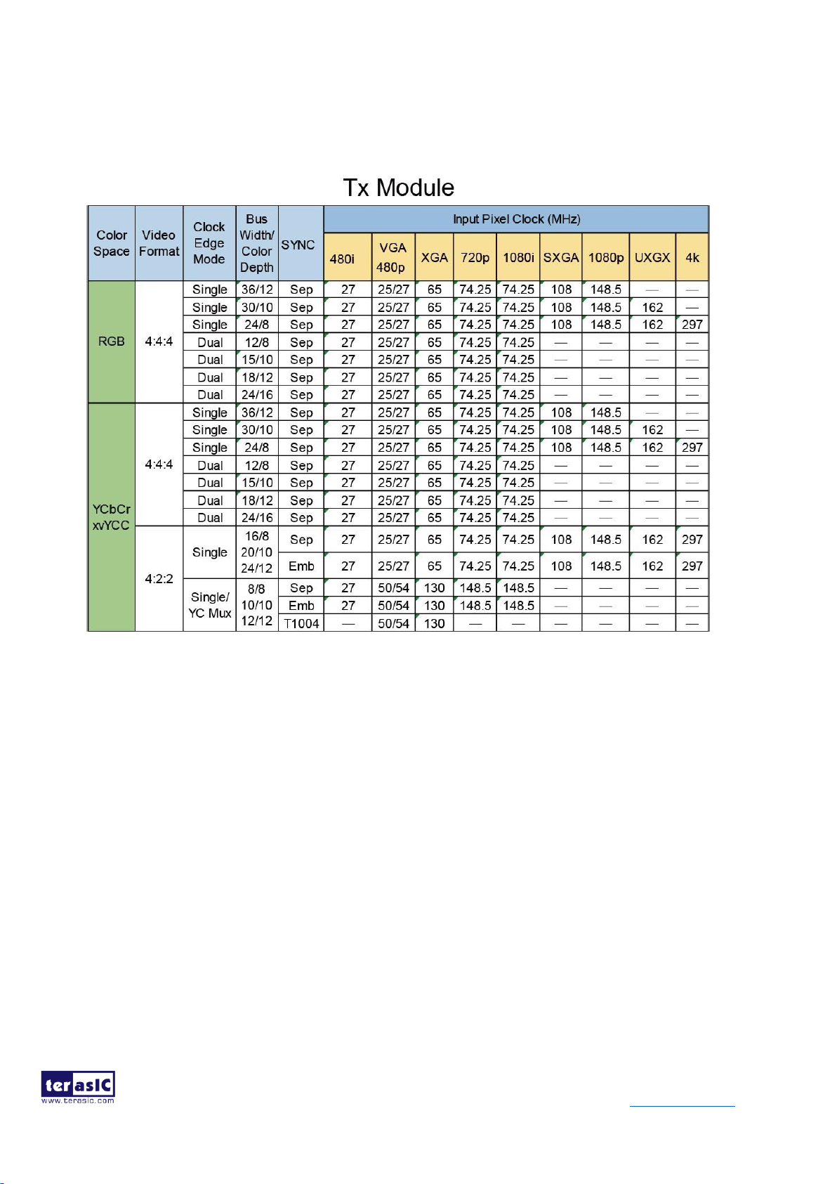
Package Interface:VITA 57.1 FMC, adjustable I/O-standard(1.5/1.8/2.5/3.0V).
Tx Module:
Page 7
- 6 -
HDMI-FMC_User_Manual www.terasic.com
August 6, 2019
⚫ Chip P/N:SiI9136-3
⚫ HDMI 1.4a/1.3, HDCP 1.4 and DVI Compliant
⚫ Video formats:4:4:4 RGB, 4:4:4/4:2:2 YCbCr
⚫ Pixels resolution:4Kx2K@30Hz
⚫ Pixels clock:DDR/SDR up to 300MHz
⚫ 3D format support
⚫ High Bitrate Audio support
Page 8

- 7 -
HDMI-FMC_User_Manual www.terasic.com
August 6, 2019
Rx Module:
⚫ Chip P/N: ADV7619
⚫ HDMI 1.4a/1.3, HDCP 1.4 and DVI Compliant
⚫ Video formats: 4:4:4 RGB, 4:4:4/4:2:2 YCbCr
⚫ Pixels resolution: 3840x2160@30Hz
⚫ Pixels clock: DDR/SDR up to 297MHz
Level Shift:
⚫ EPM2210
⚫ I/O-Standard (1.5/1.8/2.5/3.0V)
2-2 Block Diagram of the HDMI-FMC Board
Below Figure 2-3 shows the HDMI-FMC Block Diagram. Level shift module outputs audio and
video image data from FMC connector, which can be converted to TMDS data by passing through the
Sil9136-3 to the HDMI TX connector. Similarly, HDMI RX connector receives all mandatory 3D TV
formats defined in the HDMI 1.4a specification through a dual input HDMI-capable, which can be
converted to audio and video image data by the ADV7619,and send to the FMC connector through
Level shift. Both Sil9136-3 and ADV7619 can be controlled by FPGA I2C interface.
Figure 2-3 Block Diagram of the HDMI-FMC Board
Page 9

- 8 -
HDMI-FMC_User_Manual www.terasic.com
August 6, 2019
2-3 Connectivity
Terasic HDMI-FMC is able to connect on to any FPGA development kit equiped with FMC
(High-Pin Count) connector. The Below pictures Figure 2-4, Figure 2-5 and Figure 2-6 show the
connections with three different Terasic FPGA Boards:
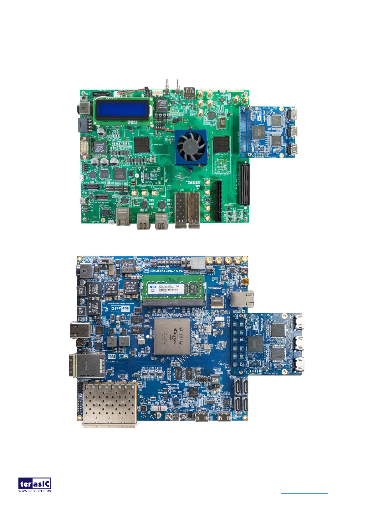
Figure 2-4 Connect the HDMI-FMC to TR5 board’s FMCD port
Page 10
- 9 -
HDMI-FMC_User_Manual www.terasic.com
August 6, 2019
Figure 2-5 Connect the HDMI-FMC to A10SoC board’s FMCA port
Figure 2-6 Connect the HDMI-FMC to Terasic HAN Pilot Platform FMC port
Page 11

- 10 -
HDMI-FMC_User_Manual www.terasic.com
August 6, 2019
Chapter 3
Using the HDMI-FMC Board
This chapter provides instructions on how to use Sil9136-3, ADV7619, Level shift and FMC
connector on the HDMI-FMC board.
3-1 Sil9136-3
Sil9136-3 is a HDMI Deep Color transmitter and can deliver up to 16-bit Deep Color at 1080p/30Hz
resolutions and 12-bit Deep Color at 1080p/60Hz resolutions. It merge independent video and audio
streams for transmission over HDMI. For video data input, Sil9136-3 support most standard and
non-standard video input formats and resolutions up to 8-bit 4K/30Hz, 12-bit 1080p/60Hz, 12-bit
720p/120 Hz, 12-bit 1080i/120 Hz, and 16-bit 1080p/30Hz. For audio input, it supports I2S, Direct
Stream Digital, and S/PDIF audio input formats.
For HDMI output, DVI and HDMI transmitter with xvYCC extended color gamut, Deep Color up to
16-bit color, and high bitrate audio are all supported. The I2C address for TPI/CR of Sil9136-3 is
0x72/0x7A. Figure 3-1 shows the system block diagram of Sil9136-3.
Figure 3-1 Sil9136-3 HDMI transmitter
The Sil9136-3 transmitter has four GPIO pins, and the value of each pin can be read or set through
the local I2C bus. The sil9136-3 also contains a Consumer Electronics Control (CEC) interface which
incorporates an HDMI-compliant CEC I/O and the Lattice CEC Programming Interface (CPI); this
reduces the need for system-level control by the system microcontroller and simplifies firmware
overhead.
Page 12

- 11 -
HDMI-FMC_User_Manual www.terasic.com
August 6, 2019
There are individual components processing the video and audio input data. In the video data input
and conversion block, the bus configurations support most standardized video input formats as well
as other widely used non-standard formats. After configuration and processing, the clock, data, and
sync information are combined into a complete set of signals required for further processing as
follows. The upsampler and downsampler block convert the 4:2:2 sampled video to 4:4:4 and 4:4:4
sampled video to 4:2:2 seperately. The two color space converters (CSCs, convert YCbCr to RGB and
RGB to YCbCr) are available to interface to the many video formats supplied by A/V processors and
provide full DVI backward compatibility. RGB range expression block scales the input color range
from limited-range into full-range and RGB/YCbCr range compression compresses full-range data
into limited-range data for each video channel. The clipping and dither function are also employed in
the transmitter. The audio capture block supports I2S, Direct Stream Digital, and S/PDIF audio input
formats. The appropriate registers must be configured to describe the audio format provided to the
SiI9136-3 transmitter.
There is a Transition-minimized differential signaling(TMDS) transmitter for the output. The TMDS
digital core performs 8-to-10-bit TMDS encoding and is then sent over three TMDS data and a
TMDS clock differential lines. All of the above operations can be controlled by the configuration
registers which can be accessed via the I2C interface.
◼ Register Table for HDMI TX Chip
◼ Internal (Indexed) Registers
Underlying the TPI register set is a broader and more complex internal register set that is normally
hidden from direct access. This register set includes the legacy registers that were available in older
programming methodologies, but also some additional registers that are used primarily during chip
development and testing.
From time to time, situations arise that require customer software to manually access these internal
registers. Therefore, a mechanism is provided for accessing single bytes. Where defined, Internal
Registers are accessed as noted below.
1. Set Page
2. Select Indexed Offset within Page
3. Obtain Read/Write Register Access
0xBC
0xBD
0xBE
Page 13

- 12 -
HDMI-FMC_User_Manual www.terasic.com
August 6, 2019
◼ Detailed Sequences
⚫ In the following descriptions: host refers to activities of the software for the graphics host
processor.
⚫ TPI refers to use of the I2C interface to access the TPI registers implemented in the transmitter
itself.
⚫ Tx refers to the respective transmitter chip variant. Rx refers to the HDCP registers on the
remote HDMI receiver
◼ Initialization
The following steps are required to prepare for operation.
Step
Function
Registers
Involved
Details
1
Reset and Initialize
0xC7
host → TPI: Hardware Reset to Tx subsystem
The host must reset the chip, then write 0x00 to
0x72:0xC7 to enable TPI mode.
2
Detect Revision
0x1B–0x1D
host TPI: Detect Tx type and TPI revision.
When TPI 0x1B can be read correctly, the TPI
subsystem is ready.
3
Power up transmitter
0x1E
host → TPI: Enable active mode.
Write TPI 0x1E[1:0] = 00
4
Configure Input Bus
and
Pixel Repetition
0x08
host → TPI: Select input bus characteristics like pixel
size, clock edge
5
Select YC
Input Mode
0x0B
host → TPI: Select YC input mode and signal timing
features
6
Configure
Sync Methods
0x60–0x61
host → TPI: Choose the sync method register group to
access, enable YC Mux mode
7
Configure Explicit Sync
DE Generation
0x62–0x6D
w/ 0x60[7] = 0
host → TPI: Define parameters for explicit sync
method
8
Configure Embedded
Sync Extraction
0x62–0x6D
w/ 0x60[7] = 1
host → TPI: Define parameters for embedded sync
method
Note that the TPI 0x63 values must be rewritten after
Page 14

- 13 -
HDMI-FMC_User_Manual www.terasic.com
August 6, 2019
0x19 is written.
9
Set up
Interrupt Service
0x3C
host → TPI: Enable hardware interrupts to be serviced
(TPI 0x3C)
→ Important Note: For TPI operation, always write device address 0x72, register offset 0xC7 = 0x00 as the first
step after hardware reset.
Step 1 above is mandatory to allow operation of the TPI register set on HDMI transmitters. If the write is not done
as the first register write, the transmitter will revert to Compatible Mode register set operation; the TPI registers will
not be accessible.
After powering up the transmitter, the host should write the following sequence to enable source termination.
a) Write 0xBC=0x01 // Internal page 0
b) Write 0xBD=0x82 // Indexed register 82
c) Read 0xBE // Read current value
d) Modify bit[0] = 1 // Enable source termination
e) Write 0xBE // Write back modified value
SiI9136-3 Tx only. This device requires the TMDS PLL bandwidth control to be set for 0.75x operation. After
powering up the transmitter, the host should write the following sequence to set the bandwidth control for 0.75x
operation.
a) Write 0xBC=0x01 // Internal page 0
b) Write 0xBD=0x80 // Indexed register 80
c) Write 0xBE=0x24 // Write bandwidth control
◼ Transmitter Programming Interface (TPI) Register
TPI provides a programming interface that operates at a higher hardware level than traditional register
file interfaces. The TPI register groups Table 3-1 handle all normal chip operations in a concise
format.
Table 3-1 Register Group Summary
Group
Function
Register
Addresses
Register Name
What Firmware Does with these
Registers
Identification
0x1B–1D
Identification
Identifies the chip and version of TPI
Page 15

- 14 -
HDMI-FMC_User_Manual www.terasic.com
August 6, 2019
implemented.
Input Configuration –
one-time
configuration of the
input bus for its
application
environment.
0x08
Input Bus and Pixel Repetition
Selects input bus characteristics such as
pixel size and clock edge
0x0B
YC Input Mode Select
Selects YC Mux modes, signal timing
features, and chooses sync method registers
to access
0x60–61
Sync Configuration and Monitoring
0x62–6D with
0x60[7] = 0
Explicit Sync DE Generation
Defines parameters for explicit sync
method
0x62–6D with
0x60[7] = 1
Embedded Sync Extraction
Defines parameters for embedded sync
method
Audio Configuration
0x1F–0x28
Audio Configuration
Configures audio input channels and rates
Video Mode Select-
resolution, color
space,
InfoFrame headers
0x00–0x07
Video Mode
Defines the incoming resolution
0x09–0x0A
Input and Output Format
Defines color space, color depth
0x0C–0x19
AVI InfoFrame
Programs header information as defined by
HDMI specification
0xBF– 0xDE
Other InfoFrame
0x60
YC Mux Mode
—
System
Control-single-byte
control for most-used
functions
0x1A
System Control
Requests DDC bus access, selects between
DVI/HDMI, controls TMDS output and
AV Mute
Interrupt – single-byte
status for monitoring
significant events
0x3C–0x3D
Interrupt
Polls for and clears events, selects the
interrupt events that should cause hardware
INT activation
Power Control
0x1E
Power Control
Selects full-power operational mode or
low-power standby mode
HDCP – automatic
security
0x29–0x3A
HDCP
Sets up and monitors HDCP link security
◼ TPI Identification Registers & Device ID Information
The ID registers return the device ID and TPI revision ID. The ID registers are listed in Table 3-2.
HDCP-capable and non HDCP-capable transmitters are distinguishable only by reading the HDCP
revision register (TPI 0x30).
Access. These registers are accessed as single bytes.
Page 16

- 15 -
HDMI-FMC_User_Manual www.terasic.com
August 6, 2019
Table 3-2 TPI Identification Registers (RO)
Offset
Bit 7
Bit 6
Bit 5
Bit 4
Bit 3
Bit 2
Bit 1
Bit 0
0x1B
Device ID
Refer to Table 3-3
0x1C
Device Production Revision ID revision level (major.minor)
Refer to Table 3-3
0x1D
TPI Scheme
0 = Hardware
(always)
1 = Software
TPI revision level (major.minor)
Refer to Table 3-3
Table 3-3 Device ID Information
Device
Device ID
TPI 0x1B
Device Production
Revision ID TPI 0x1C
TPI Revision ID
TPI 0x1D
HDCP Revision
TPI 0x30
SiI9136-3/SiI9334 Tx
0xB4
0x20
0x30
0x12
◼ TPI Input Bus and Pixel Repetition Data
Input Video Mode Data
The input bus clocking format, along with clocking rate and edge, are specified in this register. The
video host also indicates the pixel repetition factor here.
Access. This register is accessed as a single byte.
Table 3-4 TPI Input Bus and Pixel Repetition Data (R/W)
Offset
Bit 7
Bit 6
Bit 5
Bit 4
Bit 3
Bit 2
Bit 1
Bit 0
0x08
[60]
InputBusFmt
TClkSel
Ratio of output TMDS
clock
to input video clock
00 – x0.5
01 – x1 (default)
10 – x2
11 – x4
Input Bus
Select
0 – half
pixel wide
1 – full
pixel wide
(default)
Edge Select
0 – Rising
edge
1 – Falling
edge
PR3:0
Pixel Repetition Factor1
0000 – Pixel data is not replicated
0001 – Pixels are sent two times each
0011 – Pixels are sent four times each
All others – Rsvd
Page 17

- 16 -
HDMI-FMC_User_Manual www.terasic.com
August 6, 2019
Notes
1. PR3:0 are cleared whenever TPI 0x1A[4] goes from 1 to 0.
2. The Input Clock (IDCK) and the TMDS Link Clock must be within the min/max range for the HDMI transmitter
for proper operation. Once the clocks go out of range, changing the field back to the correct value may not be
enough to recover. Proper recovery requires a switch into and out of power-down mode D2 (TPI 0x1E).
Input Bus Select. The input data bus can be either one pixel wide or one-half pixel wide. The bit defaults to 1 to
select full pixel mode. In one-half pixel mode, the full pixel is brought in on two successive clock edges (one rising,
one falling). Support is provided for 30- and 36-bit full-pixel and 15-, 18-, and 24-bit half-pixel input modes. The
corresponding color depth is selected at TPI 0x09[7:6].
Edge Select. Input data is latched on the selected rising or falling clock edge. For one-half pixel mode, this bit
indicates when it is 0 that data present at the falling edge is latched first, and when it is 1, data present at the rising
edge is latched first. The high-order bits are latched first.
TClkSel. If the video host drives in data using anything other than a 1:1 ratio of input clock speed to TMDS clock
speed, the host must program the clock multiplier logic.
◼ TPI AVI
Input and Output Format
Input Format and Output Format are used by the host to specify the data format and range. At a reset
event, the chip defaults set input and output to be full-range RGB.
To set these registers, the host should read the EDID to determine whether the sink is DVI or HDMI,
and what its preferred output format is. Once written, the selection remains until overwritten or until
the next reset event.
Input Color Space / Output Format. These bits should be set as needed. The settings made to these
bits do not take effect until the AVI InfoFrame registers are programmed, so that any color space
change can be synchronized to the color settings specified in the InfoFrame (avoiding temporarily
green or pink images).
Range Compression. Range compression is enabled when RGB input and YCbCr output conversion
is selected.
Range Expansion. Range expansion is enabled when YCbCr input and RGB output conversion is
selected.
Page 18

- 17 -
HDMI-FMC_User_Manual www.terasic.com
August 6, 2019
Range Override. Range expansion is associated with the input format; the range bits either force
expansion (01) or block it (10). Range compression is associated with the output format; the range
bits either block compression (01) or force it (10).
Input Color Depth. This setting selects the incoming bus width to allow for proper handling on
output. Note that only two YCbCr input bus widths, 8-bit and 12-bit, are possible. For 4:2:2 inputs 9,
10, or 11 bits wide, the host should set TPI 0x09[7:6] = 11 (12 bits), and drive unused bits of the
video stream to 0.
Black Mode. This setting disables the video data input bus, forcing the video output to black (as long
as valid video clock and control inputs are still available). This setting should not be used when
HDCP is enabled, as the screen will show snow.
Access. These registers can be accessed individually or by bursts as desired. For writes, the actual
write to the HDMI transmitter logic takes place only once the final byte of the burst write to TPI
0x0C-19 occurs (refer to Input Color Space/ Output Format note above).
Table 3-5 TPI AVI Input and Output Format Data (R/W)
Offset
Bit 7
Bit 6
Bit 5
Bit 4
Bit 3
Bit 2
Bit 1
Bit 0
0x09
InputFormat
[00]
Input Color Depth
00 – 8-bit
01 – 16-bit
10 – 10-bit (10/12-bit un
dithered for 4:2:2 mode)
11 – 12-bit (10/12-bit
dithered to 8, for 4:2:2
mode)
Rsvd
Video Range Expansion
00 – Auto-selected by
[1:0]
01 – On
10 – Off
11 – Rsvd
Input Color Space
00 – RGB
01 – YCbCr 4:4:4
10 – YCbCr 4:2:2
11 – Black Mode 1
0x0A
[00]
OutputFormat
Output Color Depth2
00 – 8-bit (also used
for 4:2:2 mode)
01 – 16-bit
10 – 10-bit
11 – 12-bit
Dither from
Input Depth
to Output
Depth
0 – Disable
1 – Enable
Color Space
Standard
0 – BT.601
conversion
1 – BT.709
conversion
Video Range Compression
00 – Auto-selected by
[1:0]
01 – Off
10 – On
11 – Rsvd
Output Format
00 – RGB
01 – YCbCr 4:4:4
10 – YCbCr 4:2:2
11 – RGB (same as
00)
Page 19

- 18 -
HDMI-FMC_User_Manual www.terasic.com
August 6, 2019
Notes:
1. The blanking levels for Black Mode vary based on color space and video range. Before setting TPI 0x09[1:0] = 3,
set the TPI Video Mute Registers, TPI 0x4A through TPI 0x4F.
2. Do not use Output Color Deep field values that may cause the output frequency exceed 300 MHz. Once the
clocks go out of range, changing the field back to the correct value may not be enough to recover. Proper recovery
requires a switch into and out of power-down mode D2 (TPI 0x1E).
Deep Color Operation. Deep Color settings can be used where supported by the HDMI sink device. The following
additional configuration is required.
General Control Packet – Deep Color settings require the General Control Packet to be sent once per video field
with the correct PP and CD information. This must be enabled by software via the Deep Color Packet Enable TPI
0x40[2] = 1, enable transmission of the GCP packet.
Output Color Depth – This setting selects the color depth for the HDMI output stream, and also selects the
corresponding HDMI protocol handling. It should be left at 8-bit for YCbCr 4:2:2 modes, as well as for any
non-Deep Color mode of operation. Unlike the other bits in this register, any output color depth setting change takes
place immediately and is not dependent on a write to the AVI InfoFrame registers.
Note: Selecting any Deep Color output mode is done directly through TPI 0x0A[7:6]. However, if it is later
necessary to switch back to 8-bit color depth, switch to 16-bit Deep Color first, and then to 8-bit color depth.
Dither from Input Depth to Output Depth – When the incoming data contains greater color depth than the
attached HDMI source is capable of handling, this bit can be set to dither the HDMI output based on the least
significant bits of the input, and thereby achieve greater color accuracy. For example, if TPI 0x09[7:6] = 01, 16-bit
input depth, and TPI 0x0A[7:6] = 10, 10-bit output depth, setting TPI 0x0A[5] = 1 dithers from 16-bit input to
10-bit output depth.
Video Mute Operation. The Black Level data is related to the Video Input Mode (RGB / YCbCr 444, YCbCr422)
and Input width (8, 10, 12, and 16) are programmable.
◼ Sync Generation Options
For input video modes that do not provide explicit HSYNC, VSYNC, and/or DE signals, the
transmitter logic offers two methods for sync signal generation:
⚫ DE Generation (when explicit HSYNC and VSYNC signals are provided)
⚫ Sync Extraction (when incoming video uses the ITU 656 method for embedding sync
Page 20

- 19 -
HDMI-FMC_User_Manual www.terasic.com
August 6, 2019
information).
The register sets for both modes overlap, so only one can be accessed at a time. However, by toggling
between the two groups, features from both can be intermixed.
The registers available at TPI 0x62–0x6D depend on the setting of TPI 0x60[7].
⚫ Setting TPI 0x60[7] = 0 selects external sync and access to the DE Generator registers. The DE
signal can be generated internally and sent over TMDS if TPI 0x62–0x6D are set and then TPI
0x63[6] is set to 1.
⚫ Setting TPI 0x60[7] = 1 allows access to the Embedded Sync Extraction registers. The DE,
HSYNC, and VSYNC signals can then be extracted and sent over TMDS if TPI 0x62–0x69 are
set and then TPI 0x63[6] is set to 1.
Features from both groups can be enabled together, by enabling the features of each group with TPI
0x60[7] set appropriately.
Access. These registers are accessed as single bytes or as part of a burst.
Table 3-6 Sync Register Configuration and Sync Monitoring Registers
Offset
Bit 7
Bit 6
Bit 5
Bit 4
Bit 3
Bit 2
Bit 1
Bit 0
0x60
[04]
Sync Generation Control Register
Sync Method
0 – External
1 –
Embedded
RSVD
YC Mux
Mode
One- to
two-data-ch
annel
de-mux
0 – Disable
1 – Enable
Invert Field
Polarity
0 – Leave
bit as is
1 – Invert
field bit
RSVD
DE_ADJ#
0 – Enable
(recommended
)
1 – Disable
(default)
F2VADJ
Adjust VBIT
to VSYNC
per bit [0]
0 – Disable
(default)
1 – Enable
F2VOFST
Adjust VBIT
to VSYNC if
bit [1] = 1
0-Decrement
by 1
1 –Increment
by 1
0x61
[00]
Video Sync Polarity Detection Register (RO)
RSVD
RSVD
RSVD
RSVD
RSVD
Interlace Mode
detected
0 – non
interlaced
1 – interlaced
Input VSYNC
polarity detected
0 – active
high (leading
edge rises)
Input HSYNC
polarity
detected
0 – active high
(leading edge
Page 21

- 20 -
HDMI-FMC_User_Manual www.terasic.com
August 6, 2019
1 – active low
(leading edge
falls)
rises)
1 – active low
(leading edge
falls)
DE_ADJ# enables detection circuits to locate the position of VSYNC relative to HSYNC and only include HSYNC
edges that are greater than three-fourths of a line from VSYNC in the line count for DE_TOP. Clearing this bit
enables the function and is recommended for normal operation. Setting it high disables VSYNC adjustments and is
not a recommended setting.
F2VADJ adjusts the VBIT_TO_VSYNC value during field 2 of an interlace frame; F2VOFST sets the direction of
adjustment (increment or decrement by 1).
Invert Field Polarity. The Invert Field Polarity bit is used when the 656 Flag Bit is opposite the standard polarity
for Field1 and Field2. Inverting polarity causes the sync extraction to format HSYNC and VSYNC properly based
on the Fbit. In embedded sync mode, the transmitter does not detect even from odd field, except based on the setting
of the F-bit. With explicit syncs, the transmitter encodes HSYNC and VSYNC across the HDMI/TMDS link without
regard for field sequence.
◼ I2S Input Configuration Register
Configuring Audio Using I2S
The I2S audio subsystem selection is made by TPI control.
I2S Initialization and Operation
The transmitter requires the following initialization for I2S applications.
1. Ensure that a valid I2S audio stream is coming into the transmitter.
2. Select I2S input mode using TPI 0x26[7:6], with Mute enabled (bit [4] = 1).
3. Write register TPI 0x20 to select the general incoming SD format.
4. Write register TPI 0x1F up to four times, to program each of the SD inputs.
5. Program register TPI 0x27[5:3] with the correct audio rate.
6. Program registers TPI 0x21–0x25 with the correct header information for the stream that will be
sent over HDMI.
7. Write registers TPI 0xBF–0xCD with the appropriate Audio InfoFrame information.
8. Set the audio packet header layout indicator to 2-channel or multi-channel mode as needed using
the sequence.
described below. Note that Audio InfoFrame byte 1 must also have this same setting.
9. Again write register TPI 0x26 with I2S selected, this time with Mute disabled (bit [4] = 0).
Page 22

- 21 -
HDMI-FMC_User_Manual www.terasic.com
August 6, 2019
Table 3-7 Configuration of I2S Interface (RW)
Offset
Bit 7
Bit 6
Bit 5
Bit 4
Bit 3
Bit 2
Bit 1
Bit 0
0x20
[95]
I2S Input Configuration Register
SCK Sample
Edge
0 – Falling
(change data
on rising
edge)
1 – Rising
MCLK Multiplier – the Tx uses these bits
to divide the MCLK input to produce CTS
values according to the 128•fs formula.
The MCLK-to- fs ratio is for input fs, not
down-sampled output fs.
000 – 128 100 – 768
001 – 256 101 – 1024
010 – 384 110 – 1152
011 – 512 111 – 192
WS
Polarity
– Left
when:
0 – WS is
Low
1 – WS is
High
SD
Justify
Data is
justified:
0 – Left
1 –
Right
SD
Direction
Byte
shifted
first:
0 – MSB
1 – LSB
WS to
SD
First
Bit
Shift?
0 –
Yes
(per
spec)
1 – No
◼ Mapping of I2S Interface
Software typically writes TPI 0x1F multiple times, with a separate FIFO selected each time, to assign
SD pins to FIFOs. A single SD pin may be connected to multiple FIFOs. For example, the same SD0
pin could be assigned to FIFO#0, FIFO#1, FIFO#2, and FIFO#3 to provide eight audio output
channels. Unused FIFOs can be assigned to disabled SD inputs. No gaps are allowed when mapping
channels to FIFOs; SD pins must be mapped to FIFO#0 and FIFO#1 before mapping a channel to
FIFO#2, and so on.
Table 3-8 Mapping of I2S Interface (RW)
Offset
Bit 7
Bit 6
Bit 5
Bit 4
Bit 3
Bit 2
Bit 1
Bit 0
0x1F
[00]
I2S Enable and Mapping Register
1
SD pin
selected by
[5:4]
0 – Disable
1 – Enable
RSVD
Select SD pin to be
connected
to a FIFO
00 – SD0
01 – SD1
10 – SD2
11 – SD3
Automatic
down-sample
to Basic
Audio mode
(FIFO#0
only)
0 – Disable
1 – Enable
Swap Left /
Right I2S
channels on
this channel
0 – No swap
1 – Swap
This FIFO will take its
input from the SD pin
selected in
bits [5:4]
00 – FIFO#0
01 – FIFO#1
10 – FIFO#2
11 – FIFO#3
Page 23

- 22 -
HDMI-FMC_User_Manual www.terasic.com
August 6, 2019
Notes: Reads of this register return the last value written, so the readback value has meaning only for the channel
most recently configured.
◼ Stream Header Settings for I2S (RW)
Use TPI 0x25[3:0] to select the word length to be indicated to the receiver as shown in Table 3-9.
Table 3-9 Stream Header Settings for I2S (RW)
Offset
Bit 7
Bit 6
Bit 5
Bit 4
Bit 3
Bit 2
Bit 1
Bit 0
0x21
[00]
I2S Channel Status Byte 0
cbit7
cbit6
cbit5
cbit4
cbit3
cbit2
cbit1
cbit0
0x22
[00]
I2S Channel Status Byte 1: Category Code
cbit15
cbit14
cbit13
cbit12
cbit11
cbit10
cbit9
cbit8
0x23
[00]
I2S Channel Status Byte 2: Source, Channel Number
I2S Channel Number cbit23:20
I2S Source Number cbit19:16
0x24
[0F]
I2S Channel Status Byte 3: Accuracy, Sampling fs
Clock Accuracy cbit31:28
Sampling Frequency cbit27:24
0000 – 44.1kHz
1000 – 88.2kHz
1100 – 176.4kHz
0010 – 48kHz
1010 – 96kHz
1110 – 192kHz
0011 – 32kHz
1001 – 768 kHz (HBRA)
0001 – not indicated
0x25
[0B]
I2S Channel Status Byte 4: Original fs, Sample Length
Original fs, Channel Status bits 39:36
Refer to IEC60958 specification
Sample Length, Channel Status bits 35:32
Word Length
1011 – 24 bits (default)
1001 – 23 bits
0101 – 22 bits
1101 – 21 bits
1010 – 20 bits
1000 – 19 bits
0100 – 18 bits
Page 24

- 23 -
HDMI-FMC_User_Manual www.terasic.com
August 6, 2019
1100 – 17 bits
0010 – 16 bits
Note: These registers are available only when TPI 0x26[7:6] = 10 to select I2S input.
◼ Interrupt Enable Register
The Interrupt Enable Register enables TPI and transmitter to generate interrupts to the host. Hot plug
interrupts to the host are generated even in the D3 (low-power) state. Writing any bit to 1 enables the
interrupt source, and also clears any pending interrupts. Writing 0 to disable the interrupt does not
clear any previously pending interrupt.
Access. This register is accessed as a single byte
Table 3-10 TPI Interrupt Enable (R/W)
Offset
Bit 7
Bit 6
Bit 5
Bit 4
Bit 3
Bit 2
Bit 1
Bit 0
0x3C
[00]
HDCP
Authentication
Status Change
0 – Disable
1 – Enable
HDCP V*
Value
ready
0 – Disable
1 – Enable
Security
Status
Change
0 – Disable
1 – Enable
Audio
Error
Event
0 – Disable
1 – Enable
CPI
Event in place
of Rx Sense
0 – Disable
1 – Enable
RSVD
Receiver
Sense
Event
0 – Disable
1 – Enable
Hot Plug /
Connection
(cable
plugged/
unplugged)
Event
0 – Disable
1 – Enable
◼ Interrupt Status Register
The Interrupt Status Register shows current status of interrupt events, even if the event has been
disabled. This register can be polled for activity if the associated interrupt has been disabled. Write 1
to interrupt bits to clear the pending status. Bits 3 and 2 (bits 3:0 on Mobile HD Link devices) serve
only to show the current state and cannot be cleared.
Access. This register is accessed as a single byte
Table 3-11 TPI Interrupt Status (R/W)
Offset
Bit 7
Bit 6
Bit 5
Bit 4
Bit 3
Bit 2
Bit 1
Bit 0
0x3D
[00]
HDCP
Authentication
status change
HDCP V*
Value
ready
Security
Status
Change
Audio
Error
Event
RxSense
current state
or
Hot Plug pin
current state
or
Receiver
Sense Event
pending or
Hot Plug /
Connection
Event pending
Page 25

- 24 -
HDMI-FMC_User_Manual www.terasic.com
August 6, 2019
Event pending
0 – No
1 – Yes
Event
pending
0 – No
1 – Yes
Event
pending
0 – No
1 – Yes
pending
0 – No
1 – Yes
CPI Event
pending
state
(RO)
0 – No Rx
sensed/CPI
1 –
Powered
Rx
attached/
CPI event
pending
CTRL Bus
Transaction
Event
pending
state (RO)
0 – HP Low
or
no event
pending
1 – HP High
or CTRL
event
pending
CTRL Bus
Error
indicated
0 – No
1 – Yes
0 – No
1 – Yes
0x3E
[00]
RSVD
Received
first
byte of KSV
0 – No
1 – Yes
HDMI Link
Stable
0 – No
1 – Yes
0x3F
[00]
RSVD
Interrupt
Control
Received
first
Byte of KSV
0 – Disable
1- Enable
Interrupt
Control
HDMI
Link Stable
0 – Disable
1 – Enable
Hot Plug / Connection. The Hot Plug state (HTPLG signal from the DVI or HDMI sink) indicates whether a
display is attached (the EDID is readable, but the display is not necessarily powered up). The Hot Plug event
indicates whether the state has changed.
Receiver Sense. The Receiver Sense state (RxSense signal from HDCP) indicates whether a powered-up receiver is
sensed (whether the TMDS lines are being pulled externally to 3.3V). The Receiver Sense event indicates whether
the state has changed.
CPI Event. Even though the CPI register set is accessed at a completely separate I2C slave address, CPI event
pending status can optionally be reflected in the TPI Interrupt Status register in place of the Receiver Sense status bit.
In this way, a single register read is adequate to check all interrupt sources at once. Setting TPI 0x3C[3] = 1 allows
Page 26

- 25 -
HDMI-FMC_User_Manual www.terasic.com
August 6, 2019
TPI 0x3D[3] to indicate a CPI Event Pending status. Note that the event itself must be cleared from the CPI registers
(writing 1 to TPI
0x3D[3] has no effect).
To further clarify: Setting TPI 0x3C[3] = 1 simply allows the CPI interrupt pending status registers to reflect into
TPI
0x3D[3]. The interrupt is caused by enabling its source in the CPI registers, not by setting TPI 0x3C[3] = 1; the
interrupt would happen even if this bit were 0. It is only a convenient way to be able to see the pending CPI interrupt
status from the main TPI interrupt register.
Audio Error. The Audio Error event indicates that an event related to the incoming S/PDIF audio stream has been
detected and handled automatically. The most common event is a change in audio header fs information. The
hardware handles the event without a need for intervention, but the host can use this interrupt to read back the
updated status information. No audio events related to I2S input are reported.
Security Status Change. Any change in the link status value (TPI 0x29[5:4]) generates a Security Status Change
event so the host can take appropriate action to re-establish the link.
HDCP V* Value Ready. Once a V* value is selected, this event indicates that the computation has completed and
the value is available (TPI 0x31[3] = 1).
HDCP Authentication Status Change. An authentication status change event reflects changes in TPI 0x29[7:6],
indicating that:
• The previous authentication request (from a write to the Protection Level bit) has completed successfully.
• The extended authentication process failed to complete within ~5s.
• An Ri mismatch has caused authentication to fail.
◼ TPI System Reset and Control
The transmitter subsystem has additional control necessary from the firmware
Table 3-12 TPI Soft Reset (R/W)
Offset
Bit 7
Bit 6
Bit 5
Bit 4
Bit 3
Bit 2
Bit 1
Bit 0
0x40
[00]
TPI Soft Reset and Control
Alternative
TMDS Clock
Stable
0 = Unstable
1 = Stable
TMDS
Clock Stable
0 = Unstable
1 = Stable
RSVD
Deep Color
GCP Packet
0 = Disable
1 = Enable
RSVD
Software
Reset
0 = Disable
1 = Enable
Software Reset – Reset all sections, including the audio FIFO, except registers that are user configurable.
Page 27

- 26 -
HDMI-FMC_User_Manual www.terasic.com
August 6, 2019
Software Reset may affect I2C communication with the CPI module. To avoid this issue perform the following:
1. Set W equal to the number of write accesses to the CPI module (I2C address 0xC0 or 0xC4).
2. Calculate N = 8 – (W mod 8), where W is the number of write accesses from step 1.
3. Before executing the Software Reset, perform N writes (from step 2) into any of the CPI page (I2C address 0xC0
or 0xC4) registers 0x00 through 0x07.
4. Execute Software Reset by setting and clearing bit 0 in TPI 0x40 register.
Note: Software Reset is required on any input pixel clock IDCK change or interruption.
Deep Color GCP Packet – Enable the General Control Packet transmission for Deep Color operation.
TMDS Clock Stable – IDCK to TMDS clock is stable and the transmitter can send reliable data on the TMDS link.
A change to the IDCK sets this bit LOW. Along with a status bit for TMDS Clock Stable there is a TPI Interrupt
(TPI 0x3E[0]) for TMDS Clock Stable and a corresponding Interrupt Enable (TPI 0x3F[0]).
Alternative TMDS Clock Stable – Similar to TMDS Clock Stable, but uses alternative method for clock checking.
There is no interrupt associated with this bit change.
3-2 ADV7619
A DV7619 is a high quality with two input ports and one output multiplexed High-Definition
Multimedia Interface receiver. It supports all mandatory 3D TV formats defined in the HDMI 1.4
specification, HDTV formats up to 1080p 36-bit Deep Color/2160p 8-bit, and display resolutions up
to 4k × 2k (3840 × 2160 at 30 Hz).
ADV7619 also supports extended colorimetry, including sYCC601, Adobe RGB, Adobe YCC601,
xvYCC extended gamut color with a dual input HDMI-cable and 297MHz maximum TMDS clock
frequency. The audio interface supports HBR、DSD、S/PDIF、SACD and four I2S output format. The
receiver has advanced audio functionality, such as a mute controller, that prevents audible extraneous
noise in the audio output. Figure 3-2 shows the system block diagram of ADV7619.
Figure 3-2 ADV7619 HDMI receiver
Page 28

- 27 -
HDMI-FMC_User_Manual www.terasic.com
August 6, 2019
The HDMI-compatible receiver on the ADV7619 allows active equalization of the HDMI data signals.
This equalization compensates for the high frequency losses inherent in HDMI and DVI cabling,
especially at longer cable lengths and higher frequencies. The HDMI-compatible receiver is capable
of equalizing for cable lengths up to 30 meters to achieve robust receiver performance.
For video format with pixel clock higher than 170MHz, the video signals received on the HDMI
receiver are outputed directly to the pixel port output. To accommodate the higher bandwidth required
for these higher resolutions, the output on the pixel bus consists of two 24-bit buses running at up to
150 MHz: one bus contains the even pixels, and the other bus contains the odd pixels. When these
two buses are combined, they allow the transfer of video data with pixel clocks up to 300 MHz. In
this mode, both 4:4:4 RGB 8-bit and 4:2:2 12-bit are supported.
◼ Register Table for HDMI RX Chip
Please refer to ADV7619 Datasheet and ADV7619 Reference Manual (UG-237) in the
HDMI-FMC_v.1.1.0_SystemCD.zip\Datasheet for the register tables of HDMI Receiver chip
(ADV7619).
3-3 Level shift
For the voltage matching between FMC connector and HDMI transmitter/receiver IC, EPM2210,
LSF0102 and TXB0104 are employed for the level shift. For HDMI transmitter/receiver IC, the I/O
voltage is 3.3V while the I/O voltage of all four FMC connectors is adjustable within
1.2/1.5/1.8/2.5/3.0V.
The MAX II architecture supports the MultiVolt I/O interface feature, which allow the EPM2210 to
interface with systems of different supply voltages. EPM2210 has one set of VCC pins for internal
operation(VCCINT), and up to four sets for input buffering and I/O output drivers buffers(VCCIO).
Users can connect VCCIO pins to either a 1.5/1.8/2.5/3.3V power supply, depending on the output
requirement. The output levels are compatible with systems of the same voltage as the power supply.
When VCCIO pins are connected to a 3.3V power supply, the output high is 3.3V and is compatible
with 3.3V systems. When VCCIO pins are connect to 2.5V power supply, the output high is 2.5V and
is compatible with 2.5V systems.
LSF0102 is a 2 channel bidirectional voltage level translator operational from 0.95 to 4.5 V on A port
1.8 to 5.5 V on B port. TXB0104 is a 4-bit bidirectional voltage level translator with auto direction
Page 29

- 28 -
HDMI-FMC_User_Manual www.terasic.com
August 6, 2019
sensing operational 1.2 to 3.6 V on A port and 1.65 to 5.5 V on B port. LSF0102 and TXB0104 are
employed for the voltage translation of I2C and audio data.
Figure 3-3, Figure 3-4, Figure 3-5 gives an illustration of the level shift.
Figure 3-3 Voltage translation of I2C for Receiver
Figure 3-4 Voltage translation of audio data for receiver
Page 30

- 29 -
HDMI-FMC_User_Manual www.terasic.com
August 6, 2019
Figure 3-5 Level shift(EPM2210)
3-4 FMC Connector
Table 3-13 shows the pin out and pin definitions of the FMC connector.
Table 3-13 Pin Assignment of HDMI-FMC FMC interface
Signal Name
Pin Direction
Description
I/O Standard
TX_PCLK
Input
Transmitter pixel data clock
1.5/1.8/2.5/3.0/3.3V
TX_HS
Input
Transmitter Horizontal Synchronization
signal
1.5/1.8/2.5/3.0/3.3V
TX_VS
Input
Transmitter Vertical Synchronization signal
1.5/1.8/2.5/3.0/3.3V
TX_DE
Input
Transmitter data enable
1.5/1.8/2.5/3.0/3.3V
TX_BD0
Input
Transmitter video blue data 0
1.5/1.8/2.5/3.0/3.3V
TX_BD1
Input
Transmitter video blue data 1
1.5/1.8/2.5/3.0/3.3V
TX_BD2
Input
Transmitter video blue data 2
1.5/1.8/2.5/3.0/3.3V
TX_BD3
Input
Transmitter video blue data 3
1.5/1.8/2.5/3.0/3.3V
TX_BD4
Input
Transmitter video blue data 4
1.5/1.8/2.5/3.0/3.3V
TX_BD5
Input
Transmitter video blue data 5
1.5/1.8/2.5/3.0/3.3V
TX_BD6
Input
Transmitter video blue data 6
1.5/1.8/2.5/3.0/3.3V
TX_BD7
Input
Transmitter video blue data 7
1.5/1.8/2.5/3.0/3.3V
TX_BD8
Input
Transmitter video blue data 8
1.5/1.8/2.5/3.0/3.3V
Page 31

- 30 -
HDMI-FMC_User_Manual www.terasic.com
August 6, 2019
TX_BD9
Input
Transmitter video blue data 9
1.5/1.8/2.5/3.0/3.3V
TX_BD10
Input
Transmitter video blue data 10
1.5/1.8/2.5/3.0/3.3V
TX_BD11
Input
Transmitter video blue data 11
1.5/1.8/2.5/3.0/3.3V
TX_GD0
Input
Transmitter video green data 0
1.5/1.8/2.5/3.0/3.3V
TX_GD1
Input
Transmitter video green data 1
1.5/1.8/2.5/3.0/3.3V
TX_GD2
Input
Transmitter video green data 2
1.5/1.8/2.5/3.0/3.3V
TX_GD3
Input
Transmitter video green data 3
1.5/1.8/2.5/3.0/3.3V
TX_GD4
Input
Transmitter video green data 4
1.5/1.8/2.5/3.0/3.3V
TX_GD5
Input
Transmitter video green data 5
1.5/1.8/2.5/3.0/3.3V
TX_GD6
Input
Transmitter video green data 6
1.5/1.8/2.5/3.0/3.3V
TX_GD7
Input
Transmitter video green data 7
1.5/1.8/2.5/3.0/3.3V
TX_GD8
Input
Transmitter video green data 8
1.5/1.8/2.5/3.0/3.3V
TX_GD9
Input
Transmitter video green data 9
1.5/1.8/2.5/3.0/3.3V
TX_GD10
Input
Transmitter video green data 10
1.5/1.8/2.5/3.0/3.3V
TX_GD11
Input
Transmitter video green data 11
1.5/1.8/2.5/3.0/3.3V
TX_RD0
Input
Transmitter video red data 0
1.5/1.8/2.5/3.0/3.3V
TX_RD1
Input
Transmitter video red data 1
1.5/1.8/2.5/3.0/3.3V
TX_RD2
Input
Transmitter video red data 2
1.5/1.8/2.5/3.0/3.3V
TX_RD3
Input
Transmitter video red data 3
1.5/1.8/2.5/3.0/3.3V
TX_RD4
Input
Transmitter video red data 4
1.5/1.8/2.5/3.0/3.3V
TX_RD5
Input
Transmitter video red data 5
1.5/1.8/2.5/3.0/3.3V
TX_RD6
Input
Transmitter video red data 6
1.5/1.8/2.5/3.0/3.3V
TX_RD7
Input
Transmitter video red data 7
1.5/1.8/2.5/3.0/3.3V
TX_RD8
Input
Transmitter video red data 8
1.5/1.8/2.5/3.0/3.3V
TX_RD9
Input
Transmitter video red data 9
1.5/1.8/2.5/3.0/3.3V
TX_RD10
Input
Transmitter video red data 10
1.5/1.8/2.5/3.0/3.3V
TX_RD11
Input
Transmitter video red data 11
1.5/1.8/2.5/3.0/3.3V
TX_MCLK
Input
Transmitter audio input master clock(I2S、
S/PDIF Mode)
1.5/1.8/2.5/3.0/3.3V
TX_SCK
Input
Transmitter I2S serial clock(I2S、S/PDIF
Mode)、DSD clock(DSD Mode)
1.5/1.8/2.5/3.0/3.3V
Page 32

- 31 -
HDMI-FMC_User_Manual www.terasic.com
August 6, 2019
TX_WS
Input
Transmitter I2S word select(I2S、S/PDIF
Mode)、DSD data(DSD Mode)
1.5/1.8/2.5/3.0/3.3V
TX_SPDIF
Input
Transmitter S/PDIF input.(SPDIF Mode)、
DSD data(DSD Mode)
1.5/1.8/2.5/3.0/3.3V
TX_I2S0
Input
Transmitter I2S data 0(I2S、S/PDIF Mode)
1.5/1.8/2.5/3.0/3.3V
TX_I2S1
Input
Transmitter I2S data 1(I2S、S/PDIF Mode)
1.5/1.8/2.5/3.0/3.3V
TX_I2S2
Input
Transmitter I2S data 2(I2S、S/PDIF Mode)
1.5/1.8/2.5/3.0/3.3V
TX_I2S3
Input
Transmitter I2S data 3(I2S、S/PDIF Mode)
1.5/1.8/2.5/3.0/3.3V
TX_DSR3R
Input
Transmitter DSD data(DSD Mode)
1.5/1.8/2.5/3.0/3.3V
TX_DSR3L
Input
Transmitter DSD data(DSD Mode)
1.5/1.8/2.5/3.0/3.3V
SIL9136_RST_N
Input
Transmitter asynchronous reset signal, active
low
1.5/1.8/2.5/3.0/3.3V
SIL9136_INT
Output
Transmitter interrupt signal
1.5/1.8/2.5/3.0/3.3V
SIL9136_CSCL_FM
C
Input
Transmitter configuration/status I2C serial
clock
1.5/1.8/2.5/3.0/3.3V
SIL9136_CSDA_FM
C
Input/Output
Transmitter configuration/status I2C serial
data
1.5/1.8/2.5/3.0/3.3V
RX_PCLK
Output
Receiver pixel data clock
1.5/1.8/2.5/3.0/3.3V
RX_HS
Output
Receiver Horizontal Synchronization signal
1.5/1.8/2.5/3.0/3.3V
RX_VS
Output
Receiver Vertical Synchronization signal
1.5/1.8/2.5/3.0/3.3V
RX_DE
Output
Receiver data enable
1.5/1.8/2.5/3.0/3.3V
RX_BD0
Output
Receiver video blue data 0
1.5/1.8/2.5/3.0/3.3V
RX_BD1
Output
Receiver video blue data 1
1.5/1.8/2.5/3.0/3.3V
RX_BD2
Output
Receiver video blue data 2
1.5/1.8/2.5/3.0/3.3V
RX_BD3
Output
Receiver video blue data 3
1.5/1.8/2.5/3.0/3.3V
RX_BD4
Output
Receiver video blue data 4
1.5/1.8/2.5/3.0/3.3V
Page 33

- 32 -
HDMI-FMC_User_Manual www.terasic.com
August 6, 2019
RX_BD5
Output
Receiver video blue data 5
1.5/1.8/2.5/3.0/3.3V
RX_BD6
Output
Receiver video blue data 6
1.5/1.8/2.5/3.0/3.3V
RX_BD7
Output
Receiver video blue data 7
1.5/1.8/2.5/3.0/3.3V
RX_BD8
Output
Receiver video blue data 8
1.5/1.8/2.5/3.0/3.3V
RX_BD9
Output
Receiver video blue data 9
1.5/1.8/2.5/3.0/3.3V
RX_BD10
Output
Receiver video blue data 10
1.5/1.8/2.5/3.0/3.3V
RX_BD11
Output
Receiver video blue data 11
1.5/1.8/2.5/3.0/3.3V
RX_BD12
Output
Receiver video blue data 12
1.5/1.8/2.5/3.0/3.3V
RX_BD13
Output
Receiver video blue data 13
1.5/1.8/2.5/3.0/3.3V
RX_BD14
Output
Receiver video blue data 14
1.5/1.8/2.5/3.0/3.3V
RX_BD15
Output
Receiver video blue data 15
1.5/1.8/2.5/3.0/3.3V
RX_GD0
Output
Receiver video green data 0
1.5/1.8/2.5/3.0/3.3V
RX_GD1
Output
Receiver video green data 1
1.5/1.8/2.5/3.0/3.3V
RX_GD2
Output
Receiver video green data 2
1.5/1.8/2.5/3.0/3.3V
RX_GD3
Output
Receiver video green data 3
1.5/1.8/2.5/3.0/3.3V
RX_GD4
Output
Receiver video green data 4
1.5/1.8/2.5/3.0/3.3V
RX_GD5
Output
Receiver video green data 5
1.5/1.8/2.5/3.0/3.3V
RX_GD6
Output
Receiver video green data 6
1.5/1.8/2.5/3.0/3.3V
RX_GD7
Output
Receiver video green data 7
1.5/1.8/2.5/3.0/3.3V
RX_GD8
Output
Receiver video green data 8
1.5/1.8/2.5/3.0/3.3V
RX_GD9
Output
Receiver video green data 9
1.5/1.8/2.5/3.0/3.3V
RX_GD10
Output
Receiver video green data 10
1.5/1.8/2.5/3.0/3.3V
RX_GD11
Output
Receiver video green data 11
1.5/1.8/2.5/3.0/3.3V
RX_GD12
Output
Receiver video green data 12
1.5/1.8/2.5/3.0/3.3V
RX_GD13
Output
Receiver video green data 13
1.5/1.8/2.5/3.0/3.3V
RX_GD14
Output
Receiver video green data 14
1.5/1.8/2.5/3.0/3.3V
RX_GD15
Output
Receiver video green data 15
1.5/1.8/2.5/3.0/3.3V
RX_RD0
Output
Receiver video red data 0
1.5/1.8/2.5/3.0/3.3V
RX_RD1
Output
Receiver video red data 1
1.5/1.8/2.5/3.0/3.3V
RX_RD2
Output
Receiver video red data 2
1.5/1.8/2.5/3.0/3.3V
RX_RD3
Output
Receiver video red data 3
1.5/1.8/2.5/3.0/3.3V
RX_RD4
Output
Receiver video red data 4
1.5/1.8/2.5/3.0/3.3V
RX_RD5
Output
Receiver video red data 5
1.5/1.8/2.5/3.0/3.3V
RX_RD6
Output
Receiver video red data 6
1.5/1.8/2.5/3.0/3.3V
Page 34

- 33 -
HDMI-FMC_User_Manual www.terasic.com
August 6, 2019
RX_RD7
Output
Receiver video red data 7
1.5/1.8/2.5/3.0/3.3V
RX_RD8
Output
Receiver video red data 8
1.5/1.8/2.5/3.0/3.3V
RX_RD9
Output
Receiver video red data 9
1.5/1.8/2.5/3.0/3.3V
RX_RD10
Output
Receiver video red data 10
1.5/1.8/2.5/3.0/3.3V
RX_RD11
Output
Receiver video red data 11
1.5/1.8/2.5/3.0/3.3V
RX_RD12
Output
Receiver video red data 12
1.5/1.8/2.5/3.0/3.3V
RX_RD13
Output
Receiver video red data 13
1.5/1.8/2.5/3.0/3.3V
RX_RD14
Output
Receiver video red data 14
1.5/1.8/2.5/3.0/3.3V
RX_RD15
Output
Receiver video red data 15
1.5/1.8/2.5/3.0/3.3V
RX_MCLK
Output
Receiver audio master clock
1.5/1.8/2.5/3.0/3.3V
RX_SCLK
Output
Receiver audio serial clock
1.5/1.8/2.5/3.0/3.3V
RX_AP0
Output
Receiver audio data 0
1.5/1.8/2.5/3.0/3.3V
RX_AP1
Output
Receiver audio data 1
1.5/1.8/2.5/3.0/3.3V
RX_AP2
Output
Receiver audio data 2
1.5/1.8/2.5/3.0/3.3V
RX_AP3
Output
Receiver audio data 3
1.5/1.8/2.5/3.0/3.3V
RX_AP4
Output
Receiver audio data 4
1.5/1.8/2.5/3.0/3.3V
RX_AP5
Output
Receiver audio data 5
1.5/1.8/2.5/3.0/3.3V
ADV7619_CS_N
Input
Receiver chip select, active low
1.5/1.8/2.5/3.0/3.3V
ADV7619_INT
Output
Receiver interrupt signal
1.5/1.8/2.5/3.0/3.3V
ADV7619_RESET_N
Input
Receiver reset signal, active low
1.5/1.8/2.5/3.0/3.3V
ADV7619_CSCL_F
MC
Input
Receiver I2C serial clock
1.5/1.8/2.5/3.0/3.3V
ADV7619_CSDA_F
MC
Input/Output
Receiver I2C serial data
1.5/1.8/2.5/3.0/3.3V
RX0_DDC_SCL
Input
Receiver EDID controller serial clock port A
1.5/1.8/2.5/3.0/3.3V
RX0_DDC_SDA
Input/Output
Receiver EDID controller serial data port A
1.5/1.8/2.5/3.0/3.3V
RX1_DDC_SCL
Input
Receiver EDID controller serial clock port B
1.5/1.8/2.5/3.0/3.3V
RX1_DDC_SDA
Input/Output
Receiver EDID controller serial data port B
1.5/1.8/2.5/3.0/3.3V
Note : 1. For I/O standard, 3.0 V is applied to High-end FPGAs and 3.3 V is applied to Low Cost and
Power FPGAs.
2. The RX pixel color-bit plane is adjustable accord to the video interface data format
settings,including video format and data width.
Page 35

- 34 -
HDMI-FMC_User_Manual www.terasic.com
August 6, 2019
Chapter 4
Example Codes
This chapter provides NIOS based examples for users to get started using the HDMI-FMC board.
4-1 4K HDMI Loopback Demonstration
The Loopback demonstration establishes connection between the HDMI Receiver input to the
transmitter output of the HDMI daughter board. The Loopback (Internal bypass) generates the HDMI
video and/or audio signals, as the audio and video output pins of the receiver are directly connected to
the input audio and video pins of the transmitter with a buffer and a PLL to realize the synchronous
operation.
In order to receive 4K video, the HDMI RX Chip ADV7619 is configured as "2×24-bit SDR 4:4:4
interleaved Mode 0". In this case, the ADV7619 will output two pixels per video clock. A DDIO IP is
used to convert two pixels to one pixel by twice the video clock. The HDMI TX Chip SiI9136-3 is
configured as RGB input and RGB output mode.
A Nios II Processor is used to configure the HDMI TX and RX chips through the I2C interfaced.
There are two HDMI RX ports on the board, and the Nios II processor polls the port status. Once it
finds a port is plugged and detects TMSD clock input, it sets the RX port as the active port. At the
same time, it configures the RX chip to measure the input video information of the active port and
dump the information to the Nios II terminal. There are two EEPORMs for storing EDID content that
is also programmed by the Nios II Processor.
Figure 4-1 shows the system block diagram of loopback demonstration.
Page 36

- 35 -
HDMI-FMC_User_Manual www.terasic.com
August 6, 2019
Figure 4-1 System block diagram of the HDMI loopback demonstration
◼ HAN Loopback Demonstration Setup
Figure 4-2 shows the hardware setup of loopback demonstration for Terasic HAN Pilot Platform.
Page 37

- 36 -
HDMI-FMC_User_Manual www.terasic.com
August 6, 2019
Figure 4-2 Hardware setup of HDMI loopback demonstration for HAN
◼ System Requirements
The following items are required for HAN Loopback demonstration:
⚫ HDMI-FMC board x1
⚫ HAN Pilot Platform x1
⚫ 4K HDMI monitor
⚫ 4K HDMI Source Device x1
⚫ HDMI Cable x2
◼ Operation
Please follow the steps below to set up the hardware and configure the FPGA.
1. Make sure Quartus Standard 18.1 or later version has been installed on your PC.
2. Set FMC VADJ as 1.8V by shorting pin 5&pin 6 of JP2 on the HAN Pilot Platform.
3. Connect the FMC-HDMI daughter board to HAN board via FMC connector and make sure the screws on
the HDMI-FMC card have been tightened firmly.
4. Connect the 4K HDMI monitor and the HDMI TX port with a HDMI cable, power on the monitor and
make sure the monitor is set to HDMI input mode.
5. Connect the 4K HDMI source device (such as HDMI video player) and HDMI RX port(HDMI RX0 or
HDMI RX1 port)on the FMC-HDMI board with a HDMI cable, power on the HDMI source device and
make sure its HDMI port is selected as the output.
6. Connect PC with Han board Han USB-Blaster II port via a mini USB cable.
Page 38

- 37 -
HDMI-FMC_User_Manual www.terasic.com
August 6, 2019
7. Power on Han board.
8. Execute the batch file test.bat under the folder “\HAN_HDMI_FMC\demo_batch”.
Note:Do not attempt to connect/remove the HDMI-FMC daughter board to/from the main board when the
power is on, or the hardware could be damaged.
◼ TR5 Loopback Demonstration Setup
Figure 4-3 shows the hardware setup of loopback demonstration for Terasic TR5 FPGA Mainboard.
Figure 4-3 Hardware setup of HDMI loopback demonstration for TR5
◼ System Requirements
The following items are required for TR5 Loopback demonstration:
⚫ HDMI-FMC board x1
⚫ TR5 board x1
⚫ 4K HDMI monitor
⚫ 4K HDMI Source Device x1
⚫ HDMI Cable x2
◼ Operation
Please follow the steps below to set up the hardware and configure the FPGA.
1. Make sure Quartus 16.1 or later version has been installed on your PC.
Page 39

- 38 -
HDMI-FMC_User_Manual www.terasic.com
August 6, 2019
2. The TR5 FMC A connector I/O standard should be set to the same as HDMI-FMC card 2.5V I/O
standard. Short Pin 7 & 8 of JP5 header on TR5 board to set the FMC A connector VCCIO
Voltage to 2.5V (User can refer to section 2.2 of TR5 User Manual for detail).
3. Connect the FMC-HDMI daughter board to TR5 board via FMC A connector and make sure the
screws on the HDMI-FMC card have been tightened firmly.
4. Connect the 4K HDMI monitor and the HDMI TX port with a HDMI cable, power on the
monitor and make sure the monitor is set to HDMI input mode.
5. Connect the 4K HDMI source device (such as HDMI video player) and HDMI RX port (HDMI
RX0 or HDMI RX1 port) on the FMC-HDMI board with a HDMI cable, power on the HDMI
source device and make sure its HDMI port is selected as the output.
6. Connect PC with TR5 board TR5 USB-Blaster II port via a mini USB cable.
7. Power on TR5 board.
8. Execute the batch file test.bat under the folder “\TR5_HDMI_FMC\demo_batch”.
Note:Do not attempt to connect/remove the HDMI-FMC daughter board to/from the main board
when the power is on, or the hardware could be damaged.
◼ A10SoC Loopback Demonstration Setup
Figure 4-4 shows the hardware setup of loopback demonstration for Intel A10SoC FPGA
Maninboard.
Figure 4-4 Hardware setup of HDMI loopback demonstration for A10SoC
Page 40

- 39 -
HDMI-FMC_User_Manual www.terasic.com
August 6, 2019
◼ System Requirements
The following items are required for A10SoC Loopback demonstration:
⚫ HDMI-FMC board x1
⚫ A10SoC Production Edition board (with 10AS066N3F40E2SG device) x1
⚫ 4K HDMI monitor
⚫ 4K HDMI Source Device x1
⚫ HDMI Cable x2
◼ Operation
1. Hardware Modification
The A10SoC board is an Intel product, the FMC definition of the Intel A10SoC board is a little
different from the standard definition (our FMC definition is based on standard), so there are some
reserved resistors on the Intel A10SoC Production board design for users to switch the circuit. Users
need to rework three groups of resistors to make the HDMI-FMC card working on the A10SoC
Production board normally.
(Note: If user's operation of modifying the resistors is unskilled or improper, it may have the risk of
damaging the board hardware. So, please be careful when modifying the resistors.)
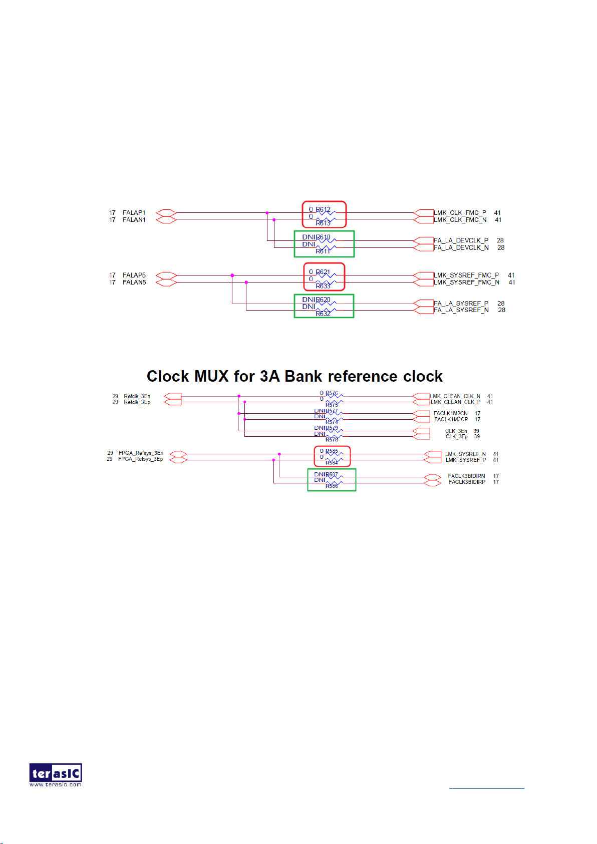
⚫ Remove the resistors on the R612 and R613 positions in the red box, then install 0 Ohm resistors
on the R610 and R611 positions in the green box, as shown in Figure 4-5.
In the default resistors setting, the TX_PCLK and SiI9136_RST_N signals are not controlled, there
will be no image outputting on the monitor. After modifying this group of resistors, there will be
image output.
⚫ Remove the resistors on the R621 and R633 positions in the red box, then install 0 Ohm resistors
on the R620 and R632 positions in the green box, as shown in Figure 4-5.
In the default resistors setting, the TX_BD4 and TX_BD10 signals are not controlled, the expected
black color of the output image will display blue. After modifying this group of resistors, the black
color of the output image will display normally.
Page 41
- 40 -
HDMI-FMC_User_Manual www.terasic.com
August 6, 2019
⚫ Remove the resistors on the R585 and R584 positions in the red box, then install 0 Ohm resistors on
the R587 and R586 positions in the green box, as shown in Figure 4-6.
In the default resistors setting, the RX_RD14 and RX_RD15 signals don’t input to FPGA, the red
color will be not normal. After modifying this group of resistors, the red color will display normally.
Figure 4-5 The resistors need to be reworked
Figure 4-6 The resistors need to be reworked
Figure 4-7 shows the resistors (that need to be reworked) positions on A10SoC Production board
PCB.
Page 42

- 41 -
HDMI-FMC_User_Manual www.terasic.com
August 6, 2019
Figure 4-7 The resistors positions on the PCB
2. Make sure Quartus 18.1 or later version has been installed on your PC.
3. Program the max5.pof code into A10SoC I/O MAX V as the steps below:
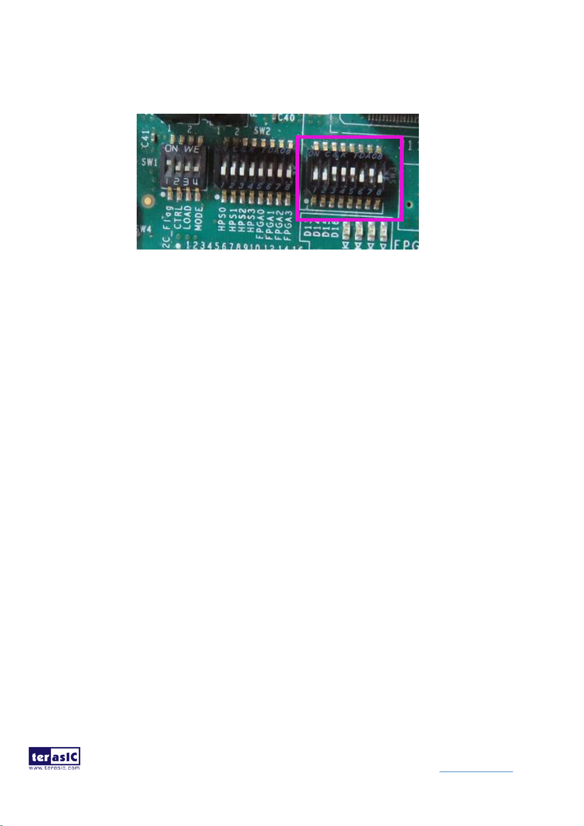
⚫ Set the switches of the SW3 as shown in the Figure 4-8 first.
Page 43

- 42 -
HDMI-FMC_User_Manual www.terasic.com
August 6, 2019
Figure 4-8 SW3 setting
⚫ Connect the PC with A10SoC USB-Blaster II connector via USB cable. Then power on the
A10SoC board, open the Quartus Programmer tool, click Auto Detect, see Figure 4-9.
Figure 4-9 Quartus Programmer windows
⚫ Select the max5.pof file (in the …\A10SoC_HDMI_FMC\demo_batch folder) into the
MAX V device, see Figure 4-10.
Page 44

- 43 -
HDMI-FMC_User_Manual www.terasic.com
August 6, 2019
Figure 4-10 Select the max5.pof file
⚫ Click Start button to program as shown in Figure 4-11.
Figure 4-11 Program the max5.pof
⚫ After programming successfully, power off the A10SoC board and set the switches of the
SW3 as shown in Figure 4-12.
Page 45
- 44 -
HDMI-FMC_User_Manual www.terasic.com
August 6, 2019
Figure 4-12 SW3 setting
4. Connect the FMC-HDMI daughter board to A10SoC board via FMCA connector and make sure
the screws on the HDMI-FMC card have been tightened firmly.
5. Connect the 4K HDMI monitor and the HDMI TX port with a HDMI cable, power on the
monitor and make sure the monitor is set to HDMI input mode.
6. Connect the 4K HDMI source device (such as HDMI video player) and HDMI RX port (HDMI
RX0 or HDMI RX1 port) on the FMC-HDMI board with a HDMI cable, power on the HDMI source
device and make sure its HDMI port is selected as the output.
7. Connect PC with A10SoC board USB-Blaster II port via a mini USB cable.
8. Power on A10SoC board.
9. Execute the batch file test.bat under the folder “…\ A10SoC_HDMI_FMC\demo_batch”.
Page 46

- 45 -
HDMI-FMC_User_Manual www.terasic.com
August 6, 2019
Chapter 5
Appendix
5-1 Revision History
Version
Date
Change Log
V1.0
Initial Version
V1.1
2017/06/03
Add A10SoC Setup Figure
V1.2
2017/11/30
Modify Figure 2-3 and Figure 3-1
V1.3
2018/3/7
Add Register Tables and Demo Setup Steps
V1.4
2018/7/3
Modify steps number from 10,11,12 to 8,9,10 in Page 43,
44 and marked as red color
V1.5
2019/6/28
Modify section 4-1, add new operation step 2 for TR5
demo
V1.6
2019/08/05
Add HAN+HDMI-FMC demo, change the A10SoC ES
board to A10SoC Production board
5-2 Copyright Statement
Copyright © 2017 Terasic Inc. All rights reserved.
 Loading...