

Page 1
Page 2
DE1-SoC-MTL2 User Manual
1
www.terasic.com
December 18, 2014
CONTENTS
CHAPTER 1
INTRODUCTION
............................................................................................................. 3
1.1 Key Features ............................................................................................................................................... 4
1.2 About the Kit .............................................................................................................................................. 6
1.3 Power On Test ............................................................................................................................................ 7
1.4 System CD and Linux BSP ........................................................................................................................ 8
1.5 Getting Help ............................................................................................................................................... 8
CHAPTER 2
ARCHITECTURE
............................................................................................................ 9
2.1 Layout and Components ............................................................................................................................. 9
2.2 Block Diagram .......................................................................................................................................... 10
2.3 ITG Adapter .............................................................................................................................................. 11
CHAPTER 3
USING DE1-SOC-MTL2
................................................................................................ 13
3.1 Using FPGA ............................................................................................................................................. 13
3.2 Pin Definition of 2x20 GPIO Connector .................................................................................................. 13
3.3 Using LCD................................................................................................................................................ 15
3.4 Using Terasic Multi-touch IP .................................................................................................................... 17
CHAPTER 4
LINUX BSP
................................................................................................................... 20
4.1 Board Support Package ............................................................................................................................ 20
4.2 Linux Image Files ..................................................................................................................................... 21
4.3 Quarts Project ........................................................................................................................................... 21
4.4 QT Libraries ............................................................................................................................................. 22
CHAPTER 5
PAINTER DEMONSTRATION
....................................................................................... 23
5.1 Operation Description .............................................................................................................................. 23
5.2 System Description ................................................................................................................................... 25
5.3 Demonstration Setup ................................................................................................................................ 25
5.4 Demonstration Source Code ..................................................................................................................... 26
Page 3

DE1-SoC-MTL2 User Manual
2
www.terasic.com
December 18, 2014
CHAPTER 6
APPENDIX
.................................................................................................................... 27
6.1 Revision History ....................................................................................................................................... 27
6.2 Copyright Statement ................................................................................................................................. 27
Page 4
DE1-SoC-MTL2 User Manual
3
www.terasic.com
December 18, 2014
Chapter 1
Introduction
The DE1-SoC-MTL2 Development Kit is a comprehensive design environment with everything
embedded developers need to create processing-based systems. The DE1-SoC-MTL2 delivers an
integrated platform including hardware, design tools, and reference designs for developing
embedded software and hardware platforms in a wide range of applications. The fully integrated kit
allows developers to rapidly customize their processor and IP to best suit their specific application.
The DE1-SoC-MTL2 features a DE1-SoC development board targeting Altera Cyclone® V SoC
FPGA, as well as a 5-Point capacitive LCD multimedia color touch panel which natively supports
five points multi-touch and gestures.
The all-in-one embedded solution offered on the DE1-SoC-MTL2, in combination of a LCD touch
panel and digital image module, provides embedded developers the ideal platform for multimedia
applications with unparallel processing performance. Developers can benefit from the use of
FPGA-based embedded processing system such as mitigating design risk and obsolescence, design
reuse, lowering bill of material (BOM) costs by integrating powerful graphics engines within the
FPGA.
For SoC reference design in Linux for touch-screen display, please refer to the “Programming
Guide for Touch-Screen Display” document in the System CD of DE1-SoC-MTL2.
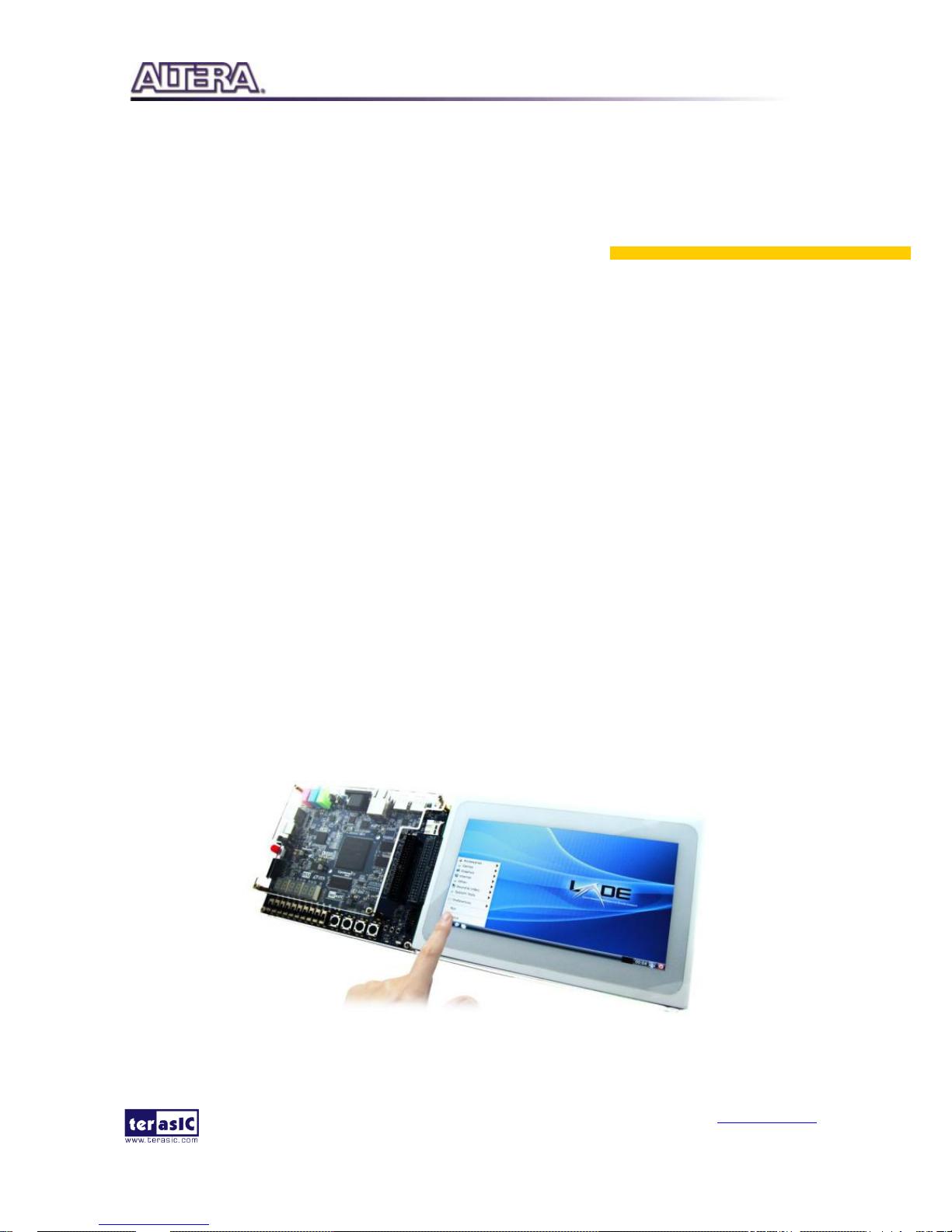
Figure 1-1 shows a photo of DE1-SoC-MTL2.
Figure 1-1 The DE1-SoC-MTL2 platform
Page 5
DE1-SoC-MTL2 User Manual
4
www.terasic.com
December 18, 2014
11..1
1
KKeeyy FFeeaattuurreess
The key features of this kit are listed below:
Cyclone V SE SoC—5CSEMA5F31C6N
o Dual-core ARM Cortex-A9 (HPS)
o 85K programmable logic elements
o 4,450 Kbits embedded memory
o 6 fractional PLLs
o 2 hard memory controllers
Configuration Sources
o Quad serial configuration device – EPCS128 for the FPGA
o On-board USB Blaster II (normal type B USB connector)
Memory Devices
o 64MB (32Mx16) SDRAM for the FPGA
o 1GB (2x256MBx16) DDR3 SDRAM for the HPS
o microSD card socket for the HPS
Peripherals
o Two port USB 2.0 Host (ULPI interface with USB type A connector)
o UART to USB (USB Mini B connector)
o 10/100/1000 Ethernet
o PS/2 mouse/keyboard
o IR emitter/receiver
o I2C multiplexer
Connectors
o Two 40-pin expansion headers
o One 10-pin ADC input header
o One LTC connector (one Serial Peripheral Interface (SPI) master ,one I2C bus, and one
GPIO interface)
Page 6

DE1-SoC-MTL2 User Manual
5
www.terasic.com
December 18, 2014
Display
o 24-bit VGA DAC
Audio
o 24-bit CODEC, line-in, line-out, and microphone-in jacks
Video Input
o TV decoder (NTSC/PAL/SECAM) and Video-in connector
ADC
o Fast throughput rate: 1 MSPS
o Channel number: 8
o Resolution: 12-bit
o Analog input range : 0 ~ 2.5 V or 0 ~ 5V by selecting the RANGE bit in the control register
Switches, Buttons and LEDs
o 5 user keys (4 for the FPGA and 1 for the HPS)
o 10 user switches for the FPGA
o 11 user LEDs (10 for the FPGA and 1 for the HPS)
o 2 HPS reset buttons (HPS_RESET_n and HPS_WARM_RST_n)
o Six 7-segment displays
Sensor
o G-sensor for the HPS
Power
o 12V DC input
Capacitive LCD Touch Screen
o Equipped with an 7-inch Amorphous-TFT-LCD (Thin Film Transistor Liquid
Crystal Display) module
o 800x600x3(RGB) Resolution
Page 7
DE1-SoC-MTL2 User Manual
6
www.terasic.com
December 18, 2014
o 24-bit parallel RGB interface
o Supports 5-point touch
Table 1-1 shows the general physical specifications of the touch-screen (Note*).
Table 1-1 General physical specifications of the LCD
Item
Specification
Unit
LCD size
7-inch (Diagonal)
-
Resolution
800 x3(RGB) x 480
dot
Display mode
Normally White, Transmissive
-
Dot pitch
0.0642(W) x0.1790 (H)
mm
Active area
154.08 (W) x 85.92 (H)
mm
Module size
179.4(W) x 117.4(H) x 7.58(D)
mm
Surface treatment
Anti-Glare
-
Color arrangement
RGB-stripe
-
Interface
Digital
-
Backlight power
consumption
1.674(Typ.)
W
Panel power
consumption
0.22(Typ.)
W
11..2
2
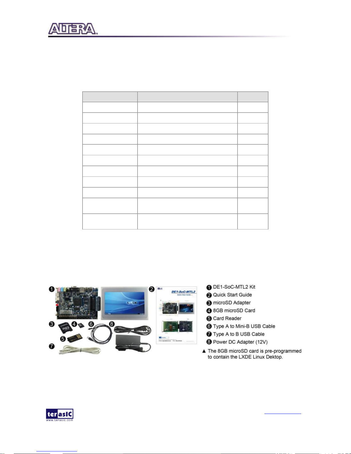
AAbboouutt tthhee KKiitt
The kit includes everything users need to run the demonstrations and develop custom designs, as shown
in Figure 1-2.
Figure 1-2 Contents of DE1-SoC-MTL2 kit package
Page 8
DE1-SoC-MTL2 User Manual
7
www.terasic.com
December 18, 2014
11..3
3
PPoowweerr OOnn TTeesstt
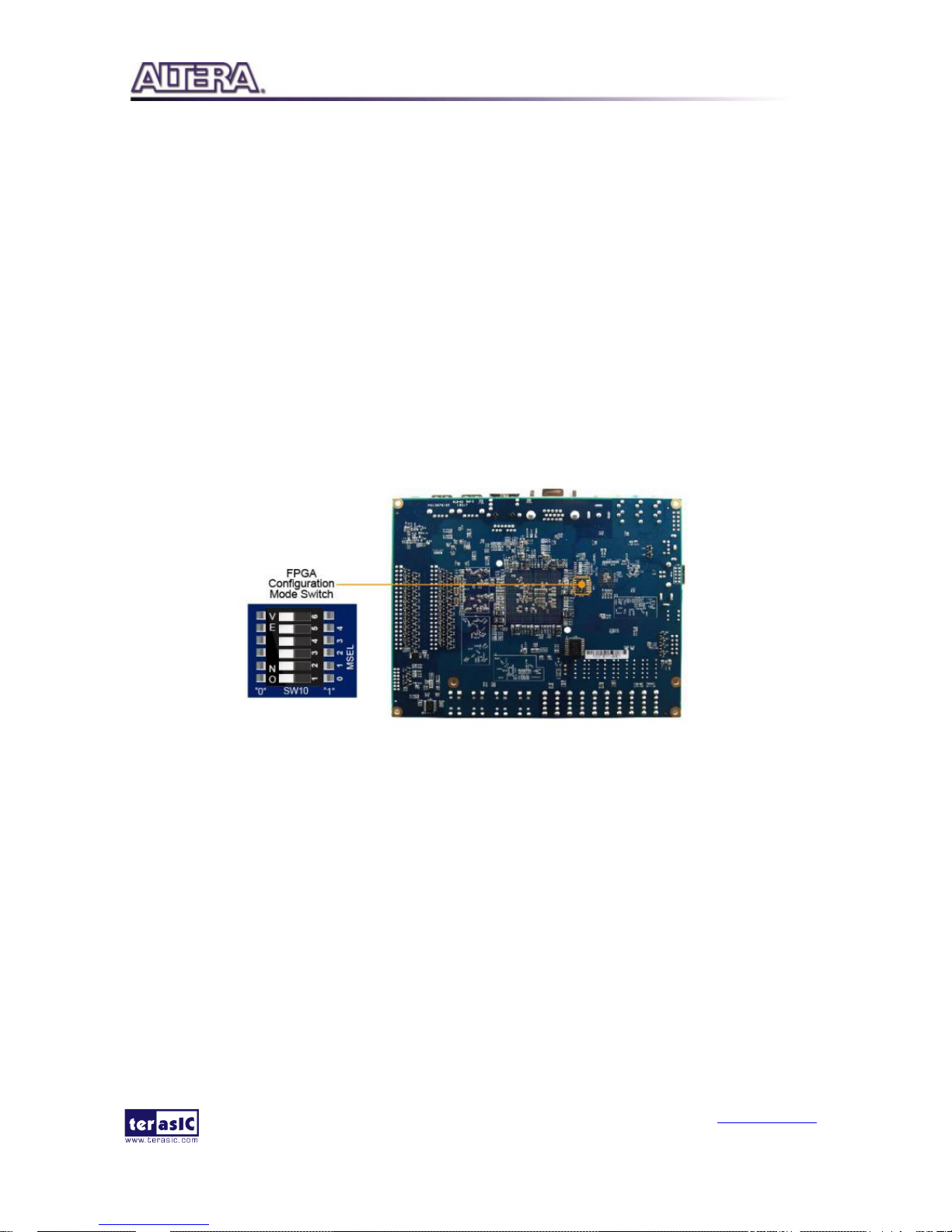
The 8GB microSD card included in the kit is pre-programmed with LXDE Linux desktop. Users
can perform a power on test from the microSD card. The procedures to perform the power on test
are:
1. Please make sure the microSD card is inserted to the microSD card socket (J11) onboard.
2. Set MSEL[4:0] = 00000, as shown in Figure 1-3.
3. Plug in a USB keyboard to the USB host on the DE1-SoC board.
4. Plug in the 12V DC power supply to the DE1-SoC board.
5. Power on the DE1-SoC board.
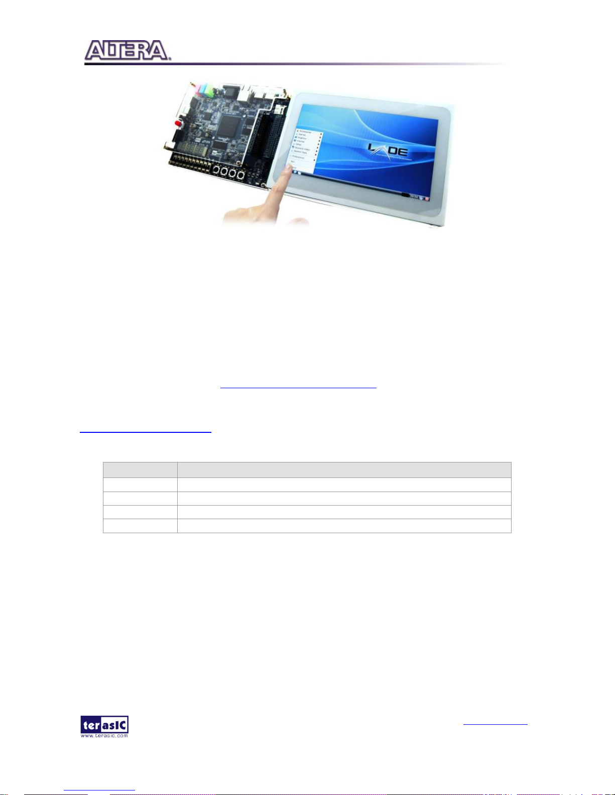
6. The LXDE Desktop will appear on the LCD display.
7. Use the touch-screen to select the system menu, as shown in Figure 1-4.
Figure 1-3 MSEL[4:0] = 00000
Page 9
DE1-SoC-MTL2 User Manual
8
www.terasic.com
December 18, 2014
Figure 1-4 LXDE desktop on DE1-SoC-MTL2 platform
11..4
4
SSyysstteemm CCDD aanndd LLiinnuuxx BBSSPP
The DE1-SoC-MTL2 System CD contains the touch-screen documentations and supporting
materials, including the user manual, reference designs, and device datasheets. Users can download
the System CD form the link: http://cd-de1-soc-mtl2.terasic.com. This site also provides the Linux
image files for creating a bootable microSD card. Table 1-1 shows the contents of DE1-SoC-MTL2
System CD. For the system CD of DE1-SoC mainboard, users can download it from the link:
http://cd-de1-soc.terasic.com.
Table 1-1 Contents of DE1-SoC-MTL2 System CD
Folder Name
Description
Datasheet
Specifications for major components on the touch-screen display module
Demonstrations
FPGA and SoC design examples
Manual
Including user manual and software programming guide
Schematic
Schematic of the touch-screen display module
11..5
5
GGeettttiinngg HHeellpp
Here is the contact information should you encounter any problem:
Terasic Technologies
Tel: +886-3-575-0880
Email: support@terasic.com
Page 10

DE1-SoC-MTL2 User Manual
9
www.terasic.com
December 18, 2014
Chapter 2
Architecture
This chapter provides information regarding the features and architecture of DE1-SoC-MTL2. The
kit is composed of DE1-SoC mainboard and MTL (Multi-Touch LCD) module. The MTL module is
connected to a 2x20 GPIO expansion header on DE1-SoC board through an ITG (IDE to GPIO)
adaptor. For more information about the DE1-SoC mainboard, please refer to the user manual in
DE1-SoC System CD, which can be download from the link: http://cd-de1-soc.terasic.com.
22..1
1
LLaayyoouutt aanndd CCoommppoonneennttss
Figure 2-1 and Figure 2-2 show photos of DE1-SoC-MTL2. It depicts the layout of the board and
indicates the locations of connectors and key components.
Figure 2-1 DE1-SoC-MTL2 (top view)
Page 11

DE1-SoC-MTL2 User Manual
10
www.terasic.com
December 18, 2014
Figure 2-2 DE1-SoC-MTL2 (bottom view)
22..2
2
BBlloocckk DDiiaaggrraamm
Figure 2-3 shows the block diagram of MTL2 module. The IDE connector bridges all the wires
from the peripherals to the FPGA through an ITG adapter.
Figure 2-3 Block diagram of MTL2
Page 12

DE1-SoC-MTL2 User Manual
11
www.terasic.com
December 18, 2014
Figure 2-4 illustrates the connection of MTL2 to Terasic FPGA board.
Figure 2-4 Connection Diagram of MTL2 Kit with Terasic FPGA boards
22..3
3
IITTGG AAddaapptteerr
The IDE to GPIO (ITG) adapter is designed to remap IDE pins to GPIO pins.
CCoommppoonneenntt aanndd LLaayyoouut
t
Figure 2-5 and
Figure 2-6 show the top and bottom view of ITG adapter, respectively.
The J1 connector is used to connect the FPGA board. The J2 connector is used to interface with the
IDE cable.
Page 13

DE1-SoC-MTL2 User Manual
12
www.terasic.com
December 18, 2014
Figure 2-5 ITG adapter (top view)
Figure 2-6 ITG adapter (bottom view)
Page 14

DE1-SoC-MTL2 User Manual
13
www.terasic.com
December 18, 2014
Chapter 3
Using DE1-SoC-MTL2
This chapter provides information on how to control the Multi-touch LCD Module Second Edition
(MTL2) hardware, which includes the definition of 2x20 GPIO interface, LCD control, and
multi-touch control signals.
33..1
1
UUssiinngg FFPPGGAA
The DE1-SoC-MTL2 is composed of DE1-SoC SoC development board and 7" touch panel
daughter card. The DE1-SoC SoC development board with the FPGA device is considered as the
main part. The DE1-SoC user manual and CD are available at: http://cd-de1-soc.terasic.com
33..2
2
PPiinn DDeeffiinniittiioonn ooff 22xx2200 GGPPIIOO CCoonnnneeccttoorr
The 2x20 GPIO female connector directly connects to the 2x20 GPIO male connector on the Terasic
FPGA development boards. Figure 3-1 shows the signal names of the 2x20 GPIO from the ITG
adapter.
Page 15

DE1-SoC-MTL2 User Manual
14
www.terasic.com
December 18, 2014
Figure 3-1 Signals of 2x20 GPIO connector
Table 3-1 shows the recommended pin assignments for the 2x20 GPIO pins in Quartus II.
Table 3-1 Recommended Pin Assignments of 2x20 GPIO in Quartus II
Pin Numbers
Pin Name
Direction
IO Standard
1
- - -
2
MTL_DCLK
Output
3.3-V LVTTL
3
- - -
4
MTL_R[0]
Output
3.3-V LVTTL
5
MTL_R[1]
Output
3.3-V LVTTL
6
MTL_R[2]
Output
3.3-V LVTTL
7
MTL_R[3]
Output
3.3-V LVTTL
8
MTL_R[4]
Output
3.3-V LVTTL
9
MTL_R[5]
Output
3.3-V LVTTL
10
MTL_R[6]
Output
3.3-V LVTTL
11 - - - 12 - -
-
13
MTL_R[7]
Output
3.3-V LVTTL
14
MTL_G[0]
Output
3.3-V LVTTL
15
MTL_G[1]
Output
3.3-V LVTTL
16
MTL_G[2]
Output
3.3-V LVTTL
17
MTL_G[3]
Output
3.3-V LVTTL
Page 16

DE1-SoC-MTL2 User Manual
15
www.terasic.com
December 18, 2014
18
MTL_G[4]
Output
3.3-V LVTTL
19 - - - 20 - - - 21
MTL_G[5]
Output
3.3-V LVTTL
22
MTL_G[6]
Output
3.3-V LVTTL
23
MTL_B[0]
Output
3.3-V LVTTL
24
MTL_G[7]
Output
3.3-V LVTTL
25
MTL_B[1]
Output
3.3-V LVTTL
26
MTL_B[2]
Output
3.3-V LVTTL
27
MTL_B[3]
Output
3.3-V LVTTL
28
MTL_B[4]
Output
3.3-V LVTTL
29 - -
-
30 - -
-
31
MTL_B[5]
Output
3.3-V LVTTL
32
MTL_B[6]
Output
3.3-V LVTTL
33
MTL_B[7]
Output
3.3-V LVTTL
34 - - - 35
MTL_HSD
Output
3.3-V LVTTL
36
MTL_VSD
Output
3.3-V LVTTL
37
MTL_TOUCH_I2C_SCL
Output
3.3-V LVTTL
38
MTL_TOUCH_I2C_SDA
Inout
3.3-V LVTTL
39
MTL_TOUCH_INT_n
Input
3.3-V LVTTL
40 - -
-
33..3
3
UUssiinngg LLCCDD
The LCD features 800x480 pixel resolution and runs at 33 MHz pixel rate. There is no
configuration required to drive the LCD. The timing specification is defined as in the Table 3-2,
Table 3-3, Figure 3-2 and Figure 3-3.
Table 3-2 LCD Horizontal Timing Specifications
Item
Symbol
Typical Value
Unit
Min.
Typ.
Max.
Horizontal Display Area
thd - 800
-
DCLK
DCLK Frequency
fclk
26.4
33.3
46.8
MHz
One Horizontal Line
th
862
1056
1200
DCLK
HS pulse width
thpw 1
40
DCLK
HS Blanking
thb
46
46
46
DCLK
HS Front Porch
thfp
16
210
354
DCLK
Page 17

DE1-SoC-MTL2 User Manual
16
www.terasic.com
December 18, 2014
Table 3-3 LCD Vertical Timing Specifications
Item
Symbol
Typical Value
Unit
Min.
Typ.
Max.
Vertical Display Area
tvd - 480
-
TH
VS period time
tv
510
525
650
TH
VS pulse width
tvpw 1 -
20
TH
VS Blanking
tvb
23
23
23
TH
HS Front Porch
tvfp 7 22
147
TH
Figure 3-2 Horizontal input timing waveform
Figure 3-3 Vertical input timing waveform
Page 18

DE1-SoC-MTL2 User Manual
17
www.terasic.com
December 18, 2014
33..4
4
UUssiinngg TTeerraassiicc MMuullttii--ttoouucchh IIPP
Terasic Multi-touch IP is provided for developers to retrieve user inputs, including multi-touch
gestures and single-touch. The file name of this IP is i2c_touch_config.v, which is located in
System CD \IP folder.
The IP decodes I2C information and outputs coordinates and gesture information. The inputs and
outputs of this IP module is shown below
The purpose of signals for this IP is described in Table 3-4. The IP requires a 50 MHz signal as a
reference clock to the iCLK pin and system reset signal to the iRSTN. INT_n, The signals of
I2C_SCLK, and I2C_SDAT pins should be connected to the MTL2_TOUCH_INT_n,
MTL2_TOUCH_I2C_SCL, and MTL2_TOUCH_I2C_SDA signals in the 2x20 GPIO header,
respectively.
When touch activity occurs, the control application should check whether the value of
oREG_GESTURE matches a pre-defined gesture ID defined in Table 3-4 and the relative X/Y
coordinates can be derived from oREG_X and oREG_Y. Figure 3-1 shows the signaltap II
waveform of the IP. When the oREADY rises, it indicates touch activity, and the associated
information can be collected from the oREG_X1~ oREG_X5, oREG_Y1~ oREG_Y5,
oREG_TOUCH_COUNT, and oREG_GESTURE pins.
Page 19

DE1-SoC-MTL2 User Manual
18
www.terasic.com
December 18, 2014
Figure 3-4 Signaltap II Waveform for Multi-Touch IP
Table 3-4 Definition of Terasic Multi-touch IP Signals
Pin Name
Direction
Description
iCLK
Input
Connect to 50MHz clock
iRSTN
Input
Connect to system reset signal
INT_n
Input
Connect to interrupt pin of touch IC
oREADY
Output
Triggered when the data of following six
outputs are valid
oREG_X1
Output
10-bit X coordinate of first touch point
oREG_Y1
Output
9-bit Y coordinate of first touch point
oREG_X2
Output
10-bit X coordinate of second touch point
oREG_Y2
Output
9-bit Y coordinate of second touch point
oREG_X3
Output
10-bit X coordinate of first touch point
oREG_Y3
Output
9-bit Y coordinate of second touch point
oREG_X4
Output
10-bit X coordinate of first touch point
oREG_Y4
Output
9-bit Y coordinate of second touch point
oREG_X5
Output
10-bit X coordinate of first touch point
oREG_Y5
Output
9-bit Y coordinate of second touch point
oREG_TOUCH_COUNT
Output
2-bit touch count. Valid value is 0, 1, or 2.
oREG_GESTURE
Output
8-bit gesture ID (See Table 3-5)
I2C_SCLK
Output
Connect to I2C clock pin of touch IC
I2C_SDAT
Inout
Connect to I2C data pin of touch IC
The gestures and IDs supported are shown in Table 3-5.
Page 20

DE1-SoC-MTL2 User Manual
19
www.terasic.com
December 18, 2014
Table 3-5 Gestures and Its IDs
Gesture
ID (hex)
Move Up
0x10
Move Left
0x14
Move Down
0x18
Move Right
0x1C
Zoom In
0x48
Zoom Out
0x49
No Gesture
0x00
Note: The Terasic IP Multi-touch IP can also be found under the \IP folder in the system CD, as well
as the reference designs.
Page 21

DE1-SoC-MTL2 User Manual
20
www.terasic.com
December 18, 2014
Chapter 4
Linux BSP
This chapter describes how to use the Linux BSP (Board Support Package) provide by Terasic.
Users can develop touch-screen GUI program easily with the BPS including QT 5.3.1 library.
44..1
1
BBooaarrdd SSuuppppoorrtt PPaacckkaaggee
Figure 4-1 shows the block diagram of Linux BSP for DE1-SoC-MTL2 kit. The BPS incudes three
major parts:
Linux image files
Quartus project
QT library with touch-screen function included
The Linux image files are implemented on HPS/ARM and the Quartus project is implemented on
FPGA/Qsys. The Linux image files include the pre-built Linux system. Users can create a Linux
bootable microSD card with the image files. The Quartus project includes the controller for VGA
display and the touch-screen controller for touch-screen panel.
The BSP includes not only precompiled QT library and touch-screen library in the Linux image
files, but also the document that show how to cross-compile these libraries, as well as to develop
touch-screen GUI program based on these libraries.
Figure 4-1 Block diagram of Linux BSP for DE1-SoC-MTL2 kit
Page 22

DE1-SoC-MTL2 User Manual
21
www.terasic.com
December 18, 2014
44..2
2
LLiinnuuxx IImmaaggee FFiilleess
LXDE desktop Linux image file is provided for DE1-SoC-MTL2. It is available from the link:
http://cd-de1-soc-mtl2.terasic.com. Developers can use a tool named Win32 Disk Imager to write
the image file into a microSD card. For details about how to create a bootable microSD card or
booting Linux from the DE1-SoC board, please refer to the chapter 5 of
DE1-SoC_Getting_Started_Guide.pdf, which is included in the DE1-SoC System CD, which is
available from the link: http://cd-de1-soc.terasic.com.
Figure 4-2 shows a screenshot of LXDE desktop after booting. The LXDE desktop is displayed on
the LCD touch panel. This image file also includes the QT library and touch-screen library. To
perform these demos, users need to double click the icons of the demos on desktop.
Figure 4-2 Screenshot of LXDE desktop
44..3
3
QQuuaarrttss PPrroojjeecctt
The Quartus project is designed based on Altera Qsys tool. There are three major parts:
VGA display
Touch-screen
HPS component
The VGA display part is designed to display the Linux console or desktop on the LCD touch panel.
Altera Video and Image Processing (VIP) suite is used to implement this function. The Linux frame
Page 23

DE1-SoC-MTL2 User Manual
22
www.terasic.com
December 18, 2014
buffer driver fills up the DDR3 with data to be displayed, and the VIP frame-reader component
reads the data from the DDR3 in a DMA manner. The video data is streamed into the VIP Clocked
Video Output component. Finally, the VIP Clocked Video Output component drives the VGA DAC
chip to display the video data.
An I2C master controller in Qsys is used to communicate with the touch-screen panel. The
component interfaces with the touch-screen panel through I2C protocol.
The HPS communicate with the FPGA through AXI bridge. The components in FPGA are mapped
into user memory of the linux system through memory-mapped interface. Then the user software
can access the IPs in FPGA portion. The Quartus project is located under the folder
“Demonstrations/SoC_FPGA/MTL2_HPS” in the DE1-SoC-MTL2 system CD.
44..4
4
QQTT LLiibbrraarriieess
Users can develop touch-screen GUI program based on the QT library. For more information,
please refer to the document “Software Development Guide for touch-screen display.pdf”
included in the DE1-SoC-MTL2 system CD. The precompiled libraries can be found from the
folder “Demonstrations/SoC_FPGA/Libraries” in the DE1-SoC-MTL2 system CD.
Page 24

DE1-SoC-MTL2 User Manual
23
www.terasic.com
December 18, 2014
Chapter 5
Painter Demonstration
This chapter shows how to implement a painter demo on the Multi-touch LCD module based on
Altera Qsys tool and the Video and Image Processing (VIP) suite. It demonstrates how to use
multi-touch gestures and resolution. The GUI of this demonstration is controlled by the program in
Nios II.
55..1
1
OOppeerraattiioonn DDeessccrriippttiioonn
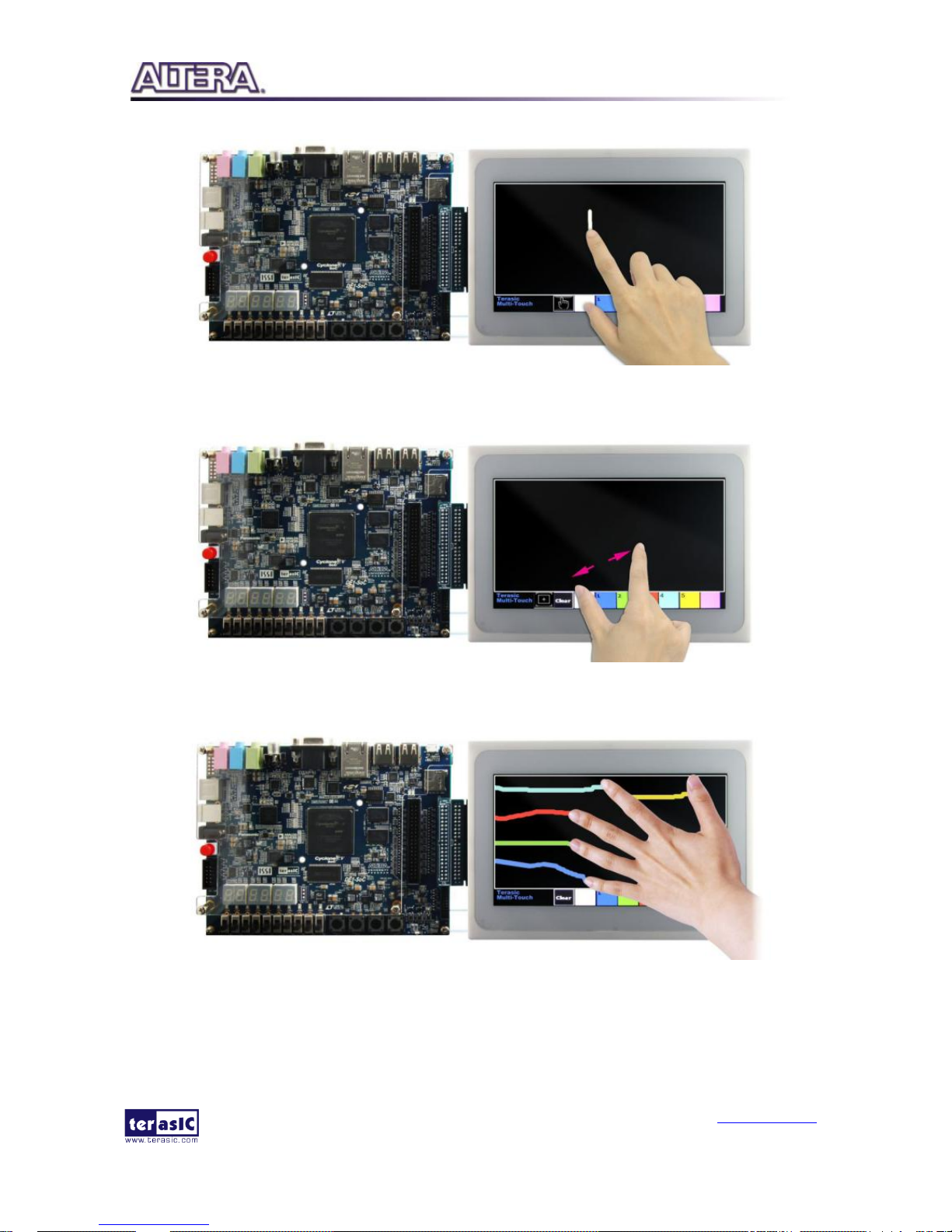
Figure 5-1 shows the Graphical User Interface (GUI) of Painter demo. The GUI is classified into
four separate areas: Painting Area, Gesture Indicator, Clear Button, and Color Palette. Users can
select a color from the color palette and start painting in the paint area. If a gesture is detected, the
associated gesture symbol will be shown in the gesture area. To clear the painting area, click the
“Clear” button.
Figure 5-1 GUI of Painter Demo
Page 25
DE1-SoC-MTL2 User Manual
24
www.terasic.com
December 18, 2014
Figure 5-2 shows the single-finger painting of canvas area.
Figure 5-2 Single-finger painting
Figure 5-3 shows the zoom-in gesture.
Figure 5-3 Zoom-in gesture
Figure 5-4 5-Point painting of canvas area.
Figure 5-4 5-Point painting
Page 26

DE1-SoC-MTL2 User Manual
25
www.terasic.com
December 18, 2014
55..2
2
SSyysstteemm DDeessccrriippttiioonn
For LCD display processing, the reference design is developed based on Altera’s Video and Image
Processing (VIP) suite. The Frame Reader VIP is used for reading data to be displayed from the
associated video memory, and the VIP Video Out is used to display the video data. The data is
drawn by the Nios II processor according to user input.
For multi-touch processing, When touch activity occurs, a I2C Controller IP is used to retrieve
serial data from the I2C interface, the associated touch information including multi-touch gestures
and 5 Point touch coordinates can be calculated through the data in NIOS II. Note: the license for
this IP must be installed before compiling the Quartus II project including this encrypted
component.
Figure 5-5 shows the system generic block diagram of painter demonstration.
Figure 5-5 System block diagram of painter demonstration
55..3
3
DDeemmoonnssttrraattiioonn SSeettuupp
Please follow the procedures below to setup the demonstration:
Page 27

DE1-SoC-MTL2 User Manual
26
www.terasic.com
December 18, 2014
1. Connect the DE1-SoC-MTL2 USB-Blaster II USB port to the PC USB Port with a USB
Cable.
2. Power on the DE1-SoC-MTL2.
3. Please make sure Quartus II v14.0 has been installed on the host PC.
4. Copy the folder \Demonstrations\FPGA\DE1_SoC_MTL2_PAINTER\demo_batch.
5. Execute “DE1_SoC_MTL2_PAINTER.bat”.
6. The painter GUI will show up on the LCD panel.
5.4
DDeemmoonnssttrraattiioonn SSoouurrccee CCoodde
e
The locations of this demonstration source code are shown in Table 5-1. Note: The project is built
under Quartus II v14.0. Both Altera VIP license is required to rebuild the project.
Table 5-1 Locations of Painter Demonstration Source Code
Project
Location
Quartus II
Demonstrations\FPGA\DE1_SoC_MTL_PAINTER
Nios II
Demonstrations\FPGA\DE1_SoC_MTL_PAINTER\software
Page 28

DE1-SoC-MTL2 User Manual
27
www.terasic.com
December 18, 2014
Chapter 6
Appendix
66..1
1
RReevviissiioonn HHiissttoorryy
Version
Change Log
V1.0
Initial Version (Preliminary)
66..2
2
CCooppyyrriigghhtt SSttaatteemmeenntt
Copyright © 2014 Terasic Technologies. All rights reserved.
 Loading...