

Page 1
DE10-Standard
User Manual
1
www.terasic.com
January 19, 2017
Page 2

DE10-Standard
User Manual
1
www.terasic.com
January 19, 2017
CONTENTS
Chapter 1 DE10-Standard Development Kit .................................................. 4
1.1 Package Contents ....................................................................................................................... 4
1.2 DE10-Standard System CD ........................................................................................................ 5
1.3 Getting Help ............................................................................................................................... 5
Chapter 2 Introduction of the DE10-Standard Board ..................................... 7
2.1 Layout and Components ............................................................................................................. 7
2.2 Block Diagram of the DE10-Standard Board ............................................................................. 9
Chapter 3 Using the DE10-Standard Board ................................................ 13
3.1 Settings of FPGA Configuration Mode .................................................................................... 13
3.2 Configuration of Cyclone V SoC FPGA on DE10-Standard .................................................... 14
3.3 Board Status Elements.............................................................................................................. 20
3.4 Board Reset Elements .............................................................................................................. 21
3.5 Clock Circuitry ......................................................................................................................... 22
3.6 Peripherals Connected to the FPGA ......................................................................................... 23
3.6.1 User Push-buttons, Switches and LEDs ................................................................ 23
3.6.2 7-segment Displays ............................................................................................... 27
3.6.3 2x20 GPIO Expansion Header .............................................................................. 28
3.6.4 HSMC connector ................................................................................................... 30
3.6.5 24-bit Audio CODEC ............................................................................................ 34
3.6.6 I2C Multiplexer ..................................................................................................... 34
3.6.7 VGA Output ........................................................................................................... 35
3.6.8 TV Decoder ........................................................................................................... 38
3.6.9 IR Receiver ............................................................................................................ 40
3.6.10 IR Emitter LED ..................................................................................................... 40
3.6.11 SDRAM Memory .................................................................................................. 41
Page 3

DE10-Standard
User Manual
2
www.terasic.com
January 19, 2017
3.6.12 PS/2 Serial Port ...................................................................................................... 43
3.6.13 A/D Converter and 2x5 Header ............................................................................. 44
3.7 Peripherals Connected to Hard Processor System (HPS)......................................................... 46
3.7.1 User Push-buttons and LEDs ................................................................................. 46
3.7.2 Gigabit Ethernet ..................................................................................................... 46
3.7.3 UART to USB ........................................................................................................ 48
3.7.4 DDR3 Memory ...................................................................................................... 49
3.7.5 Micro SD Card Socket ........................................................................................... 51
3.7.6 2-port USB Host .................................................................................................... 51
3.7.7 Accelerometer (G-sensor) ...................................................................................... 52
3.7.8 LTC Connector ...................................................................................................... 53
3.7.9 128x64 Dots LCD .................................................................................................. 54
Chapter 4 DE10-Standard System Builder .................................................. 56
4.1 Introduction .............................................................................................................................. 56
4.2 Design Flow ............................................................................................................................. 56
4.3 Using DE10-Standard System Builder ..................................................................................... 57
Chapter 5 Examples For FPGA .................................................................. 63
5.1 DE10-Standard Factory Configuration..................................................................................... 63
5.2 Audio Recording and Playing .................................................................................................. 64
5.3 Karaoke Machine ..................................................................................................................... 66
5.4 SDRAM Test in Nios II ............................................................................................................ 68
5.5 SDRAM Test in Verilog ........................................................................................................... 71
5.6 TV Box Demonstration ............................................................................................................ 73
5.7 PS/2 Mouse Demonstration ...................................................................................................... 75
5.8 IR Emitter LED and Receiver Demonstration ......................................................................... 78
5.9 ADC Reading ........................................................................................................................... 83
Chapter 6 Examples for HPS SoC ................................................................ 88
6.1 Hello Program .......................................................................................................................... 88
6.2 Users LED and KEY ................................................................................................................ 90
Page 4

DE10-Standard
User Manual
3
www.terasic.com
January 19, 2017
6.3 I2C Interfaced G-sensor ........................................................................................................... 96
6.4 I2C MUX Test .......................................................................................................................... 98
6.5 SPI Interfaced Graphic LCD .................................................................................................. 101
Chapter 7 Examples for using both HPS SoC and FGPA ............................ 105
7.1 Required Background ............................................................................................................. 105
7.2 System Requirements ............................................................................................................. 106
7.3 AXI bridges in Intel SoC FPGA ............................................................................................. 106
7.4 GHRD Project ........................................................................................................................ 107
7.5 Compile and Programming .................................................................................................... 109
7.6 Develop the C Code ............................................................................................................... 110
Chapter 8 Programming the EPCS Device ................................................. 116
8.1 Before Programming Begins .................................................................................................. 116
8.2 Convert .SOF File to .JIC File ................................................................................................ 116
8.3 Write JIC File into the EPCS Device ..................................................................................... 121
8.4 Erase the EPCS Device .......................................................................................................... 123
Chapter 9 Appendix ................................................................................... 125
9.1 Revision History ..................................................................................................................... 125
9.2 Copyright Statement ............................................................................................................... 125
Page 5
DE10-Standard
User Manual
4
www.terasic.com
January 19, 2017
Chapter 1
DE10-Standard
Development Kit
The DE10-Standard Development Kit presents a robust hardware design platform built around the
Altera System-on-Chip (SoC) FPGA, which combines the latest dual-core Cortex-A9 embedded
cores with industry-leading programmable logic for ultimate design flexibility. Users can now
leverage the power of tremendous re-configurability paired with a high-performance, low-power
processor system. Altera’s SoC integrates an ARM-based hard processor system (HPS) consisting of
processor, peripherals and memory interfaces tied seamlessly with the FPGA fabric using a
high-bandwidth interconnect backbone. The DE10-Standard development board is equipped with
high-speed DDR3 memory, video and audio capabilities, Ethernet networking, and much more that
promise many exciting applications.
The DE10-Standard Development Kit contains all the tools needed to use the board in conjunction
with a computer that runs the Microsoft Windows XP or later.
11..1
1
PPaacckkaaggee CCoonntteennttss
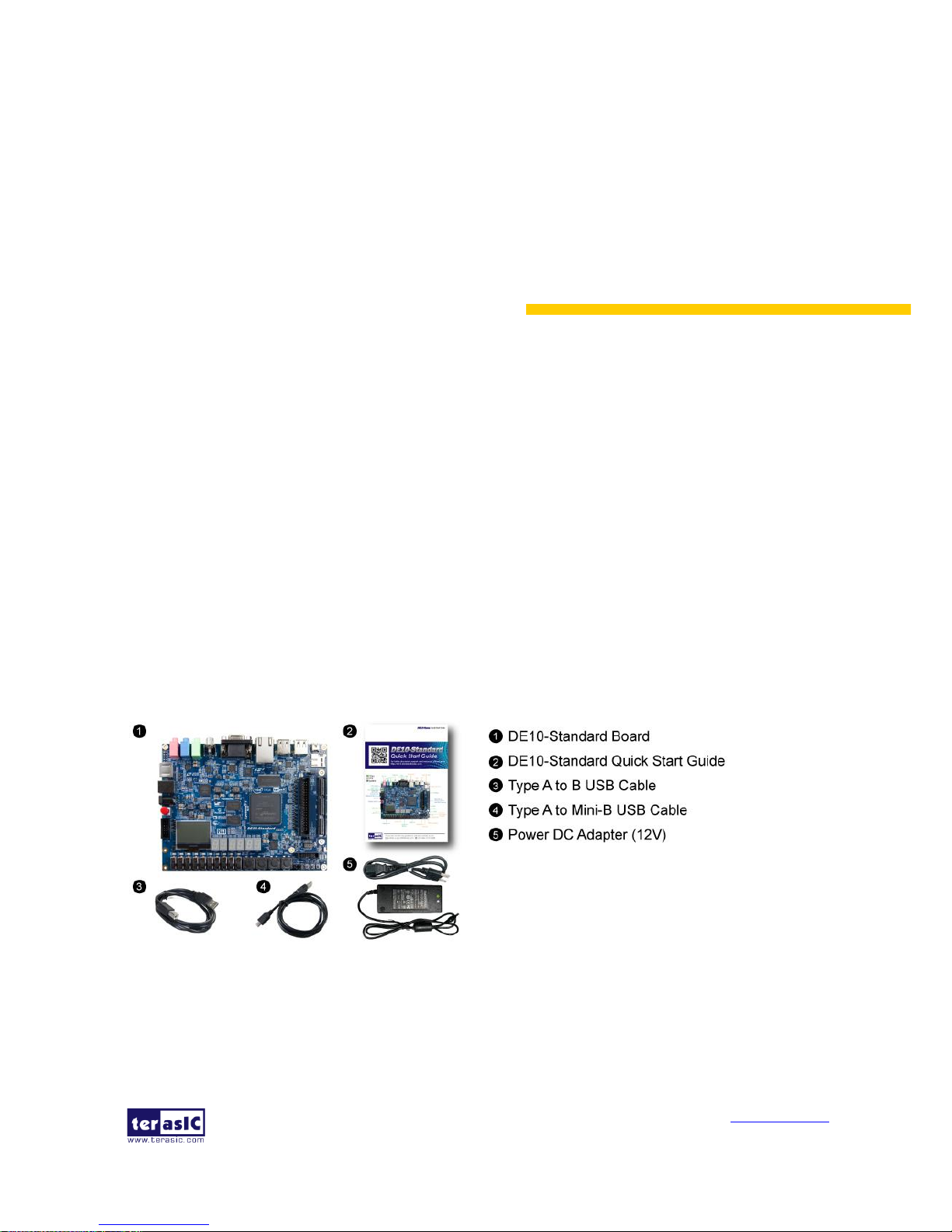
Figure 1-1 shows a photograph of the DE10-Standard package.
Page 6
DE10-Standard
User Manual
5
www.terasic.com
January 19, 2017
Figure 1-1 The DE10-Standard package contents
The DE10-Standard package includes:
The DE10-Standard development board
DE10-Standard Quick Start Guide
USB cable (Type A to B) for FPGA programming and control
USB cable (Type A to Mini-B) for UART control
12V DC power adapter
11..2
2
DDEE1100--SSttaannddaarrdd SSyysstteemm CCDD
The DE10-Standard System CD contains all the documents and supporting materials associated
with DE10-Standard, including the user manual, system builder, reference designs, and device
datasheets. Users can download this system CD from the link: http://de10-standard.terasic.com/cd/.
11..3
3
GGeettttiinngg HHeellpp
Here are the addresses where you can get help if you encounter any problems:
Terasic Technologies
9F., No.176, Sec.2, Gongdao 5th Rd, East Dist, Hsinchu City, 30070. Taiwan
Email: support@terasic.com
Tel.: +886-3-575-0880
Website: de10-standard.terasic.com
Page 7

DE10-Standard
User Manual
6
www.terasic.com
January 19, 2017
Page 8
DE10-Standard
User Manual
7
www.terasic.com
January 19, 2017
Chapter 2
Introduction of the
DE10-Standard Board
This chapter provides an introduction to the features and design characteristics of the board.
22..1
1
LLaayyoouutt aanndd CCoommppoonneennttss
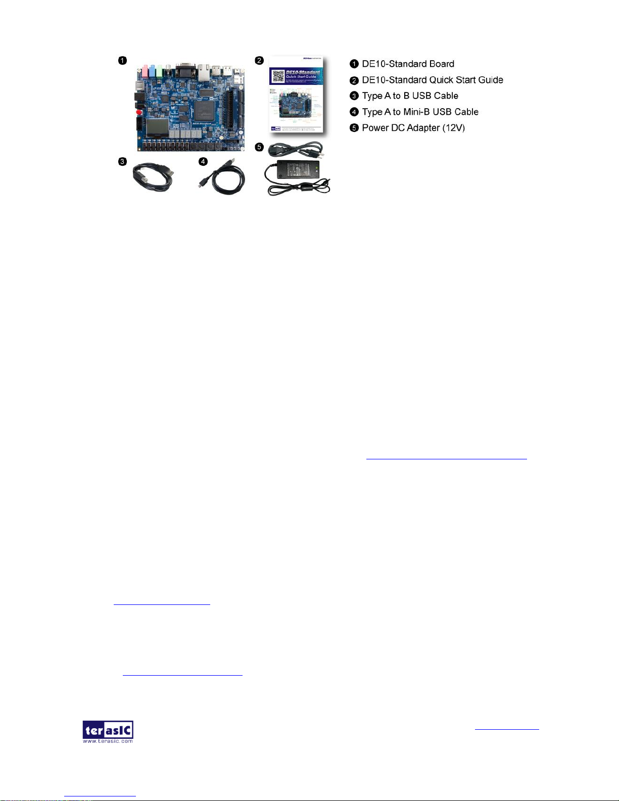
Figure 2-1 shows a photograph of the board. It depicts the layout of the board and indicates the
location of the connectors and key components.
Figure 2-1 DE10-Standard development board (top view)
Page 9
DE10-Standard
User Manual
8
www.terasic.com
January 19, 2017
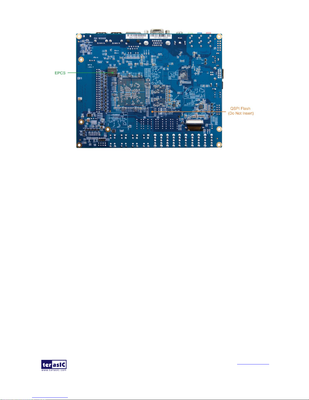
Figure 2-2 DE10-Standard development board (bottom view)
The DE10-Standard board has many features that allow users to implement a wide range of
designed circuits, from simple circuits to various multimedia projects.
The following hardware is provided on the board:
FPGA
Altera Cyclone® V SE 5CSXFC6D6F31C6N device
Altera serial configuration device – EPCS128
USB-Blaster II onboard for programming; JTAG Mode
64MB SDRAM (16-bit data bus)
4 push-buttons
10 slide switches
10 red user LEDs
Six 7-segment displays
Four 50MHz clock sources from the clock generator
24-bit CD-quality audio CODEC with line-in, line-out, and microphone-in jacks
VGA DAC (8-bit high-speed triple DACs) with VGA-out connector
TV decoder (NTSC/PAL/SECAM) and TV-in connector
PS/2 mouse/keyboard connector
IR receiver and IR emitter
One HSMC with Configurable I/O standard 1.5/1.8/2.5/3.3
One 40-pin expansion header with diode protection
Page 10

DE10-Standard
User Manual
9
www.terasic.com
January 19, 2017
A/D converter, 4-pin SPI interface with FPGA
HPS (Hard Processor System)
800MHz Dual-core ARM Cortex-A9 MPCore processor
1GB DDR3 SDRAM (32-bit data bus)
1 Gigabit Ethernet PHY with RJ45 connector
2-port USB Host, normal Type-A USB connector
Micro SD card socket
Accelerometer (I2C interface + interrupt)
UART to USB, USB Mini-B connector
Warm reset button and cold reset button
One user button and one user LED
LTC 2x7 expansion header
128x64 dots LCD Module with Backlight
22..2
2
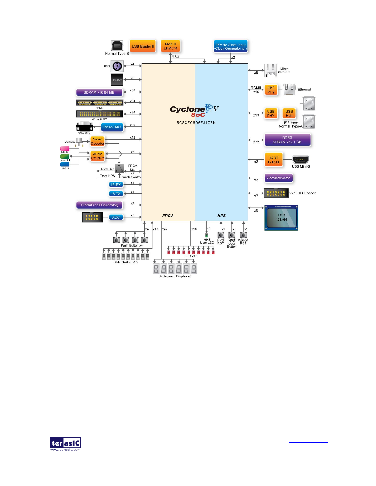
BBlloocckk DDiiaaggrraamm ooff tthhee DDEE1100--SSttaannddaarrdd BBooaarrdd
Figure 2-3 is the block diagram of the board. All the connections are established through the
Cyclone V SoC FPGA device to provide maximum flexibility for users. Users can configure the
FPGA to implement any system design.
Page 11
DE10-Standard
User Manual
10
www.terasic.com
January 19, 2017
Figure 2-3 Block diagram of DE10-Standard
Detailed information about Figure 2-3 are listed below.
FFPPGGAA DDeevviiccee
Cyclone V SoC 5CSXFC6D6F31C6N Device
Dual-core ARM Cortex-A9 (HPS)
110K programmable logic elements
5,140 Kbits embedded memory
6 fractional PLLs
2 hard memory controllers
3.125G transceivers
CCoonnffiigguurraattiioonn aanndd DDeebbuug
g
Page 12

DE10-Standard
User Manual
11
www.terasic.com
January 19, 2017
Quad serial configuration device – EPCS128 on FPGA
Onboard USB-Blaster II (normal type B USB connector)
MMeemmoorryy DDeevviiccee
64MB (32Mx16) SDRAM on FPGA
1GB (2x256Mx16) DDR3 SDRAM on HPS
Micro SD card socket on HPS
CCoommmmuunniiccaattiioonn
Two port USB 2.0 Host (ULPI interface with USB type A connector)
UART to USB (USB Mini-B connector)
10/100/1000 Ethernet
PS/2 mouse/keyboard
IR emitter/receiver
I2C multiplexer
CCoonnnneeccttoorrss
One HSMC (8-channel Transceivers, Configurable I/O standards 1.5/1.8/2.5/3.3V)
One 40-pin expansion headers
One 10-pin ADC input header
One LTC connector (one Serial Peripheral Interface (SPI) Master ,one I2C and one GPIO
interface )
DDiissppllaayy
24-bit VGA DAC
128x64 dots LCD Module with Backlight
AAuuddiioo
24-bit CODEC, Line-in, Line-out, and microphone-in jacks
VViiddeeoo IInnppuutt
TV decoder (NTSC/PAL/SECAM) and TV-in connector
AADDCC
Interface: SPI
Fast throughput rate: 500 KSPS
Channel number: 8
Resolution: 12-bit
Page 13

DE10-Standard
User Manual
12
www.terasic.com
January 19, 2017
Analog input range : 0 ~ 4.096
SSwwiittcchheess,, BBuuttttoonnss,, aanndd IInnddiiccaattoorrss
5 user Keys (FPGA x4, HPS x1)
10 user switches (FPGA x10)
11 user LEDs (FPGA x10, HPS x 1)
2 HPS reset buttons (HPS_RESET_n and HPS_WARM_RST_n)
Six 7-segment displays
SSeennssoorrss
G-Sensor on HPS
PPoowweerr
12V DC input
Page 14
DE10-Standard
User Manual
13
www.terasic.com
January 19, 2017
Chapter 3
Using the
DE10-Standard Board
This chapter provides an instruction to use the board and describes the peripherals.
33..1
1
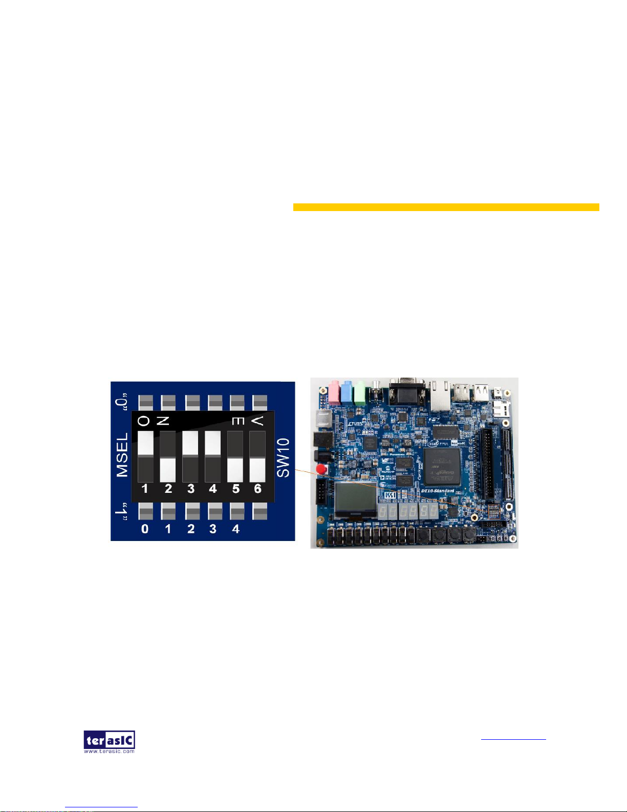
SSeettttiinnggss ooff FFPPGGAA CCoonnffiigguurraattiioonn MMooddee
When the DE10-Standard board is powered on, the FPGA can be configured from EPCS or HPS.
The MSEL[4:0] pins are used to select the configuration scheme. It is implemented as a 6-pin DIP
switch SW10 on the DE10-Standard board, as shown in Figure 3-1.
Figure 3-1 DIP switch (SW10) setting of Active Serial (AS) mode on DE10-Standard board
Table 3-1 shows the relation between MSEL[4:0] and DIP switch (SW10).
Page 15

DE10-Standard
User Manual
14
www.terasic.com
January 19, 2017
Table 3-1 FPGA Configuration Mode Switch (SW10)
Board Reference
Signal Name
Description
Default
AS Mode
SW10.1
MSEL0
Use these pins to set the FPGA
Configuration scheme
OFF (“1”)
SW10.2
MSEL1
ON (“0”)
SW10.3
MSEL2
ON (“0”)
SW10.4
MSEL3
OFF (“1”)
SW10.5
MSEL4
ON (“0”)
SW10.6
N/A
N/A
N/A
Figure 3-1 shows MSEL[4:0] setting of AS mode, which is also the default setting on
DE10-Standard. When the board is powered on, the FPGA is configured from EPCS, which is
pre-programmed with the default code. If developers wish to reconfigure FPGA from an application
software running on Linux, the MSEL[4:0] needs to be set to “01010” before the programming
process begins.
Table 3-2 MSEL Pin Settings for FPGA Configure of DE10-Standard
MSEL[4:0]
Configure Scheme
Description
10010
AS
FPGA configured from EPCS (default)
01010
FPPx32
FPGA configured from HPS software: Linux
33..2
2
CCoonnffiigguurraattiioonn ooff CCyycclloonnee VV SSooCC FFPPGGAA oonn DDEE1100--SSttaannddaarrdd
There are two types of programming method supported by DE10-Standard:
1. JTAG programming: It is named after the IEEE standards Joint Test Action Group.
The configuration bit stream is downloaded directly into the Cyclone V SoC FPGA. The FPGA will
retain its current status as long as the power keeps applying to the board; the configuration
information will be lost when the power is off.
2. AS programming: The other programming method is Active Serial configuration.
The configuration bit stream is downloaded into the quad serial configuration device (EPCS128),
which provides non-volatile storage for the bit stream. The information is retained within EPCS128
even if the DE10-Standard board is turned off. When the board is powered on, the configuration
data in the EPCS128 device is automatically loaded into the Cyclone V SoC FPGA.
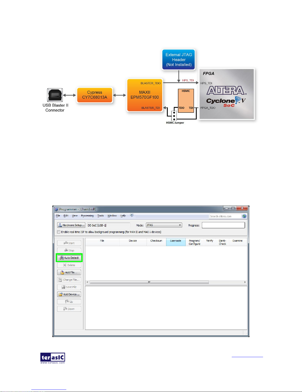
JTAG Chain on DE10-Standard Board
The FPGA device can be configured through JTAG interface on DE10-Standard board, but the
Page 16
DE10-Standard
User Manual
15
www.terasic.com
January 19, 2017
JTAG chain must form a closed loop, which allows Quartus II programmer to the detect FPGA
device. Figure 3-2 illustrates the JTAG chain on DE10-Standard board.
Figure 3-2 Path of the JTAG chain
Configure the FPGA in JTAG Mode
There are two devices (FPGA and HPS) on the JTAG chain. The following shows how the FPGA is
programmed in JTAG mode step by step.
1. Open the Quartus II programmer and click “Auto Detect”, as circled in Figure 3-3
Page 17
DE10-Standard
User Manual
16
www.terasic.com
January 19, 2017
Figure 3-3 Detect FPGA device in JTAG mode
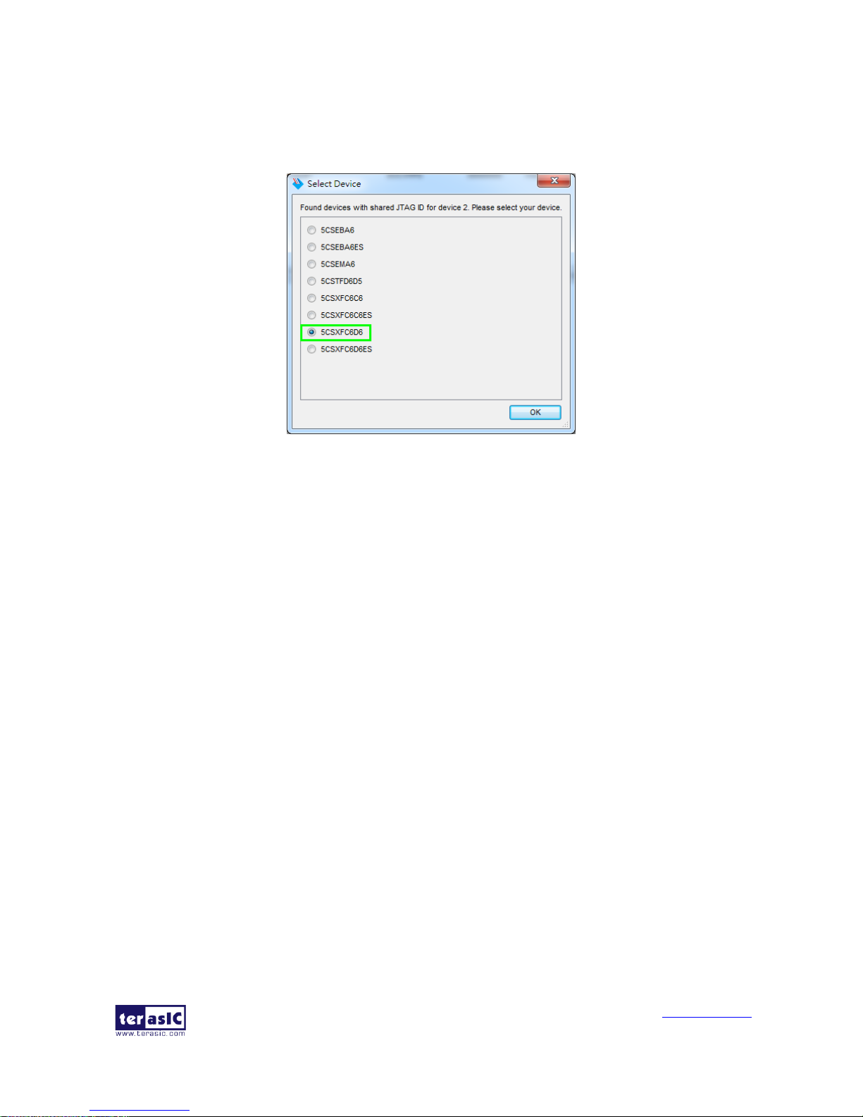
2. Select detected device associated with the board, as circled in Figure 3-4.
Figure 3-4 Select 5CSXFC6D6 device
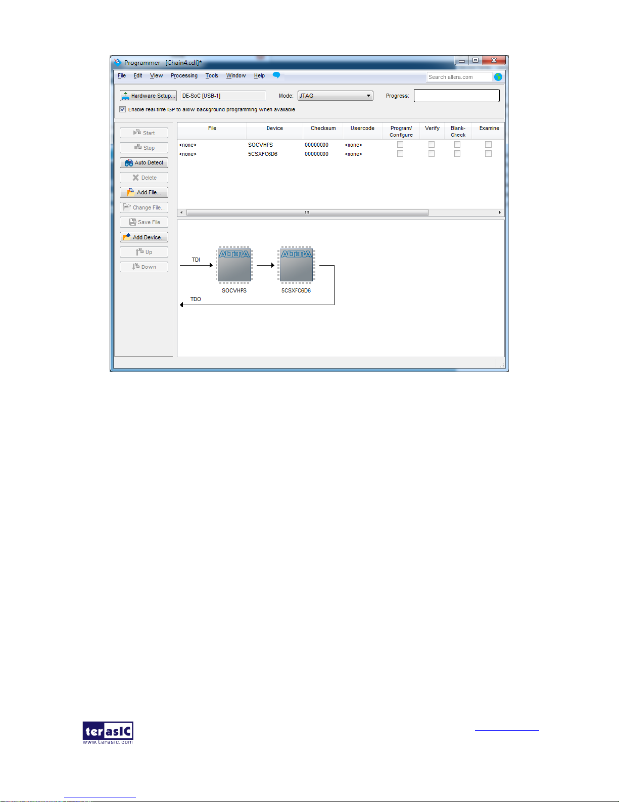
3. Both FPGA and HPS are detected, as shown in Figure 3-5.
Page 18
DE10-Standard
User Manual
17
www.terasic.com
January 19, 2017
Figure 3-5 FPGA and HPS detected in Quartus programmer
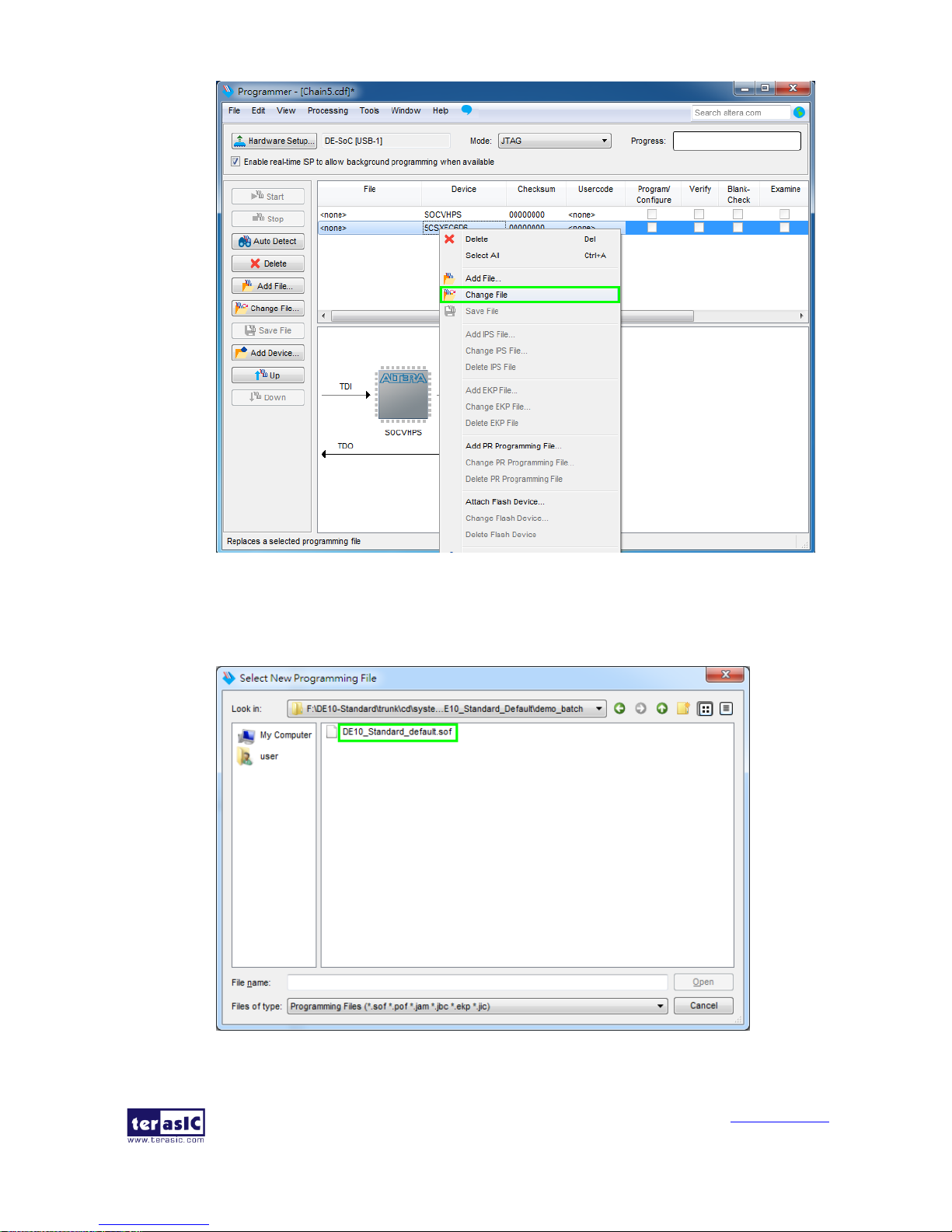
4. Right click on the FPGA device and open the .sof file to be programmed, as highlighted in
Figure 3-6.
Page 19
DE10-Standard
User Manual
18
www.terasic.com
January 19, 2017
Figure 3-6 Open the .sof file to be programmed into the FPGA device
5. Select the .sof file to be programmed, as shown in Figure 3-7.
Figure 3-7 Select the .sof file to be programmed into the FPGA device
Page 20
DE10-Standard
User Manual
19
www.terasic.com
January 19, 2017
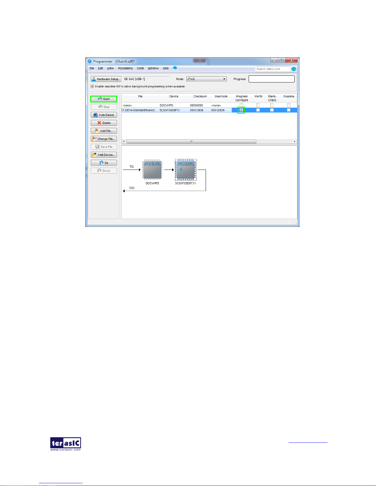
6. Click “Program/Configure” check box and then click “Start” button to download the .sof file
into the FPGA device, as shown in Figure 3-8.
Figure 3-8 Program .sof file into the FPGA device
Configure the FPGA in AS Mode
The DE10-Standard board uses a quad serial configuration device (EPCS128) to store
configuration data for the Cyclone V SoC FPGA. This configuration data is automatically
loaded from the quad serial configuration device chip into the FPGA when the board is
powered up.
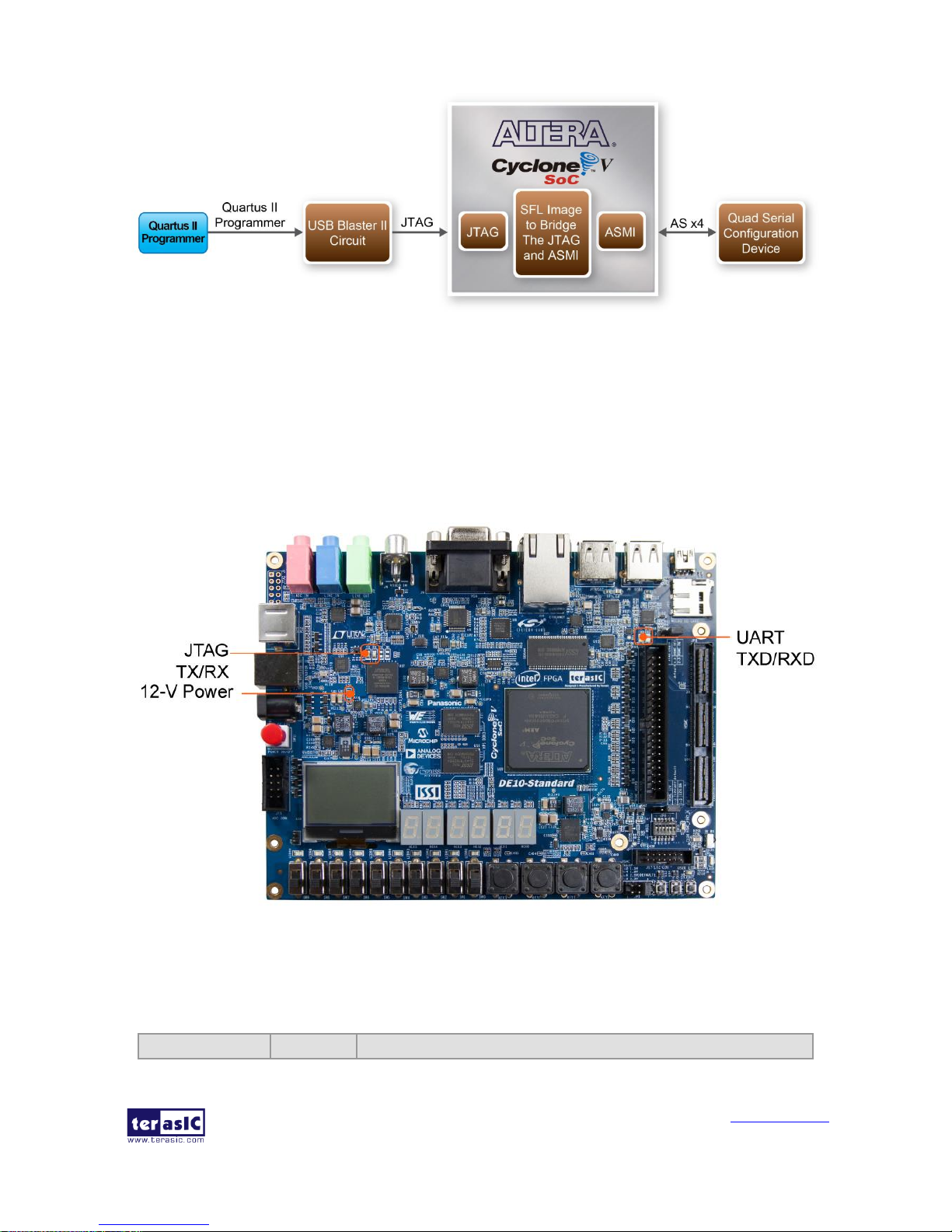
Users need to use Serial Flash Loader (SFL) to program the quad serial configuration device
via JTAG interface. The FPGA-based SFL is a soft intellectual property (IP) core within the
FPGA that bridge the JTAG and Flash interfaces. The SFL Megafunction is available in
Quartus II. Figure 3-9 shows the programming method when adopting SFL solution.
Please refer to Chapter 9: Steps of Programming the Quad Serial Configuration Device for the
basic programming instruction on the serial configuration device.
Page 21
DE10-Standard
User Manual
20
www.terasic.com
January 19, 2017
Figure 3-9 Programming a quad serial configuration device with SFL solution
33..3
3
BBooaarrdd SSttaattuuss EElleemmeennttss
In addition to the 10 LEDs that FPGA device can control, there are 5 indicators which can indicate
the board status (See Figure 3-10), please refer the details in Table 3-3
Figure 3-10 LED Indicators on DE10-Standard
Table 3-3 LED Indicators
Board Reference
LED Name
Description
Page 22
DE10-Standard
User Manual
21
www.terasic.com
January 19, 2017
D14
12-V Power
Illuminate when 12V power is active.
TXD
UART TXD
Illuminate when data is transferred from FT232R to USB Host.
RXD
UART RXD
Illuminate when data is transferred from USB Host to FT232R.
D5
JTAG_RX
Reserved
D4
JTAG_TX
33..4
4
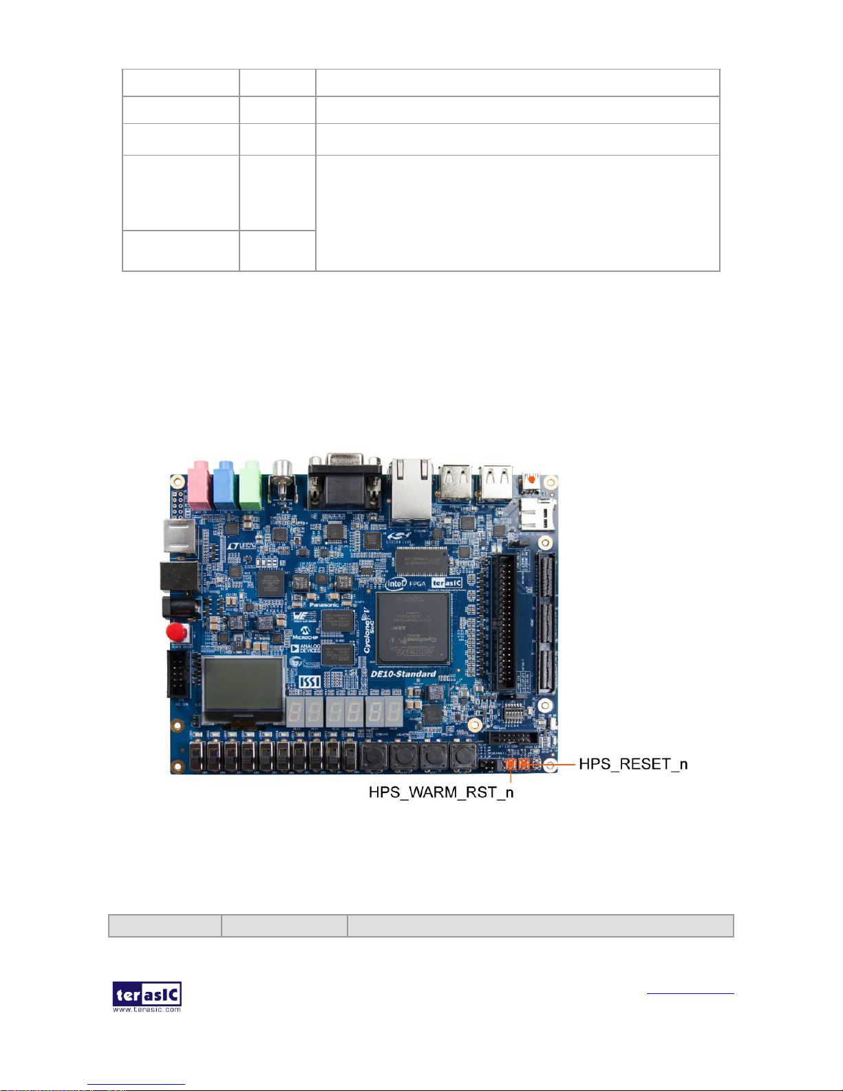
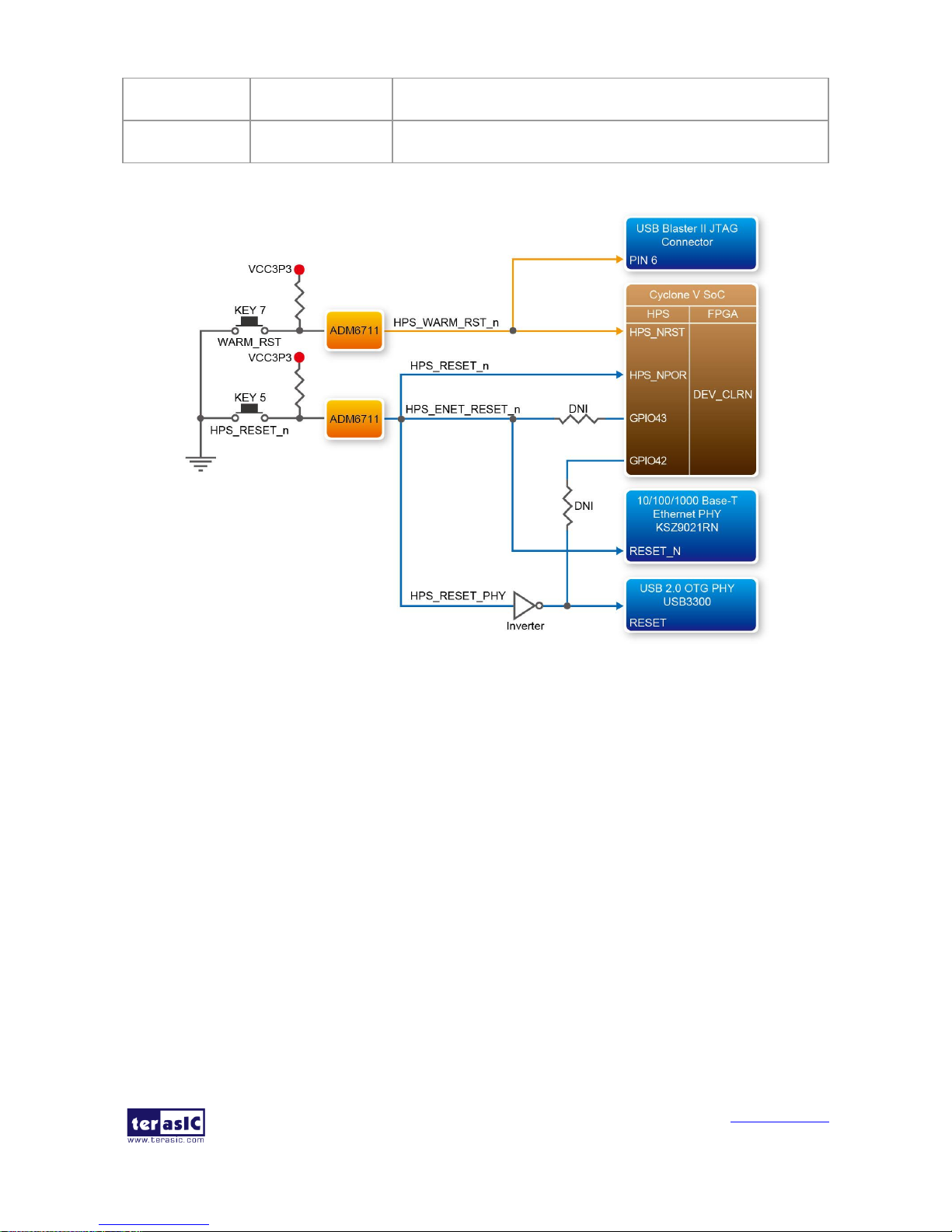
BBooaarrdd RReesseett EElleemmeennttss
There are two HPS reset buttons on DE10-Standard, HPS (cold) reset and HPS warm reset, as
shown in Figure 3-11. Table 3-4 describes the purpose of these two HPS reset buttons. Figure 3-12
is the reset tree for DE10-Standard.
Figure 3-11 HPS cold reset and warm reset buttons on DE10-Standard
Table 3-4 Description of Two HPS Reset Buttons on DE10-Standard
Board Reference
Signal Name
Description
Page 23
DE10-Standard
User Manual
22
www.terasic.com
January 19, 2017
KEY5
HPS_RESET_N
Cold reset to the HPS, Ethernet PHY and USB host device.
Active low input which resets all HPS logics that can be reset.
KEY7
HPS_WARM_RST_N
Warm reset to the HPS block. Active low input affects the
system reset domain for debug purpose.
Figure 3-12 HPS reset tree on DE10-Standard board
33..5
5
CClloocckk CCiirrccuuiittrryy
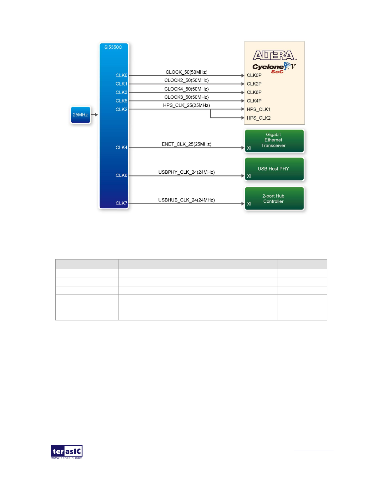
Figure 3-13 shows the default frequency of all external clocks to the Cyclone V SoC FPGA. A
clock generator is used to distribute clock signals with low jitter. The four 50MHz clock signals
connected to the FPGA are used as clock sources for user logic. One 25MHz clock signal is
connected to two HPS clock inputs, and the other one is connected to the clock input of Gigabit
Ethernet Transceiver. Two 24MHz clock signals are connected to the clock inputs of USB
Host/OTG PHY and USB hub controller. The associated pin assignment for clock inputs to FPGA
I/O pins is listed in Table 3-5.
Page 24
DE10-Standard
User Manual
23
www.terasic.com
January 19, 2017
Figure 3-13 Block diagram of the clock distribution on DE10-Standard
Table 3-5 Pin Assignment of Clock Inputs
Signal Name
FPGA Pin No.
Description
I/O Standard
CLOCK_50
PIN_AF14
50 MHz clock input
3.3V
CLOCK2_50
PIN_AA16
50 MHz clock input
3.3V
CLOCK3_50
PIN_Y26
50 MHz clock input
3.3V
CLOCK4_50
PIN_K14
50 MHz clock input
3.3V
HPS_CLOCK1_25
PIN_D25
25 MHz clock input
3.3V
HPS_CLOCK2_25
PIN_F25
25 MHz clock input
3.3V
33..6
6
PPeerriipphheerraallss CCoonnnneecctteedd ttoo tthhee FFPPGGAA
This section describes the interfaces connected to the FPGA. Users can control or monitor different
interfaces with user logic from the FPGA.
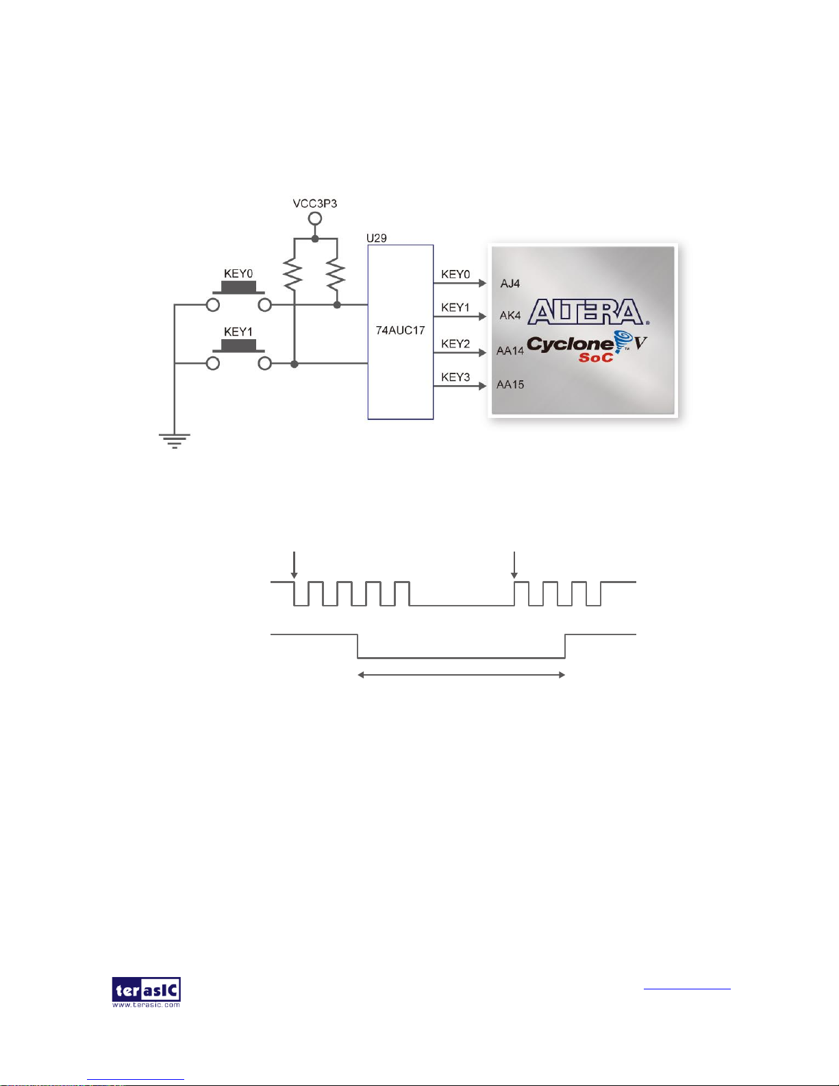
3.6.1 User Push-buttons, Switches and LEDs
The board has four push-buttons connected to the FPGA, as shown in Figure 3-14 Connections
between the push-buttons and the Cyclone V SoC FPGA. Schmitt trigger circuit is implemented and act
Page 25
DE10-Standard
User Manual
24
www.terasic.com
January 19, 2017
as switch debounce in Figure 3-15 for the push-buttons connected. The four push-buttons named
KEY0, KEY1, KEY2, and KEY3 coming out of the Schmitt trigger device are connected directly to
the Cyclone V SoC FPGA. The push-button generates a low logic level or high logic level when it
is pressed or not, respectively. Since the push-buttons are debounced, they can be used as clock or
reset inputs in a circuit.
Figure 3-14 Connections between the push-buttons and the Cyclone V SoC FPGA
Pushbutton releasedPushbutton depressed
Before
Debouncing
Schmitt Trigger
Debounced
Figure 3-15 Switch debouncing
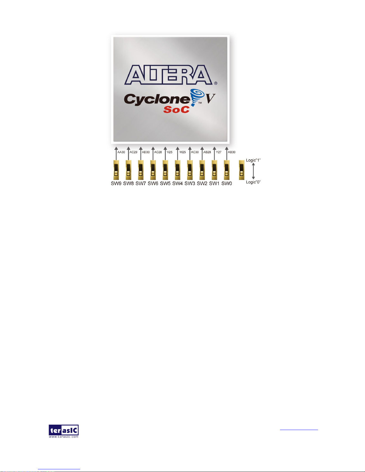
There are ten slide switches connected to the FPGA, as shown in Figure 3-16. These switches are
not debounced and to be used as level-sensitive data inputs to a circuit. Each switch is connected
directly and individually to the FPGA. When the switch is set to the DOWN position (towards the
edge of the board), it generates a low logic level to the FPGA. When the switch is set to the UP
position, a high logic level is generated to the FPGA
Page 26
DE10-Standard
User Manual
25
www.terasic.com
January 19, 2017
.
Figure 3-16 Connections between the slide switches and the Cyclone V SoC FPGA
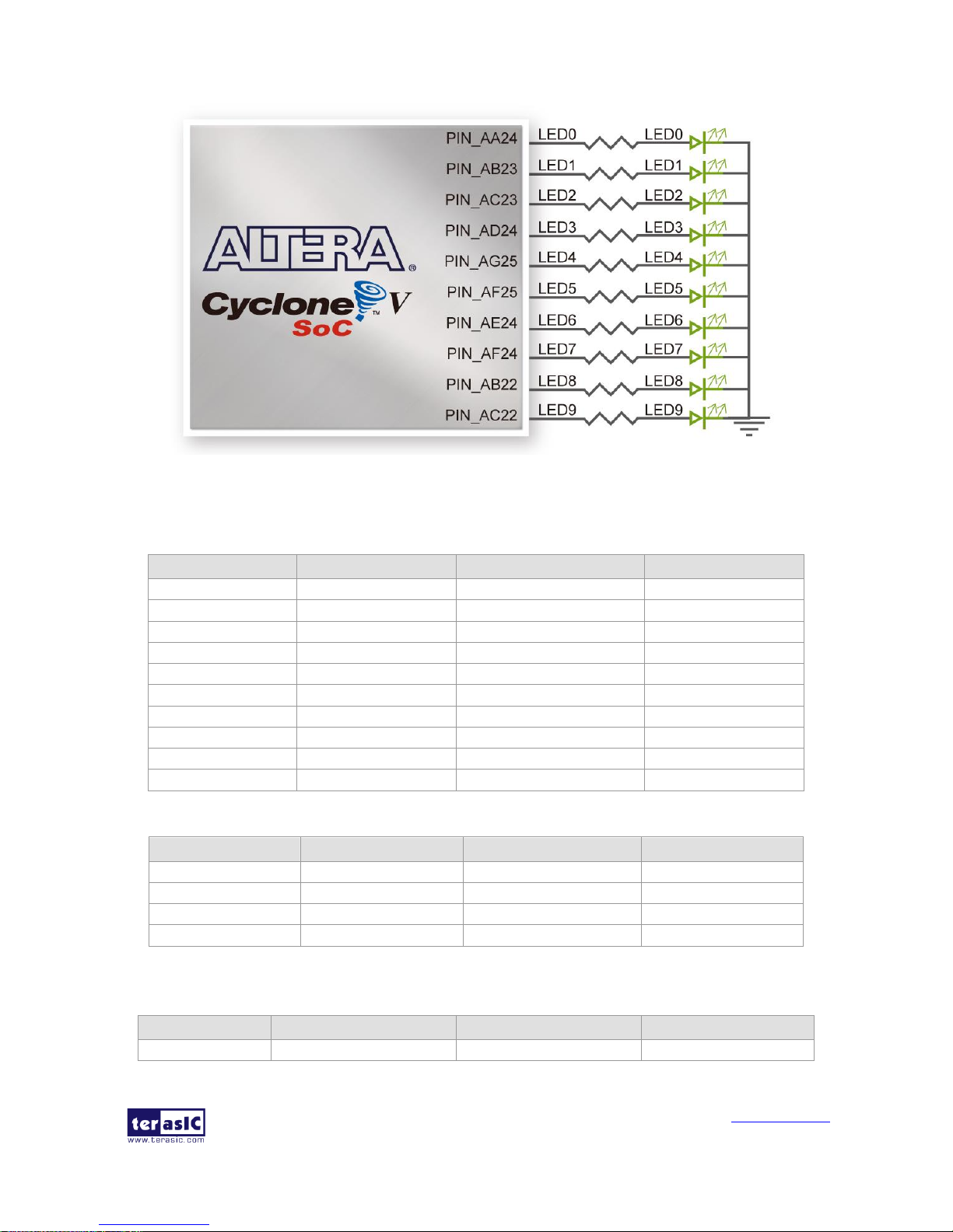
There are also ten user-controllable LEDs connected to the FPGA. Each LED is driven directly and
individually by the Cyclone V SoC FPGA; driving its associated pin to a high logic level or low
level to turn the LED on or off, respectively. Figure 3-17 shows the connections between LEDs and
Cyclone V SoC FPGA. Table 3-6, Table 3-7 and Table 3-8 list the pin assignment of user
push-buttons, switches, and LEDs.
Page 27
DE10-Standard
User Manual
26
www.terasic.com
January 19, 2017
Figure 3-17 Connections between the LEDs and the Cyclone V SoC FPGA
Table 3-6 Pin Assignment of Slide Switches
Signal Name
FPGA Pin No.
Description
I/O Standard
SW[0]
PIN_AB30
Slide Switch[0]
Depend on JP3
SW[1]
PIN_Y27
Slide Switch[1]
Depend on JP3
SW[2]
PIN_AB28
Slide Switch[2]
Depend on JP3
SW[3]
PIN_AC30
Slide Switch[3]
Depend on JP3
SW[4]
PIN_W25
Slide Switch[4]
Depend on JP3
SW[5]
PIN_V25
Slide Switch[5]
Depend on JP3
SW[6]
PIN_AC28
Slide Switch[6]
Depend on JP3
SW[7]
PIN_AD30
Slide Switch[7]
Depend on JP3
SW[8]
PIN_AC29
Slide Switch[8]
Depend on JP3
SW[9]
PIN_AA30
Slide Switch[9]
Depend on JP3
Table 3-7 Pin Assignment of Push-buttons
Signal Name
FPGA Pin No.
Description
I/O Standard
KEY[0]
PIN_AJ4
Push-button[0]
3.3V
KEY[1]
PIN_AK4
Push-button[1]
3.3V
KEY[2]
PIN_AA14
Push-button[2]
3.3V
KEY[3]
PIN_AA15
Push-button[3]
3.3V
Table 3-8 Pin Assignment of LEDs
Signal Name
FPGA Pin No.
Description
I/O Standard
LEDR[0]
PIN_AA24
LED [0]
3.3V
Page 28
DE10-Standard
User Manual
27
www.terasic.com
January 19, 2017
LEDR[1]
PIN_AB23
LED [1]
3.3V
LEDR[2]
PIN_AC23
LED [2]
3.3V
LEDR[3]
PIN_AD24
LED [3]
3.3V
LEDR[4]
PIN_AG25
LED [4]
3.3V
LEDR[5]
PIN_AF25
LED [5]
3.3V
LEDR[6]
PIN_AE24
LED [6]
3.3V
LEDR[7]
PIN_AF24
LED [7]
3.3V
LEDR[8]
PIN_AB22
LED [8]
3.3V
LEDR[9]
PIN_AC22
LED [9]
3.3V
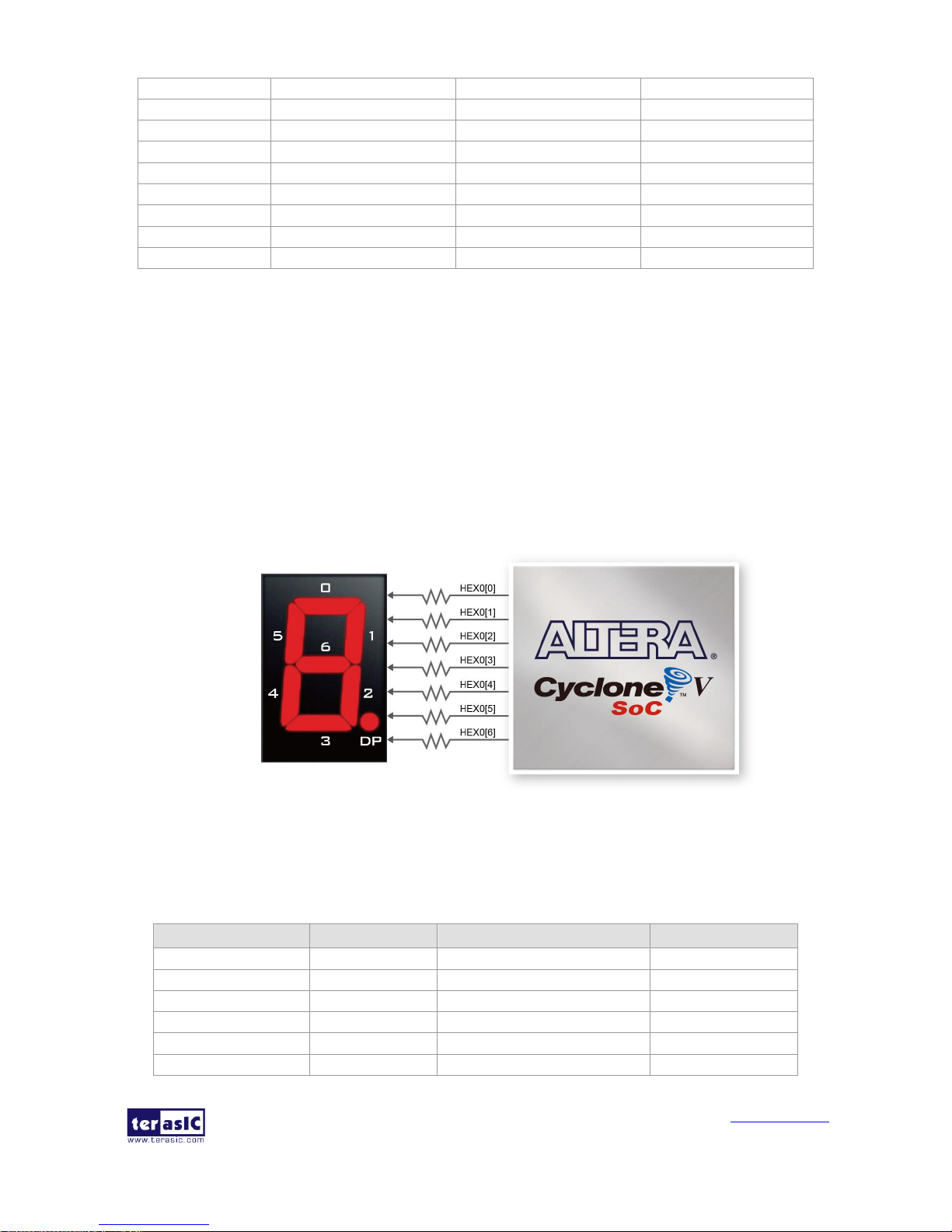
3.6.2 7-segment Displays
The DE10-Standard board has six 7-segment displays. These displays are paired to display numbers
in various sizes. Figure 3-18 shows the connection of seven segments (common anode) to pins on
Cyclone V SoC FPGA. The segment can be turned on or off by applying a low logic level or high
logic level from the FPGA, respectively.
Each segment in a display is indexed from 0 to 6, with corresponding positions given in Figure
3-18. Table 3-9 shows the pin assignment of FPGA to the 7-segment displays.
Figure 3-18 Connections between the 7-segment display HEX0 and the Cyclone V SoC FPGA
Table 3-9 Pin Assignment of 7-segment Displays
Signal Name
FPGA Pin No.
Description
I/O Standard
HEX0[0]
PIN_W17
Seven Segment Digit 0[0]
3.3V
HEX0[1]
PIN_V18
Seven Segment Digit 0[1]
3.3V
HEX0[2]
PIN_AG17
Seven Segment Digit 0[2]
3.3V
HEX0[3]
PIN_AG16
Seven Segment Digit 0[3]
3.3V
HEX0[4]
PIN_AH17
Seven Segment Digit 0[4]
3.3V
HEX0[5]
PIN_AG18
Seven Segment Digit 0[5]
3.3V
Page 29
DE10-Standard
User Manual
28
www.terasic.com
January 19, 2017
HEX0[6]
PIN_AH18
Seven Segment Digit 0[6]
3.3V
HEX1[0]
PIN_AF16
Seven Segment Digit 1[0]
3.3V
HEX1[1]
PIN_V16
Seven Segment Digit 1[1]
3.3V
HEX1[2]
PIN_AE16
Seven Segment Digit 1[2]
3.3V
HEX1[3]
PIN_AD17
Seven Segment Digit 1[3]
3.3V
HEX1[4]
PIN_AE18
Seven Segment Digit 1[4]
3.3V
HEX1[5]
PIN_AE17
Seven Segment Digit 1[5]
3.3V
HEX1[6]
PIN_V17
Seven Segment Digit 1[6]
3.3V
HEX2[0]
PIN_AA21
Seven Segment Digit 2[0]
3.3V
HEX2[1]
PIN_AB17
Seven Segment Digit 2[1]
3.3V
HEX2[2]
PIN_AA18
Seven Segment Digit 2[2]
3.3V
HEX2[3]
PIN_Y17
Seven Segment Digit 2[3]
3.3V
HEX2[4]
PIN_Y18
Seven Segment Digit 2[4]
3.3V
HEX2[5]
PIN_AF18
Seven Segment Digit 2[5]
3.3V
HEX2[6]
PIN_W16
Seven Segment Digit 2[6]
3.3V
HEX3[0]
PIN_Y19
Seven Segment Digit 3[0]
3.3V
HEX3[1]
PIN_W19
Seven Segment Digit 3[1]
3.3V
HEX3[2]
PIN_AD19
Seven Segment Digit 3[2]
3.3V
HEX3[3]
PIN_AA20
Seven Segment Digit 3[3]
3.3V
HEX3[4]
PIN_AC20
Seven Segment Digit 3[4]
3.3V
HEX3[5]
PIN_AA19
Seven Segment Digit 3[5]
3.3V
HEX3[6]
PIN_AD20
Seven Segment Digit 3[6]
3.3V
HEX4[0]
PIN_AD21
Seven Segment Digit 4[0]
3.3V
HEX4[1]
PIN_AG22
Seven Segment Digit 4[1]
3.3V
HEX4[2]
PIN_AE22
Seven Segment Digit 4[2]
3.3V
HEX4[3]
PIN_AE23
Seven Segment Digit 4[3]
3.3V
HEX4[4]
PIN_AG23
Seven Segment Digit 4[4]
3.3V
HEX4[5]
PIN_AF23
Seven Segment Digit 4[5]
3.3V
HEX4[6]
PIN_AH22
Seven Segment Digit 4[6]
3.3V
HEX5[0]
PIN_AF21
Seven Segment Digit 5[0]
3.3V
HEX5[1]
PIN_AG21
Seven Segment Digit 5[1]
3.3V
HEX5[2]
PIN_AF20
Seven Segment Digit 5[2]
3.3V
HEX5[3]
PIN_AG20
Seven Segment Digit 5[3]
3.3V
HEX5[4]
PIN_AE19
Seven Segment Digit 5[4]
3.3V
HEX5[5]
PIN_AF19
Seven Segment Digit 5[5]
3.3V
HEX5[6]
PIN_AB21
Seven Segment Digit 5[6]
3.3V
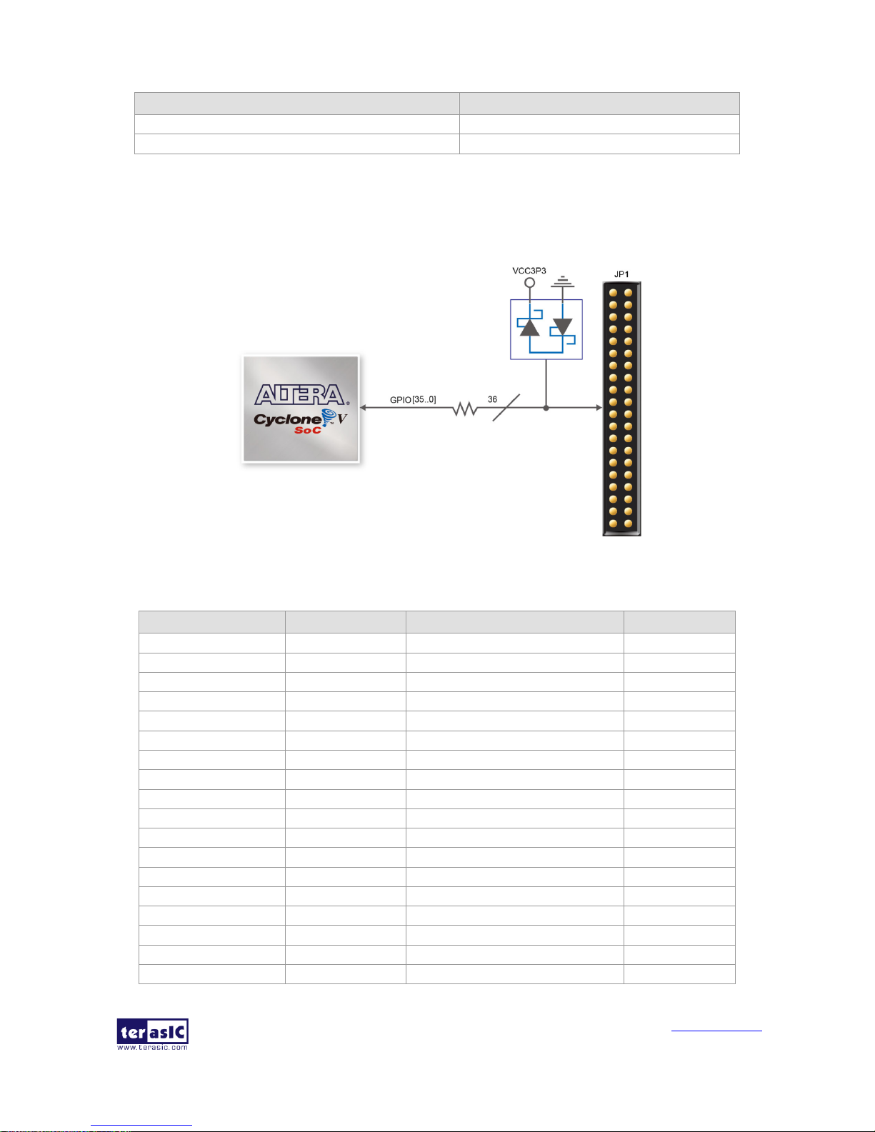
3.6.3 2x20 GPIO Expansion Header
The board has one 40-pin expansion headers. Thw header has 36 user pins connected directly to the
Cyclone V SoC FPGA. It also comes with DC +5V (VCC5), DC +3.3V (VCC3P3), and two GND
pins. The maximum power consumption allowed for a daughter card connected to one GPIO ports
is shown in Table 3-10.
Page 30
DE10-Standard
User Manual
29
www.terasic.com
January 19, 2017
Table 3-10 Voltage and Max. Current Limit of Expansion Header(s)
Supplied Voltage
Max. Current Limit
5V
1A
3.3V
1.5A
Each pin on the expansion headers is connected to two diodes and a resistor for protection against
high or low voltage level. Figure 3-19 shows the protection circuitry applied to all 36 data pins.
Table 3-11 shows the pin assignment of the GPIO header.
Figure 3-19 Connections between the GPIO header and Cyclone V SoC FPGA
Table 3-11 Pin Assignment of Expansion Headers
Signal Name
FPGA Pin No.
Description
I/O Standard
GPIO[0]
PIN_W15
GPIO Connection 0[0]
3.3V
GPIO[1]
PIN_AK2
GPIO Connection 0[1]
3.3V
GPIO[2]
PIN_Y16
GPIO Connection 0[2]
3.3V
GPIO[3]
PIN_AK3
GPIO Connection 0[3]
3.3V
GPIO[4]
PIN_AJ1
GPIO Connection 0[4]
3.3V
GPIO[5]
PIN_AJ2
GPIO Connection 0[5]
3.3V
GPIO[6]
PIN_AH2
GPIO Connection 0[6]
3.3V
GPIO[7]
PIN_AH3
GPIO Connection 0[7]
3.3V
GPIO[8]
PIN_AH4
GPIO Connection 0[8]
3.3V
GPIO[9]
PIN_AH5
GPIO Connection 0[9]
3.3V
GPIO[10]
PIN_AG1
GPIO Connection 0[10]
3.3V
GPIO[11]
PIN_AG2
GPIO Connection 0[11]
3.3V
GPIO[12]
PIN_AG3
GPIO Connection 0[12]
3.3V
GPIO[13]
PIN_AG5
GPIO Connection 0[13]
3.3V
GPIO[14]
PIN_AG6
GPIO Connection 0[14]
3.3V
GPIO[15]
PIN_AG7
GPIO Connection 0[15]
3.3V
GPIO[16]
PIN_AG8
GPIO Connection 0[16]
3.3V
GPIO[17]
PIN_AF4
GPIO Connection 0[17]
3.3V
Page 31

DE10-Standard
User Manual
30
www.terasic.com
January 19, 2017
GPIO[18]
PIN_AF5
GPIO Connection 0[18]
3.3V
GPIO[19]
PIN_AF6
GPIO Connection 0[19]
3.3V
GPIO[20]
PIN_AF8
GPIO Connection 0[20]
3.3V
GPIO[21]
PIN_AF9
GPIO Connection 0[21]
3.3V
GPIO[22]
PIN_AF10
GPIO Connection 0[22]
3.3V
GPIO[23]
PIN_AE7
GPIO Connection 0[23]
3.3V
GPIO[24]
PIN_AE9
GPIO Connection 0[24]
3.3V
GPIO[25]
PIN_AE11
GPIO Connection 0[25]
3.3V
GPIO[26]
PIN_AE12
GPIO Connection 0[26]
3.3V
GPIO[27]
PIN_AD7
GPIO Connection 0[27]
3.3V
GPIO[28]
PIN_AD9
GPIO Connection 0[28]
3.3V
GPIO[29]
PIN_AD10
GPIO Connection 0[29]
3.3V
GPIO[30]
PIN_AD11
GPIO Connection 0[30]
3.3V
GPIO[31]
PIN_AD12
GPIO Connection 0[31]
3.3V
GPIO[32]
PIN_AC9
GPIO Connection 0[32]
3.3V
GPIO[33]
PIN_AC12
GPIO Connection 0[33]
3.3V
GPIO[34]
PIN_AB12
GPIO Connection 0[34]
3.3V
GPIO[35]
PIN_AA12
GPIO Connection 0[35]
3.3V
3.6.4 HSMC connector
The board contains a High Speed Mezzanine Card (HSMC) interface to provide a mechanism for
extending the peripheral-set of an FPGA host board by means of add-on daughter cards, which can
address today’s high speed signaling requirements as well as low-speed device interface support.
The HSMC interface support JTAG, clock outputs and inputs, high-speed serial I/O (transceivers),
and single-ended or differential signaling. Signals on the HSMC port are shown in Figure 3-. Table
3-12 shows the maximum power consumption of the daughter card that connects to HSMC port.
Page 32

DE10-Standard
User Manual
31
www.terasic.com
January 19, 2017
Figure 3-20 HSMC Signal Bank Diagram
Table 3-12 Power Supply of the HSMC
Supplied Voltage
Max. Current Limit
12V
1A
3.3V
1.5A
The voltage level of the I/O pins on the HSMC connector can be adjusted to 3.3V, 2.5V, 1.8V, or
1.5V using JP3 (The default setting is 2.5V). Because the HSMC I/Os are connected to Bank 5B &
8A of the FPGA and the VCCIO voltage of these two banks are controlled by the header JP3, users
can use a jumper to select the input voltage of VCCIO5B & VCCIO8A to 3.3V, 2.5V, 1.8V, and
1.5V to control the voltage level of the I/O pins. Table 3- lists the jumper settings of the JP3. Table
3- shows all the pin assignments of the HSMC connector.
Table 3-13 Jumper Settings for different I/O Standards
JP3 Jumper Settings
Supplied Voltage to VCCIO5B &
VCCIO8A
IO Voltage of HSMC
Connector (JP2)
Short Pins 1 and 2
1.5V
1.5V
Short Pins 3 and 4
1.8V
1.8V
Short Pins 5 and 6
2.5V
2.5V (Default)
Short Pins 7 and 8
3.3V
3.3V
Table 3-13 Pin Assignments for HSMC connector
Signal Name
FPGA Pin No.
Description
I/O Standard
Page 33

DE10-Standard
User Manual
32
www.terasic.com
January 19, 2017
HSMC_CLKIN0
PIN_J14
Dedicated clock input
Depend on JP3
HSMC_CLKIN_N1
PIN_AB27
LVDS RX or CMOS I/O or
differential clock input
Depend on JP3
HSMC_CLKIN_N2
PIN_G15
LVDS RX or CMOS I/O or
differential clock input
Depend on JP3
HSMC_CLKIN_P1
PIN_AA26
LVDS RX or CMOS I/O or
differential clock input
Depend on JP3
HSMC_CLKIN_P2
PIN_H15
LVDS RX or CMOS I/O or
differential clock input
Depend on JP3
HSMC_CLKOUT0
PIN_AD29
Dedicated clock output
Depend on JP3
HSMC_CLKOUT_N1
PIN_E6
LVDS TX or CMOS I/O or
differential clock input/output
Depend on JP3
HSMC_CLKOUT_N2
PIN_A10
LVDS TX or CMOS I/O or
differential clock input/output
Depend on JP3
HSMC_CLKOUT_P1
PIN_E7
LVDS TX or CMOS I/O or
differential clock input/output
Depend on JP3
HSMC_CLKOUT_P2
PIN_A11
LVDS TX or CMOS I/O or
differential clock input/output
Depend on JP3
HSMC_D[0]
PIN_C10
LVDS TX or CMOS I/O
Depend on JP3
HSMC_D[1]
PIN_H13
LVDS RX or CMOS I/O
Depend on JP3
HSMC_D[2]
PIN_C9
LVDS TX or CMOS I/O
Depend on JP3
HSMC_D[3]
PIN_H12
LVDS RX or CMOS I/O
Depend on JP3
HSMC_SCL
PIN_AA28
Management serial data
Depend on JP3
HSMC_SDA
PIN_AE29
Management serial clock
Depend on JP3
HSMC_RX_D_N[0]
PIN_G11
LVDS RX bit 0n or CMOS I/O
Depend on JP3
HSMC_RX_D_N[1]
PIN_J12
LVDS RX bit 1n or CMOS I/O
Depend on JP3
HSMC_RX_D_N[2]
PIN_F10
LVDS RX bit 2n or CMOS I/O
Depend on JP3
HSMC_RX_D_N[3]
PIN_J9
LVDS RX bit 3n or CMOS I/O
Depend on JP3
HSMC_RX_D_N[4]
PIN_K8
LVDS RX bit 4n or CMOS I/O
Depend on JP3
HSMC_RX_D_N[5]
PIN_H7
LVDS RX bit 5n or CMOS I/O
Depend on JP3
HSMC_RX_D_N[6]
PIN_G8
LVDS RX bit 6n or CMOS I/O
Depend on JP3
HSMC_RX_D_N[7]
PIN_F8
LVDS RX bit 7n or CMOS I/O
Depend on JP3
HSMC_RX_D_N[8]
PIN_E11
LVDS RX bit 8n or CMOS I/O
Depend on JP3
HSMC_RX_D_N[9]
PIN_B5
LVDS RX bit 9n or CMOS I/O
Depend on JP3
HSMC_RX_D_N[10]
PIN_D9
LVDS RX bit 10n or CMOS I/O
Depend on JP3
HSMC_RX_D_N[11]
PIN_D12
LVDS RX bit 11n or CMOS I/O
Depend on JP3
HSMC_RX_D_N[12]
PIN_D10
LVDS RX bit 12n or CMOS I/O
Depend on JP3
HSMC_RX_D_N[13]
PIN_B12
LVDS RX bit 13n or CMOS I/O
Depend on JP3
HSMC_RX_D_N[14]
PIN_E13
LVDS RX bit 14n or CMOS I/O
Depend on JP3
HSMC_RX_D_N[15]
PIN_G13
LVDS RX bit 15n or CMOS I/O
Depend on JP3
HSMC_RX_D_N[16]
PIN_F14
LVDS RX bit 16n or CMOS I/O
Depend on JP3
HSMC_RX_D_P[0]
PIN_G12
LVDS RX bit 0 or CMOS I/O
Depend on JP3
HSMC_RX_D_P[1]
PIN_K12
LVDS RX bit 1 or CMOS I/O
Depend on JP3
HSMC_RX_D_P[2]
PIN_G10
LVDS RX bit 2 or CMOS I/O
Depend on JP3
HSMC_RX_D_P[3]
PIN_J10
LVDS RX bit 3 or CMOS I/O
Depend on JP3
HSMC_RX_D_P[4]
PIN_K7
LVDS RX bit 4 or CMOS I/O
Depend on JP3
HSMC_RX_D_P[5]
PIN_J7
LVDS RX bit 5 or CMOS I/O
Depend on JP3
Page 34

DE10-Standard
User Manual
33
www.terasic.com
January 19, 2017
HSMC_RX_D_P[6]
PIN_H8
LVDS RX bit 6 or CMOS I/O
Depend on JP3
HSMC_RX_D_P[7]
PIN_F9
LVDS RX bit 7 or CMOS I/O
Depend on JP3
HSMC_RX_D_P[8]
PIN_F11
LVDS RX bit 8 or CMOS I/O
Depend on JP3
HSMC_RX_D_P[9]
PIN_B6
LVDS RX bit 9 or CMOS I/O
Depend on JP3
HSMC_RX_D_P[10]
PIN_E9
LVDS RX bit 10 or CMOS I/O
Depend on JP3
HSMC_RX_D_P[11]
PIN_E12
LVDS RX bit 11 or CMOS I/O
Depend on JP3
HSMC_RX_D_P[12]
PIN_D11
LVDS RX bit 12 or CMOS I/O
Depend on JP3
HSMC_RX_D_P[13]
PIN_C13
LVDS RX bit 13 or CMOS I/O
Depend on JP3
HSMC_RX_D_P[14]
PIN_F13
LVDS RX bit 14 or CMOS I/O
Depend on JP3
HSMC_RX_D_P[15]
PIN_H14
LVDS RX bit 15 or CMOS I/O
Depend on JP3
HSMC_RX_D_P[16]
PIN_F15
LVDS RX bit 16 or CMOS I/O
Depend on JP3
HSMC_TX_D_N[0]
PIN_A8
LVDS TX bit 0n or CMOS I/O
Depend on JP3
HSMC_TX_D_N[1]
PIN_D7
LVDS TX bit 1n or CMOS I/O
Depend on JP3
HSMC_TX_D_N[2]
PIN_F6
LVDS TX bit 2n or CMOS I/O
Depend on JP3
HSMC_TX_D_N[3]
PIN_C5
LVDS TX bit 3n or CMOS I/O
Depend on JP3
HSMC_TX_D_N[4]
PIN_C4
LVDS TX bit 4n or CMOS I/O
Depend on JP3
HSMC_TX_D_N[5]
PIN_E2
LVDS TX bit 5n or CMOS I/O
Depend on JP3
HSMC_TX_D_N[6]
PIN_D4
LVDS TX bit 6n or CMOS I/O
Depend on JP3
HSMC_TX_D_N[7]
PIN_B3
LVDS TX bit 7n or CMOS I/O
Depend on JP3
HSMC_TX_D_N[8]
PIN_D1
LVDS TX bit 8n or CMOS I/O
Depend on JP3
HSMC_TX_D_N[9]
PIN_C2
LVDS TX bit 9n or CMOS I/O
Depend on JP3
HSMC_TX_D_N[10]
PIN_B1
LVDS TX bit 10n or CMOS I/O
Depend on JP3
HSMC_TX_D_N[11]
PIN_A3
LVDS TX bit 11n or CMOS I/O
Depend on JP3
HSMC_TX_D_N[12]
PIN_A5
LVDS TX bit 12n or CMOS I/O
Depend on JP3
HSMC_TX_D_N[13]
PIN_B7
LVDS TX bit 13n or CMOS I/O
Depend on JP3
HSMC_TX_D_N[14]
PIN_B8
LVDS TX bit 14n or CMOS I/O
Depend on JP3
HSMC_TX_D_N[15]
PIN_B11
LVDS TX bit 15n or CMOS I/O
Depend on JP3
HSMC_TX_D_N[16]
PIN_A13
LVDS TX bit 16n or CMOS I/O
Depend on JP3
HSMC_TX_D_P[0]
PIN_A9
LVDS TX bit 0 or CMOS I/O
Depend on JP3
HSMC_TX_D_P[1]
PIN_E8
LVDS TX bit 1 or CMOS I/O
Depend on JP3
HSMC_TX_D_P[2]
PIN_G7
LVDS TX bit 2 or CMOS I/O
Depend on JP3
HSMC_TX_D_P[3]
PIN_D6
LVDS TX bit 3 or CMOS I/O
Depend on JP3
HSMC_TX_D_P[4]
PIN_D5
LVDS TX bit 4 or CMOS I/O
Depend on JP3
HSMC_TX_D_P[5]
PIN_E3
LVDS TX bit 5 or CMOS I/O
Depend on JP3
HSMC_TX_D_P[6]
PIN_E4
LVDS TX bit 6 or CMOS I/O
Depend on JP3
HSMC_TX_D_P[7]
PIN_C3
LVDS TX bit 7 or CMOS I/O
Depend on JP3
HSMC_TX_D_P[8]
PIN_E1
LVDS TX bit 8 or CMOS I/O
Depend on JP3
HSMC_TX_D_P[9]
PIN_D2
LVDS TX bit 9 or CMOS I/O
Depend on JP3
HSMC_TX_D_P[10]
PIN_B2
LVDS TX bit 10 or CMOS I/O
Depend on JP3
HSMC_TX_D_P[11]
PIN_A4
LVDS TX bit 11 or CMOS I/O
Depend on JP3
HSMC_TX_D_P[12]
PIN_A6
LVDS TX bit 12 or CMOS I/O
Depend on JP3
HSMC_TX_D_P[13]
PIN_C7
LVDS TX bit 13 or CMOS I/O
Depend on JP3
HSMC_TX_D_P[14]
PIN_C8
LVDS TX bit 14 or CMOS I/O
Depend on JP3
HSMC_TX_D_P[15]
PIN_C12
LVDS TX bit 15 or CMOS I/O
Depend on JP3
HSMC_TX_D_P[16]
PIN_B13
LVDS TX bit 16 or CMOS I/O
Depend on JP3
Page 35

DE10-Standard
User Manual
34
www.terasic.com
January 19, 2017
3.6.5 24-bit Audio CODEC
The DE10-Standard board offers high-quality 24-bit audio via the Wolfson WM8731 audio CODEC
(Encoder/Decoder). This chip supports microphone-in, line-in, and line-out ports, with adjustable
sample rate from 8 kHz to 96 kHz. The WM8731 is controlled via serial I2C bus, which is
connected to HPS or Cyclone V SoC FPGA through an I2C multiplexer. The connection of the
audio circuitry to the FPGA is shown in Figure 3-20, and the associated pin assignment to the
FPGA is listed in Table 3-14. More information about the WM8731 codec is available in its
datasheet, which can be found on the manufacturer’s website, or in the directory “\datasheets\Audio
CODEC” of DE10-Standard System CD.
Figure 3-20 Connections between the FPGA and audio CODEC
Table 3-14 Pin Assignment of Audio CODEC
Signal Name
FPGA Pin No.
Description
I/O Standard
AUD_ADCLRCK
PIN_AH29
Audio CODEC ADC LR Clock
3.3V
AUD_ADCDAT
PIN_AJ29
Audio CODEC ADC Data
3.3V
AUD_DACLRCK
PIN_AG30
Audio CODEC DAC LR Clock
3.3V
AUD_DACDAT
PIN_AF29
Audio CODEC DAC Data
3.3V
AUD_XCK
PIN_AH30
Audio CODEC Chip Clock
3.3V
AUD_BCLK
PIN_AF30
Audio CODEC Bit-stream Clock
3.3V
I2C_SCLK
PIN_Y24 or PIN_E23
I2C Clock
3.3V
I2C_SDAT
PIN_Y23 or PIN_C24
I2C Data
3.3V
3.6.6 I2C Multiplexer
The DE10-Standard board implements an I2C multiplexer for HPS to access the I2C bus originally
owned by FPGA. Figure 3-21 shows the connection of I2C multiplexer to the FPGA and HPS. HPS
can access Audio CODEC and TV Decoder if and only if the HPS_I2C_CONTROL signal is set to
Page 36

DE10-Standard
User Manual
35
www.terasic.com
January 19, 2017
high. The pin assignment of I2C bus is listed in Table 3-15 .
Figure 3-21 Control mechanism for the I2C multiplexer
Table 3-15 Pin Assignment of I2C Bus
Signal Name
FPGA Pin No.
Description
I/O Standard
FPGA_I2C_SCLK
PIN_Y24
FPGA I2C Clock
3.3V
FPGA_I2C_SDAT
PIN_Y23
FPGA I2C Data
3.3V
HPS_I2C1_SCLK
PIN_E23
I2C Clock of the first HPS I2C concontroller
3.3V
HPS_I2C1_SDAT
PIN_C24
I2C Data of the first HPS I2C concontroller
3.3V
HPS_I2C2_SCLK
PIN_H23
I2C Clock of the second HPS I2C concontroller
3.3V
HPS_I2C2_SDAT
PIN_A25
I2C Data of the second HPS I2C concontroller
3.3V
3.6.7 VGA Output
The DE10-Standard board has a 15-pin D-SUB connector populated for VGA output. The VGA
synchronization signals are generated directly from the Cyclone V SoC FPGA, and the Analog
Devices ADV7123 triple 10-bit high-speed video DAC (only the higher 8-bits are used) transforms
signals from digital to analog to represent three fundamental colors (red, green, and blue). It can
support up to SXGA standard (1280*1024) with signals transmitted at 100MHz. Figure 3-22 shows
the signals connected between the FPGA and VGA.
Page 37

DE10-Standard
User Manual
36
www.terasic.com
January 19, 2017
Figure 3-22 Connections between the FPGA and VGA
The timing specification for VGA synchronization and RGB (red, green, blue) data can be easily
found on website nowadays. Figure 3-22 illustrates the basic timing requirements for each row
(horizontal) displayed on a VGA monitor. An active-low pulse of specific duration is applied to the
horizontal synchronization (hsync) input of the monitor, which signifies the end of one row of data
and the start of the next. The data (RGB) output to the monitor must be off (driven to 0 V) for a
time period called the back porch (b) after the hsync pulse occurs, which is followed by the display
interval (c). During the data display interval the RGB data drives each pixel in turn across the row
being displayed. Finally, there is a time period called the front porch (d) where the RGB signals
must again be off before the next hsync pulse can occur. The timing of vertical synchronization
(vsync) is similar to the one shown in Figure 3-23, except that a vsync pulse signifies the end of
one frame and the start of the next, and the data refers to the set of rows in the frame (horizontal
timing). Table 3-16 and Table 3-17 show different resolutions and durations of time period a, b, c,
and d for both horizontal and vertical timing.
More information about the ADV7123 video DAC is available in its datasheet, which can be found
on the manufacturer’s website, or in the directory \Datasheets\VIDEO DAC of DE10-Standard
System CD. The pin assignment between the Cyclone V SoC FPGA and the ADV7123 is listed in
Table 3-18.
Page 38

DE10-Standard
User Manual
37
www.terasic.com
January 19, 2017
Figure 3-23 VGA horizontal timing specification
Table 3-16 VGA Horizontal Timing Specification
VGA mode
Horizontal Timing Spec
Configuration
Resolution(HxV)
a(us)
b(us)
c(us)
d(us)
Pixel
clock(MHz)
VGA(60Hz)
640x480
3.8
1.9
25.4
0.6
25
VGA(85Hz)
640x480
1.6
2.2
17.8
1.6
36
SVGA(60Hz)
800x600
3.2
2.2
20 1 40
SVGA(75Hz)
800x600
1.6
3.2
16.2
0.3
49
SVGA(85Hz)
800x600
1.1
2.7
14.2
0.6
56
XGA(60Hz)
1024x768
2.1
2.5
15.8
0.4
65
XGA(70Hz)
1024x768
1.8
1.9
13.7
0.3
75
XGA(85Hz)
1024x768
1.0
2.2
10.8
0.5
95
1280x1024(60Hz)
1280x1024
1.0
2.3
11.9
0.4
108
Table 3-17 VGA Vertical Timing Specification
VGA mode
Vertical Timing Spec
Configuration
Resolution(HxV)
a(lines)
b(lines)
c(lines)
d(lines)
Pixel
clock(MHz)
VGA(60Hz)
640x480
2
33
480
10
25
VGA(85Hz)
640x480
3
25
480 1 36
SVGA(60Hz)
800x600
4
23
600 1 40
SVGA(75Hz)
800x600
3
21
600 1 49
SVGA(85Hz)
800x600
3
27
600 1 56
XGA(60Hz)
1024x768
6
29
768 3 65
XGA(70Hz)
1024x768
6
29
768 3 75
XGA(85Hz)
1024x768
3
36
768 1 95
1280x1024(60Hz)
1280x1024
3
38
1024
1
108
Page 39

DE10-Standard
User Manual
38
www.terasic.com
January 19, 2017
Table 3-18 Pin Assignment of VGA
Signal Name
FPGA Pin No.
Description
I/O Standard
VGA_R[0]
PIN_AK29
VGA Red[0]
3.3V
VGA_R[1]
PIN_AK28
VGA Red[1]
3.3V
VGA_R[2]
PIN_AK27
VGA Red[2]
3.3V
VGA_R[3]
PIN_AJ27
VGA Red[3]
3.3V
VGA_R[4]
PIN_AH27
VGA Red[4]
3.3V
VGA_R[5]
PIN_AF26
VGA Red[5]
3.3V
VGA_R[6]
PIN_AG26
VGA Red[6]
3.3V
VGA_R[7]
PIN_AJ26
VGA Red[7]
3.3V
VGA_G[0]
PIN_AK26
VGA Green[0]
3.3V
VGA_G[1]
PIN_AJ25
VGA Green[1]
3.3V
VGA_G[2]
PIN_AH25
VGA Green[2]
3.3V
VGA_G[3]
PIN_AK24
VGA Green[3]
3.3V
VGA_G[4]
PIN_AJ24
VGA Green[4]
3.3V
VGA_G[5]
PIN_AH24
VGA Green[5]
3.3V
VGA_G[6]
PIN_AK23
VGA Green[6]
3.3V
VGA_G[7]
PIN_AH23
VGA Green[7]
3.3V
VGA_B[0]
PIN_AJ21
VGA Blue[0]
3.3V
VGA_B[1]
PIN_AJ20
VGA Blue[1]
3.3V
VGA_B[2]
PIN_AH20
VGA Blue[2]
3.3V
VGA_B[3]
PIN_AJ19
VGA Blue[3]
3.3V
VGA_B[4]
PIN_AH19
VGA Blue[4]
3.3V
VGA_B[5]
PIN_AJ17
VGA Blue[5]
3.3V
VGA_B[6]
PIN_AJ16
VGA Blue[6]
3.3V
VGA_B[7]
PIN_AK16
VGA Blue[7]
3.3V
VGA_CLK
PIN_AK21
VGA Clock
3.3V
VGA_BLANK_N
PIN_AK22
VGA BLANK
3.3V
VGA_HS
PIN_AK19
VGA H_SYNC
3.3V
VGA_VS
PIN_AK18
VGA V_SYNC
3.3V
VGA_SYNC_N
PIN_AJ22
VGA SYNC
3.3V
3.6.8 TV Decoder
The DE10-Standard board is equipped with an Analog Device ADV7180 TV decoder chip. The
ADV7180 is an integrated video decoder which automatically detects and converts a standard
analog baseband television signals (NTSC, PAL, and SECAM) into 4:2:2 component video data,
which is compatible with the 8-bit ITU-R BT.656 interface standard. The ADV7180 is compatible
with wide range of video devices, including DVD players, tape-based sources, broadcast sources,
and security/surveillance cameras.
The registers in the TV decoder can be accessed and set through serial I2C bus by the Cyclone V
SoC FPGA or HPS. Note that the I2C address W/R of the TV decoder (U4) is 0x40/0x41. The pin
Page 40

DE10-Standard
User Manual
39
www.terasic.com
January 19, 2017
assignment of TV decoder is listed in Table 3-. More information about the ADV7180 is available
on the manufacturer’s website, or in the directory \DE1_SOC_datasheets\Video Decoder of
DE10-Standard System CD.
Figure 3-24 Connections between the FPGA and TV Decoder
Table 3-20 Pin Assignment of TV Decoder
Signal Name
FPGA Pin No.
Description
I/O Standard
TD_DATA [0]
PIN_AG27
TV Decoder Data[0]
3.3V
TD_DATA [1]
PIN_AF28
TV Decoder Data[1]
3.3V
TD_DATA [2]
PIN_AE28
TV Decoder Data[2]
3.3V
TD_DATA [3]
PIN_AE27
TV Decoder Data[3]
3.3V
TD_DATA [4]
PIN_AE26
TV Decoder Data[4]
3.3V
TD_DATA [5]
PIN_AD27
TV Decoder Data[5]
3.3V
TD_DATA [6]
PIN_AD26
TV Decoder Data[6]
3.3V
TD_DATA [7]
PIN_AD25
TV Decoder Data[7]
3.3V
TD_HS
PIN_AH28
TV Decoder H_SYNC
3.3V
TD_VS
PIN_AG28
TV Decoder V_SYNC
3.3V
TD_CLK27
PIN_AC18
TV Decoder Clock Input.
3.3V
TD_RESET_N
PIN_AC27
TV Decoder Reset
3.3V
I2C_SCLK
PIN_Y24 or PIN_E23
I2C Clock
3.3V
I2C_SDAT
PIN_Y23 or PIN_C24
I2C Data
3.3V
Page 41

DE10-Standard
User Manual
40
www.terasic.com
January 19, 2017
3.6.9 IR Receiver
The board comes with an infrared remote-control receiver module (model: IRM-V538/TR1), whose
datasheet is provided in the directory \Datasheets\ IR Receiver and Emitter of DE10-Standard
system CD. The remote control, which is optional and can be ordered from the website, has an
encoding chip (uPD6121G) built-in for generating infrared signals. Figure 3-25 shows the
connection of IR receiver to the FPGA. Table 3- shows the pin assignment of IR receiver to the
FPGA.
Figure 3-25 Connection between the FPGA and IR Receiver
Table 3-21 Pin Assignment of IR Receiver
Signal Name
FPGA Pin No.
Description
I/O Standard
IRDA_RXD
PIN_W20
IR Receiver
3.3V
3.6.10 IR Emitter LED
The board has an IR emitter LED for IR communication, which is widely used for operating
television device wirelessly from a short line-of-sight distance. It can also be used to communicate
with other systems by matching this IR emitter LED with another IR receiver on the other side.
Figure 3-26 shows the connection of IR emitter LED to the FPGA. Table 3- shows the pin
assignment of IR emitter LED to the FPGA.
Page 42

DE10-Standard
User Manual
41
www.terasic.com
January 19, 2017
Figure 3-26 Connection between the FPGA and IR emitter LED
Table 3-22 Pin Assignment of IR Emitter LED
Signal Name
FPGA Pin No.
Description
I/O Standard
IRDA_TXD
PIN_W21
IR Emitter
3.3V
3.6.11 SDRAM Memory
The board features 64MB of SDRAM with a single 64MB (32Mx16) SDRAM chip. The chip
consists of 16-bit data line, control line, and address line connected to the FPGA. This chip uses the
3.3V LVCMOS signaling standard. Connections between the FPGA and SDRAM are shown in
Figure 3-27, and the pin assignment is listed in Table 3-19.
Page 43

DE10-Standard
User Manual
42
www.terasic.com
January 19, 2017
Figure 3-27 Connections between the FPGA and SDRAM
Table 3-19 Pin Assignment of SDRAM
Signal Name
FPGA Pin No.
Description
I/O Standard
DRAM_ADDR[0]
PIN_AK14
SDRAM Address[0]
3.3V
DRAM_ADDR[1]
PIN_AH14
SDRAM Address[1]
3.3V
DRAM_ADDR[2]
PIN_AG15
SDRAM Address[2]
3.3V
DRAM_ADDR[3]
PIN_AE14
SDRAM Address[3]
3.3V
DRAM_ADDR[4]
PIN_AB15
SDRAM Address[4]
3.3V
DRAM_ADDR[5]
PIN_AC14
SDRAM Address[5]
3.3V
DRAM_ADDR[6]
PIN_AD14
SDRAM Address[6]
3.3V
DRAM_ADDR[7]
PIN_AF15
SDRAM Address[7]
3.3V
DRAM_ADDR[8]
PIN_AH15
SDRAM Address[8]
3.3V
DRAM_ADDR[9]
PIN_AG13
SDRAM Address[9]
3.3V
DRAM_ADDR[10]
PIN_AG12
SDRAM Address[10]
3.3V
DRAM_ADDR[11]
PIN_AH13
SDRAM Address[11]
3.3V
DRAM_ADDR[12]
PIN_AJ14
SDRAM Address[12]
3.3V
DRAM_DQ[0]
PIN_AK6
SDRAM Data[0]
3.3V
DRAM_DQ[1]
PIN_AJ7
SDRAM Data[1]
3.3V
DRAM_DQ[2]
PIN_AK7
SDRAM Data[2]
3.3V
DRAM_DQ[3]
PIN_AK8
SDRAM Data[3]
3.3V
DRAM_DQ[4]
PIN_AK9
SDRAM Data[4]
3.3V
DRAM_DQ[5]
PIN_AG10
SDRAM Data[5]
3.3V
DRAM_DQ[6]
PIN_AK11
SDRAM Data[6]
3.3V
DRAM_DQ[7]
PIN_AJ11
SDRAM Data[7]
3.3V
DRAM_DQ[8]
PIN_AH10
SDRAM Data[8]
3.3V
DRAM_DQ[9]
PIN_AJ10
SDRAM Data[9]
3.3V
DRAM_DQ[10]
PIN_AJ9
SDRAM Data[10]
3.3V
Page 44

DE10-Standard
User Manual
43
www.terasic.com
January 19, 2017
DRAM_DQ[11]
PIN_AH9
SDRAM Data[11]
3.3V
DRAM_DQ[12]
PIN_AH8
SDRAM Data[12]
3.3V
DRAM_DQ[13]
PIN_AH7
SDRAM Data[13]
3.3V
DRAM_DQ[14]
PIN_AJ6
SDRAM Data[14]
3.3V
DRAM_DQ[15]
PIN_AJ5
SDRAM Data[15]
3.3V
DRAM_BA[0]
PIN_AF13
SDRAM Bank Address[0]
3.3V
DRAM_BA[1]
PIN_AJ12
SDRAM Bank Address[1]
3.3V
DRAM_LDQM
PIN_AB13
SDRAM byte Data Mask[0]
3.3V
DRAM_UDQM
PIN_AK12
SDRAM byte Data Mask[1]
3.3V
DRAM_RAS_N
PIN_AE13
SDRAM Row Address Strobe
3.3V
DRAM_CAS_N
PIN_AF11
SDRAM Column Address Strobe
3.3V
DRAM_CKE
PIN_AK13
SDRAM Clock Enable
3.3V
DRAM_CLK
PIN_AH12
SDRAM Clock
3.3V
DRAM_WE_N
PIN_AA13
SDRAM Write Enable
3.3V
DRAM_CS_N
PIN_AG11
SDRAM Chip Select
3.3V
3.6.12 PS/2 Serial Port
The DE10-Standard board comes with a standard PS/2 interface and a connector for a PS/2
keyboard or mouse. Figure 3-28 shows the connection of PS/2 circuit to the FPGA. Users can use
the PS/2 keyboard and mouse on the DE10-Standard board simultaneously by a PS/2 Y-Cable, as
shown in Figure 3-. Instructions on how to use PS/2 mouse and/or keyboard can be found on
various educational websites. The pin assignment associated to this interface is shown in Table
3-20.
Note: If users connect only one PS/2 equipment, the PS/2 signals connected to the FPGA
I/O should be “PS2_CLK” and “PS2_DAT”.
Page 45

DE10-Standard
User Manual
44
www.terasic.com
January 19, 2017
Figure 3-28 Connections between the FPGA and PS/2
Figure 3-30 Y-Cable for using keyboard and mouse simultaneously
Table 3-20 Pin Assignment of PS/2
Signal Name
FPGA Pin No.
Description
I/O Standard
PS2_CLK
PIN_AB25
PS/2 Clock
3.3V
PS2_DAT
PIN_AA25
PS/2 Data
3.3V
PS2_CLK2
PIN_AC25
PS/2 Clock (reserved for second PS/2 device)
3.3V
PS2_DAT2
PIN_AB26
PS/2 Data (reserved for second PS/2 device)
3.3V
3.6.13 A/D Converter and 2x5 Header
The DE10-Standard has an analog-to-digital converter (LTC2308), which features low noise,
Page 46

DE10-Standard
User Manual
45
www.terasic.com
January 19, 2017
eight-channel CMOS 12-bit. This ADC offers conversion throughput rate up to 500KSPS. The
analog input range for all input channels can be 0 V to 4.096V. The internal conversion clock allows
the external serial output data clock (SCLK) to operate at any frequency up to 40MHz. It can be
configured to accept eight input signals at inputs ADC_IN0 through ADC_IN7. These eight input
signals are connected to a 2x5 header, as shown in Figure 3-29.
More information about the A/D converter chip is available in its datasheet. It can be found on
manufacturer’s website or in the directory \datasheet of DE10-Standard system CD.
Figure 3-29 Signals of the 2x5 Header
Figure 3-30 shows the connections between the FPGA, 2x5 header, and the A/D converter. Table
3-20 shows the pin assignment of A/D converter.
Figure 3-30 Connections between the FPGA, 2x5 header, and the A/D converter
Page 47

DE10-Standard
User Manual
46
www.terasic.com
January 19, 2017
Table 3-21 Pin Assignment of ADC
Signal Name
FPGA Pin No.
Description
I/O Standard
ADC_CONVST
PIN_Y21
Conversion Start
3.3V
ADC_DOUT
PIN_V23
Digital data input
3.3V
ADC_DIN
PIN_W22
Digital data output
3.3V
ADC_SCLK
PIN_W24
Digital clock input
3.3V
33..7
7
PPeerriipphheerraallss CCoonnnneecctteedd ttoo HHaarrdd PPrroocceessssoorr SSyysstteemm ((HHPPSS))
This section introduces the interfaces connected to the HPS section of the Cyclone V SoC FPGA.
Users can access these interfaces via the HPS processor.
33..77..1
1
UUsseerr PPuusshh--bbuuttttoonnss aanndd LLEEDDss
Similar to the FPGA, the HPS also has its set of switches, buttons, LEDs, and other interfaces
connected exclusively. Users can control these interfaces to monitor the status of HPS.
Table 3-22 gives the pin assignment of all the LEDs, switches, and push-buttons.
Table 3-22 Pin Assignment of LEDs, Switches and Push-buttons
Signal Name
HPS GPIO
Register/bit
Function
HPS_KEY
GPIO54
GPIO1[25]
I/O
HPS_LED
GPIO53
GPIO1[24]
I/O
33..77..2
2
GGiiggaabbiitt EEtthheerrnneett
The board supports Gigabit Ethernet transfer by an external Micrel KSZ9021RN PHY chip and
HPS Ethernet MAC function. The KSZ9021RN chip with integrated 10/100/1000 Mbps Gigabit
Ethernet transceiver also supports RGMII MAC interface. Figure 3-31 shows the connections
between the HPS, Gigabit Ethernet PHY, and RJ-45 connector.
The pin assignment associated to Gigabit Ethernet interface is listed in Table 3-23. More
information about the KSZ9021RN PHY chip and its datasheet, as well as the application notes,
which are available on the manufacturer’s website.
Page 48

DE10-Standard
User Manual
47
www.terasic.com
January 19, 2017
Figure 3-31 Connections between the HPS and Gigabit Ethernet
Table 3-23 Pin Assignment of Gigabit Ethernet PHY
Signal Name
FPGA Pin No.
Description
I/O Standard
HPS_ENET_TX_EN
PIN_A20
GMII and MII transmit enable
3.3V
HPS_ENET_TX_DATA[0]
PIN_F20
MII transmit data[0]
3.3V
HPS_ENET_TX_DATA[1]
PIN_J19
MII transmit data[1]
3.3V
HPS_ENET_TX_DATA[2]
PIN_F21
MII transmit data[2]
3.3V
HPS_ENET_TX_DATA[3]
PIN_F19
MII transmit data[3]
3.3V
HPS_ENET_RX_DV
PIN_K17
GMII and MII receive data valid
3.3V
HPS_ENET_RX_DATA[0]
PIN_A21
GMII and MII receive data[0]
3.3V
HPS_ENET_RX_DATA[1]
PIN_B20
GMII and MII receive data[1]
3.3V
HPS_ENET_RX_DATA[2]
PIN_B18
GMII and MII receive data[2]
3.3V
HPS_ENET_RX_DATA[3]
PIN_D21
GMII and MII receive data[3]
3.3V
HPS_ENET_RX_CLK
PIN_G20
GMII and MII receive clock
3.3V
HPS_ENET_RESET_N
PIN_E18
Hardware Reset Signal
3.3V
HPS_ENET_MDIO
PIN_E21
Management Data
3.3V
HPS_ENET_MDC
PIN_B21
Management Data Clock
Reference
3.3V
HPS_ENET_INT_N
PIN_C19
Interrupt Open Drain Output
3.3V
HPS_ENET_GTX_CLK
PIN_H19
GMII Transmit Clock
3.3V
There are two LEDs, green LED (LEDG) and yellow LED (LEDY), which represent the status of
Ethernet PHY (KSZ9021RNI). The LED control signals are connected to the LEDs on the RJ45
connector. The state and definition of LEDG and LEDY are listed in Table 3-24. For instance, the
connection from board to Gigabit Ethernet is established once the LEDG lights on.
Table 3-24 State and Definition of LED Mode Pins
LED (State)
LED (Definition)
Link /Activity
LEDG
LEDY
LEDG
LEDY
Page 49

DE10-Standard
User Manual
48
www.terasic.com
January 19, 2017
H H OFF
OFF
Link off
L H ON
OFF
1000 Link / No Activity
Toggle
H
Blinking
OFF
1000 Link / Activity (RX, TX)
H L OFF
ON
100 Link / No Activity
H
Toggle
OFF
Blinking
100 Link / Activity (RX, TX)
L L ON
ON
10 Link/ No Activity
Toggle
Toggle
Blinking
Blinking
10 Link / Activity (RX, TX)
33..77..3
3
UUAARRTT ttoo UUSSBB
The board has one UART interface connected for communication with the HPS. This interface
doesn’t support HW flow control signals. The physical interface is implemented by UART-USB
onboard bridge from a FT232R chip to the host with an USB Mini-B connector. More information
about the chip is available on the manufacturer’s website, or in the directory \Datasheets\UART TO
USB of DE10-Standard system CD. Figure 3-32 shows the connections between the HPS, FT232R
chip, and the USB Mini-B connector. Table 3-25 lists the pin assignment of UART interface
connected to the HPS.
Figure 3-32 Connections between the HPS and FT232R Chip
Table 3-25 Pin Assignment of UART Interface
Signal Name
FPGA Pin No.
Description
I/O Standard
HPS_UART_RX
PIN_B25
HPS UART Receiver
3.3V
HPS_UART_TX
PIN_C25
HPS UART Transmitter
3.3V
HPS_CONV_USB_N
PIN_B15
Reserve
3.3V
Page 50

DE10-Standard
User Manual
49
www.terasic.com
January 19, 2017
33..77..4
4
DDDDRR33 MMeemmoorryy
The DDR3 devices connected to the HPS are the exact same model as the ones connected to the
FPGA. The capacity is 1GB and the data bandwidth is in 32-bit, comprised of two x16 devices with
a single address/command bus. The signals are connected to the dedicated Hard Memory Controller
for HPS I/O banks and the target speed is 400 MHz. Table 3- lists the pin assignment of DDR3 and
its description with I/O standard.
Table 3-30 Pin Assignment of DDR3 Memory
Signal Name
FPGA Pin No.
Description
I/O Standard
HPS_DDR3_A[0]
PIN_F26
HPS DDR3 Address[0]
SSTL-15 Class I
HPS_DDR3_A[1]
PIN_G30
HPS DDR3 Address[1]
SSTL-15 Class I
HPS_DDR3_A[2]
PIN_F28
HPS DDR3 Address[2]
SSTL-15 Class I
HPS_DDR3_A[3]
PIN_F30
HPS DDR3 Address[3]
SSTL-15 Class I
HPS_DDR3_A[4]
PIN_J25
HPS DDR3 Address[4]
SSTL-15 Class I
HPS_DDR3_A[5]
PIN_J27
HPS DDR3 Address[5]
SSTL-15 Class I
HPS_DDR3_A[6]
PIN_F29
HPS DDR3 Address[6]
SSTL-15 Class I
HPS_DDR3_A[7]
PIN_E28
HPS DDR3 Address[7]
SSTL-15 Class I
HPS_DDR3_A[8]
PIN_H27
HPS DDR3 Address[8]
SSTL-15 Class I
HPS_DDR3_A[9]
PIN_G26
HPS DDR3 Address[9]
SSTL-15 Class I
HPS_DDR3_A[10]
PIN_D29
HPS DDR3 Address[10]
SSTL-15 Class I
HPS_DDR3_A[11]
PIN_C30
HPS DDR3 Address[11]
SSTL-15 Class I
HPS_DDR3_A[12]
PIN_B30
HPS DDR3 Address[12]
SSTL-15 Class I
HPS_DDR3_A[13]
PIN_C29
HPS DDR3 Address[13]
SSTL-15 Class I
HPS_DDR3_A[14]
PIN_H25
HPS DDR3 Address[14]
SSTL-15 Class I
HPS_DDR3_BA[0]
PIN_E29
HPS DDR3 Bank Address[0]
SSTL-15 Class I
HPS_DDR3_BA[1]
PIN_J24
HPS DDR3 Bank Address[1]
SSTL-15 Class I
HPS_DDR3_BA[2]
PIN_J23
HPS DDR3 Bank Address[2]
SSTL-15 Class I
HPS_DDR3_CAS_n
PIN_E27
DDR3 Column Address Strobe
SSTL-15 Class I
HPS_DDR3_CKE
PIN_L29
HPS DDR3 Clock Enable
SSTL-15 Class I
HPS_DDR3_CK_n
PIN_L23
HPS DDR3 Clock
Differential 1.5-V
SSTL Class I
HPS_DDR3_CK_p
PIN_M23
HPS DDR3 Clock p
Differential 1.5-V
SSTL Class I
HPS_DDR3_CS_n
PIN_H24
HPS DDR3 Chip Select
SSTL-15 Class I
HPS_DDR3_DM[0]
PIN_K28
HPS DDR3 Data Mask[0]
SSTL-15 Class I
HPS_DDR3_DM[1]
PIN_M28
HPS DDR3 Data Mask[1]
SSTL-15 Class I
HPS_DDR3_DM[2]
PIN_R28
HPS DDR3 Data Mask[2]
SSTL-15 Class I
HPS_DDR3_DM[3]
PIN_W30
HPS DDR3 Data Mask[3]
SSTL-15 Class I
HPS_DDR3_DQ[0]
PIN_K23
HPS DDR3 Data[0]
SSTL-15 Class I
HPS_DDR3_DQ[1]
PIN_K22
HPS DDR3 Data[1]
SSTL-15 Class I
HPS_DDR3_DQ[2]
PIN_H30
HPS DDR3 Data[2]
SSTL-15 Class I
HPS_DDR3_DQ[3]
PIN_G28
HPS DDR3 Data[3]
SSTL-15 Class I
HPS_DDR3_DQ[4]
PIN_L25
HPS DDR3 Data[4]
SSTL-15 Class I
HPS_DDR3_DQ[5]
PIN_L24
HPS DDR3 Data[5]
SSTL-15 Class I
Page 51

DE10-Standard
User Manual
50
www.terasic.com
January 19, 2017
HPS_DDR3_DQ[6]
PIN_J30
HPS DDR3 Data[6]
SSTL-15 Class I
HPS_DDR3_DQ[7]
PIN_J29
HPS DDR3 Data[7]
SSTL-15 Class I
HPS_DDR3_DQ[8]
PIN_K26
HPS DDR3 Data[8]
SSTL-15 Class I
HPS_DDR3_DQ[9]
PIN_L26
HPS DDR3 Data[9]
SSTL-15 Class I
HPS_DDR3_DQ[10]
PIN_K29
HPS DDR3 Data[10]
SSTL-15 Class I
HPS_DDR3_DQ[11]
PIN_K27
HPS DDR3 Data[11]
SSTL-15 Class I
HPS_DDR3_DQ[12]
PIN_M26
HPS DDR3 Data[12]
SSTL-15 Class I
HPS_DDR3_DQ[13]
PIN_M27
HPS DDR3 Data[13]
SSTL-15 Class I
HPS_DDR3_DQ[14]
PIN_L28
HPS DDR3 Data[14]
SSTL-15 Class I
HPS_DDR3_DQ[15]
PIN_M30
HPS DDR3 Data[15]
SSTL-15 Class I
HPS_DDR3_DQ[16]
PIN_U26
HPS DDR3 Data[16]
SSTL-15 Class I
HPS_DDR3_DQ[17]
PIN_T26
HPS DDR3 Data[17]
SSTL-15 Class I
HPS_DDR3_DQ[18]
PIN_N29
HPS DDR3 Data[18]
SSTL-15 Class I
HPS_DDR3_DQ[19]
PIN_N28
HPS DDR3 Data[19]
SSTL-15 Class I
HPS_DDR3_DQ[20]
PIN_P26
HPS DDR3 Data[20]
SSTL-15 Class I
HPS_DDR3_DQ[21]
PIN_P27
HPS DDR3 Data[21]
SSTL-15 Class I
HPS_DDR3_DQ[22]
PIN_N27
HPS DDR3 Data[22]
SSTL-15 Class I
HPS_DDR3_DQ[23]
PIN_R29
HPS DDR3 Data[23]
SSTL-15 Class I
HPS_DDR3_DQ[24]
PIN_P24
HPS DDR3 Data[24]
SSTL-15 Class I
HPS_DDR3_DQ[25]
PIN_P25
HPS DDR3 Data[25]
SSTL-15 Class I
HPS_DDR3_DQ[26]
PIN_T29
HPS DDR3 Data[26]
SSTL-15 Class I
HPS_DDR3_DQ[27]
PIN_T28
HPS DDR3 Data[27]
SSTL-15 Class I
HPS_DDR3_DQ[28]
PIN_R27
HPS DDR3 Data[28]
SSTL-15 Class I
HPS_DDR3_DQ[29]
PIN_R26
HPS DDR3 Data[29]
SSTL-15 Class I
HPS_DDR3_DQ[30]
PIN_V30
HPS DDR3 Data[30]
SSTL-15 Class I
HPS_DDR3_DQ[31]
PIN_W29
HPS DDR3 Data[31]
SSTL-15 Class I
HPS_DDR3_DQS_n[0]
PIN_M19
HPS DDR3 Data Strobe n[0]
Differential 1.5-V
SSTL Class I
HPS_DDR3_DQS_n[1]
PIN_N24
HPS DDR3 Data Strobe n[1]
Differential 1.5-V
SSTL Class I
HPS_DDR3_DQS_n[2]
PIN_R18
HPS DDR3 Data Strobe n[2]
Differential 1.5-V
SSTL Class I
HPS_DDR3_DQS_n[3]
PIN_R21
HPS DDR3 Data Strobe n[3]
Differential 1.5-V
SSTL Class I
HPS_DDR3_DQS_p[0]
PIN_N18
HPS DDR3 Data Strobe p[0]
Differential 1.5-V
SSTL Class I
HPS_DDR3_DQS_p[1]
PIN_N25
HPS DDR3 Data Strobe p[1]
Differential 1.5-V
SSTL Class I
HPS_DDR3_DQS_p[2]
PIN_R19
HPS DDR3 Data Strobe p[2]
Differential 1.5-V
SSTL Class I
HPS_DDR3_DQS_p[3]
PIN_R22
HPS DDR3 Data Strobe p[3]
Differential 1.5-V
SSTL Class I
HPS_DDR3_ODT
PIN_H28
HPS DDR3 On-die Termination
SSTL-15 Class I
HPS_DDR3_RAS_n
PIN_D30
DDR3 Row Address Strobe
SSTL-15 Class I
HPS_DDR3_RESET_n
PIN_P30
HPS DDR3 Reset
SSTL-15 Class I
HPS_DDR3_WE_n
PIN_C28
HPS DDR3 Write Enable
SSTL-15 Class I
HPS_DDR3_RZQ
PIN_D27
External reference ball for
1.5 V
Page 52

DE10-Standard
User Manual
51
www.terasic.com
January 19, 2017
output drive calibration
33..77..5
5
MMiiccrroo SSDD CCaarrdd SSoocckkeett
The board supports Micro SD card interface with x4 data lines. It serves not only an external
storage for the HPS, but also an alternative boot option for DE10-Standard board. Figure 3-33
shows signals connected between the HPS and Micro SD card socket.
Table 3- lists the pin assignment of Micro SD card socket to the HPS.
Figure 3-33 Connections between the FPGA and SD card socket
Table 3-31 Pin Assignment of Micro SD Card Socket
Signal Name
FPGA Pin No.
Description
I/O Standard
HPS_SD_CLK
PIN_A16
HPS SD Clock
3.3V
HPS_SD_CMD
PIN_F18
HPS SD Command Line
3.3V
HPS_SD_DATA[0]
PIN_G18
HPS SD Data[0]
3.3V
HPS_SD_DATA[1]
PIN_C17
HPS SD Data[1]
3.3V
HPS_SD_DATA[2]
PIN_D17
HPS SD Data[2]
3.3V
HPS_SD_DATA[3]
PIN_B16
HPS SD Data[3]
3.3V
33..77..6
6
22--ppoorrtt UUSSBB HHoosstt
The board has two USB 2.0 type-A ports with a SMSC USB3300 controller and a 2-port hub
controller. The SMSC USB3300 device in 32-pin QFN package interfaces with the SMSC
USB2512B hub controller. This device supports UTMI+ Low Pin Interface (ULPI), which
communicates with the USB 2.0 controller in HPS. The PHY operates in Host mode by connecting
Page 53

DE10-Standard
User Manual
52
www.terasic.com
January 19, 2017
the ID pin of USB3300 to ground. When operating in Host mode, the device is powered by the two
USB type-A ports. Figure 3-34 shows the connections of USB PTG PHY to the HPS. Table 3- lists
the pin assignment of USBOTG PHY to the HPS.
Figure 3-34 Connections between the HPS and USB OTG PHY
Table 3-32 Pin Assignment of USB OTG PHY
Signal Name
FPGA Pin No.
Description
I/O Standard
HPS_USB_CLKOUT
PIN_N16
60MHz Reference Clock Output
3.3V
HPS_USB_DATA[0]
PIN_E16
HPS USB_DATA[0]
3.3V
HPS_USB_DATA[1]
PIN_G16
HPS USB_DATA[1]
3.3V
HPS_USB_DATA[2]
PIN_D16
HPS USB_DATA[2]
3.3V
HPS_USB_DATA[3]
PIN_D14
HPS USB_DATA[3]
3.3V
HPS_USB_DATA[4]
PIN_A15
HPS USB_DATA[4]
3.3V
HPS_USB_DATA[5]
PIN_C14
HPS USB_DATA[5]
3.3V
HPS_USB_DATA[6]
PIN_D15
HPS USB_DATA[6]
3.3V
HPS_USB_DATA[7]
PIN_M17
HPS USB_DATA[7]
3.3V
HPS_USB_DIR
PIN_E14
Direction of the Data Bus
3.3V
HPS_USB_NXT
PIN_A14
Throttle the Data
3.3V
HPS_USB_RESET
PIN_G17
HPS USB PHY Reset
3.3V
HPS_USB_STP
PIN_C15
Stop Data Stream on the Bus
3.3V
33..77..7
7
AAcccceelleerroommeetteerr ((GG--sseennssoorr))
The board comes with a digital accelerometer sensor module (ADXL345), commonly known as
G-sensor. This G-sensor is a small, thin, ultralow power assumption 3-axis accelerometer with
high-resolution measurement. Digitalized output is formatted as 16-bit in two’s complement and
can be accessed through I2C interface. The I2C address of G-sensor is 0xA6/0xA7. More
information about this chip can be found in its datasheet, which is available on manufacturer’s
website or in the directory \Datasheet folder of DE10-Standard system CD. Figure 3-35 shows the
connections between the HPS and G-sensor. Table 3-26 lists the pin assignment of G-senor to the
Page 54

DE10-Standard
User Manual
53
www.terasic.com
January 19, 2017
HPS.
Figure 3-35 Connections between Cyclone V SoC FPGA and G-Sensor
Table 3-26 Pin Assignment of G-senor
Signal Name
FPGA Pin No.
Description
I/O Standard
HPS_GSENSOR_INT
PIN_B22
HPS GSENSOR Interrupt Output
3.3V
HPS_I2C1_SCLK
PIN_E23
HPS I2C Clock (share bus with LTC)
3.3V
HPS_I2C1_SDAT
PIN_C24
HPS I2C Data (share bus)
3.3V
33..77..8
8
LLTTCC CCoonnnneeccttoorr
The board has a 14-pin header, which is originally used to communicate with various daughter
cards from Linear Technology. It is connected to the SPI Master and I2C ports of HPS. The
communication with these two protocols is bi-directional. The 14-pin header can also be used for
GPIO, SPI, or I2C based communication with the HPS. Connections between the HPS and LTC
connector are shown in Figure 3-36, and the pin assignment of LTC connector is listed in Table
3-27.
Page 55

DE10-Standard
User Manual
54
www.terasic.com
January 19, 2017
Figure 3-36 Connections between the HPS and LTC connector
Table 3-27 Pin Assignment of LTC Connector
Signal Name
FPGA Pin No.
Description
I/O Standard
HPS_LTC_GPIO
PIN_H17
HPS LTC GPIO
3.3V
HPS_I2C2_SCLK
PIN_H23
HPS I2C2 Clock (share bus with
G-Sensor)
3.3V
HPS_I2C2_SDAT
PIN_A25
HPS I2C2 Data (share bus with
G-Sensor)
3.3V
HPS_SPIM_CLK
PIN_C23
SPI Clock
3.3V
HPS_SPIM_MISO
PIN_E24
SPI Master Input/Slave Output
3.3V
HPS_SPIM_MOSI
PIN_D22
SPI Master Output /Slave Input
3.3V
HPS_SPIM_SS
PIN_D24
SPI Slave Select
3.3V
33..77..9
9
112288xx6644 DDoottss LLCCDD
The board equips an LCD Module with 128x64 dots for display capabilities. The LCD module uses
serial peripheral interface to connect with the HPS. To use the LCD module, please refer to the
datasheet folder in System CD. Figure 3- shows the connections between the HPS and LCD
module. The default setting for LCD backlight power is ON by shorting the pins of header JP4.
Table 3-28 lists the pin assignments between LCD module and Cyclone V SoC FPGA.
Page 56

DE10-Standard
User Manual
55
www.terasic.com
January 19, 2017
Figure 3-39 Connections between Cyclone V SoC FPGA and LCD Module
Table 3-28 LCD Module Pin Assignments
Signal Name
FPGA Pin No.
Description
I/O Standard
HPS_LCM_D_C
PIN_C18
HPS LCM Data bit is Data/Command
3.3V
HPS_LCM_RST_N
PIN_E17
HPS LCM Reset
3.3V
HPS_LCM_SPIM_CLK
PIN_A23
SPI Clock
3.3V
HPS_LCM_SPIM_MOSI
PIN_C22
SPI Master Output /Slave Input
3.3V
HPS_LCM_SPIM_SS
PIN_H20
SPI Slave Select
3.3V
Page 57

DE10-Standard
User Manual
56
www.terasic.com
January 19, 2017
Chapter 4
DE10-Standard System
Builder
This chapter describes how users can create a custom design project with the tool named
DE10-Standard System Builder.
44..1
1
IInnttrroodduuccttiioonn
The DE10-Standard System Builder is a Windows-based utility. It is designed to help users create a
Quartus II project for DE10-Standard within minutes. The generated Quartus II project files
include:
Quartus II project file (.qpf)
Quartus II setting file (.qsf)
Top-level design file (.v)
Synopsis design constraints file (.sdc)
Pin assignment document (.htm)
The above files generated by the DE10-Standard System Builder can also prevent occurrence of
situations that are prone to compilation error when users manually edit the top-level design file or
place pin assignment. The common mistakes that users encounter are:
Board is damaged due to incorrect bank voltage setting or pin assignment.
Board is malfunctioned because of wrong device chosen, declaration of pin location or
direction is incorrect or forgotten.
Performance degradation due to improper pin assignment.
44..2
2
DDeessiiggnn FFllooww
This section provides an introduction to the design flow of building a Quartus II project for
DE10-Standard under the DE10-Standard System Builder. The design flow is illustrated in Figure
4-1.
Page 58

DE10-Standard
User Manual
57
www.terasic.com
January 19, 2017
The DE10-Standard System Builder will generate two major files, a top-level design file (.v) and a
Quartus II setting file (.qsf) after users launch the DE10-Standard System Builder and create a new
project according to their design requirements
The top-level design file contains a top-level Verilog HDL wrapper for users to add their own
design/logic. The Quartus II setting file contains information such as FPGA device type, top-level
pin assignment, and the I/O standard for each user-defined I/O pin.
Finally, the Quartus II programmer is used to download .sof file to the development board via JTAG
interface.
Figure 4-1 Design flow of building a project from the beginning to the end
44..3
3
UUssiinngg DDEE1100--SSttaannddaarrdd SSyysstteemm BBuuiillddeerr
This section provides the procedures in details on how to use the DE10-Standard System Builder.
Install and Launch the DE10-Standard System Builder
Page 59

DE10-Standard
User Manual
58
www.terasic.com
January 19, 2017
The DE10-Standard System Builder is located in the directory: “Tools\SystemBuilder” of the
DE10-Standard System CD. Users can copy the entire folder to a host computer without installing
the utility. A window will pop up, as shown in Figure 4-2, after executing the DE10-Standard
SystemBuilder.exe on the host computer.
Figure 4-2 The GUI of DE10-Standard System Builder
Enter Project Name
Enter the project name in the circled area, as shown in Figure 4-3.
The project name typed in will be assigned automatically as the name of your top-level design
entity.
Page 60

DE10-Standard
User Manual
59
www.terasic.com
January 19, 2017
Figure 4-3 Enter the project name
System Configuration
Users are given the flexibility in the System Configuration to include their choice of components in
the project, as shown in Figure 4-4. Each component onboard is listed and users can enable or
disable one or more components at will. If a component is enabled, the DE10-Standard System
Builder will automatically generate its associated pin assignment, including the pin name, pin
location, pin direction, and I/O standard.
Page 61

DE10-Standard
User Manual
60
www.terasic.com
January 19, 2017
Figure 4-4 System configuration group
GPIO and HSMC Expansion
If users connect any Terasic GPIO-based or HSMC-based daughter cards to the GPIO connector or
HSMC connector on DE10-Standard, the DE10-Standard System Builder can generate a project that
include the corresponding module, as shown in Figure 4-5. It will also generate the associated pin
assignment automatically, including pin name, pin location, pin direction, and I/O standard.
Page 62

DE10-Standard
User Manual
61
www.terasic.com
January 19, 2017
Figure 4-5 GPIO and HSMC expansion group
The “Prefix Name” is an optional feature that denote the pin name of the daughter card assigned in
your design. Users may leave this field blank.
Project Setting Management
The DE10-Standard System Builder also provides the option to load a setting or save users’ current
board configuration in .cfg file, as shown in Figure 4-6.
Page 63

DE10-Standard
User Manual
62
www.terasic.com
January 19, 2017
Figure 4-6 Project Settings
Project Generation
When users press the Generate button, the DE10-Standard System Builder will generate the
corresponding Quartus II files and documents, as listed in Table 4-1:
Table 4-1 Files generated by the DE10-Standard System Builder
No.
Filename
Description
1
<Project name>.v
Top level Verilog HDL file for Quartus II
2
<Project name>.qpf
Quartus II Project File
3
<Project name>.qsf
Quartus II Setting File
4
<Project name>.sdc
Synopsis Design Constraints file for Quartus II
5
<Project name>.htm
Pin Assignment Document
Users can add custom logic into the project in Quartus II and compile the project to generate the
SRAM Object File (.sof).
Page 64

DE10-Standard
User Manual
63
www.terasic.com
January 19, 2017
Chapter 5
Examples For FPGA
This chapter provides examples of advanced designs implemented by RTL or Qsys on the
DE10-Standard board. These reference designs cover the features of peripherals connected to the
FPGA, such as audio, SDRAM, and IR receiver. All the associated files can be found in the
directory \Demonstrations\FPGA of DE10-Standard System CD.
Installation of Demonstrations
To install the demonstrations on your computer:
Copy the folder Demonstrations to a local directory of your choice. It is important to make sure the
path to your local directory contains NO space. Otherwise it will lead to error in Nios II. Note
Quartus II v16.1 or later is required for all DE10-Standard demonstrations to support Cyclone V
SoC device.
55..1
1
DDEE1100--SSttaannddaarrdd FFaaccttoorryy CCoonnffiigguurraattiioonn
The DE10-Standard board has a default configuration bit-stream pre-programmed, which
demonstrates some of the basic features onboard. The setup required for this demonstration and the
location of its files are shown below.
Demonstration Setup, File Locations, and Instructions
Project directory: DE10_Standard_Default
Bitstream used: DE10_Standard_Default.sof or DE10_Standard_Default.jic
Power on the DE10-Standard board with the USB cable connected to the USB-Blaster II port.
If necessary (that is, if the default factory configuration is not currently stored in the EPCS
device), download the bit stream to the board via JTAG interface.
You should now be able to observe the 7-segment displays are showing a sequence of
characters, and the red LEDs are blinking.
If the VGA D-SUB connector is connected to a VGA display, it would show a color picture.
If the stereo line-out jack is connected to a speaker and KEY[1] is pressed, a 1 kHz humming
sound will come out of the line-out port .
Page 65

DE10-Standard
User Manual
64
www.terasic.com
January 19, 2017
For the ease of execution, a demo_batch folder is provided in the project. It is able to not only
load the bit stream into the FPGA in command line, but also program or erase .jic file to the
EPCS by executing the test.bat file shown in Figure 5-1.
If users want to program a new design into the EPCS device, the easiest method is to copy the
new .sof file into the demo_batch folder and execute the test.bat. Option “2” will convert
the .sof to .jic and option”3” will program .jic file into the EPCS device.
Figure 5-1 Command line of the batch file to program the FPGA and EPCS device
55..2
2
AAuuddiioo RReeccoorrddiinngg aanndd PPllaayyiinngg
This demonstration shows how to implement an audio recorder and player on DE10-Standard board
with the built-in audio CODEC chip. It is developed based on Qsys and Eclipse. Figure 5-2 shows
the buttons and slide switches used to interact this demonstration onboard. Users can configure this
audio system through two push-buttons and four slide switches:
SW0 is used to specify the recording source to be Line-in or MIC-In.
SW1, SW2, and SW3 are used to specify the recording sample rate such as 96K, 48K, 44.1K,
32K, or 8K.
Table 5-1 and Table 5-2 summarize the usage of slide switches for configuring the audio
recorder and player.
Figure 5-2 Buttons and switches for the audio recorder and player
Page 66

DE10-Standard
User Manual
65
www.terasic.com
January 19, 2017
Figure 5-3 shows the block diagram of audio recorder and player design. There are hardware and
software parts in the block diagram. The software part stores the Nios II program in the on-chip
memory. The software part is built under Eclipse in C programming language. The hardware part is
built under Qsys in Quartus II. The hardware part includes all the other blocks such as the “AUDIO
Controller”, which is a user-defined Qsys component and it is designed to send audio data to the
audio chip or receive audio data from the audio chip.
The audio chip is programmed through I2C protocol, which is implemented in C code. The I2C pins
from the audio chip are connected to Qsys system interconnect fabric through PIO controllers. The
audio chip is configured in master mode in this demonstration. The audio interface is configured as
16-bit I2S mode. 18.432MHz clock generated by the PLL is connected to the MCLK/XTI pin of the
audio chip through the audio controller.
Figure 5-3 Block diagram of the audio recorder and player
Demonstration Setup, File Locations, and Instructions
Hardware project directory: DE10_Standard_Audio
Bitstream used: DE10_Standard_Audio.sof
Software project directory: DE10_Standard_Audio\software
Connect an audio source to the Line-in port
Connect a Microphone to the MIC-in port
Connect a speaker or headset to the Line-out port
Load the bitstream into the FPGA. (note *1)
Load the software execution file into the FPGA. (note *1)
Configure the audio with SW0, as shown in Table 5-1.
Page 67

DE10-Standard
User Manual
66
www.terasic.com
January 19, 2017
Press KEY3 to start/stop audio recording (note *2)
Press KEY2 to start/stop audio playing (note *3)
Table 5-1 Slide switches usage for audio source
Slide Switches
0 – DOWN Position
1 – UP Position
SW0
Audio is from MIC-in
Audio is from Line-in
Table 5-2 Settings of switches for the sample rate of audio recorder and player
SW5
(0 – DOWN;
1- UP)
SW4
(0 – DOWN;
1-UP)
SW3
(0 – DOWN;
1-UP)
Sample Rate
0 0 0
96K
0 0 1
48K
0 1 0
44.1K
0 1 1
32K 1 0 0 8K
Unlisted combination
96K
Note:
(1). Execute DE10_Standard_Audio/demo_batch/test.bat to download .sof and .elf
files.
(2). Recording process will stop if the audio buffer is full.
(3). Playing process will stop if the audio data is played completely.
55..3
3
KKaarraaookkee MMaacchhiinnee
This demonstration uses the microphone-in, line-in, and line-out ports on DE10-Standard to create a
Karaoke machine. The WM8731 CODEC is configured in master mode. The audio CODEC
generates AD/DA serial bit clock (BCK) and the left/right channel clock (LRCK) automatically. The
I2C interface is used to configure the audio CODEC, as shown in Figure 5-4. The sample rate and
gain of the CODEC are set in a similar manner, and the data input from the line-in port is then
mixed with the microphone-in port. The result is sent out to the line-out port.
The sample rate is set to 48 kHz in this demonstration. The gain of the audio CODEC is
reconfigured via I2C bus by pressing the pushbutton KEY0, cycling within ten predefined gain
values (volume levels) provided by the device.
Page 68

DE10-Standard
User Manual
67
www.terasic.com
January 19, 2017
Figure 5-4 Block diagram of the Karaoke machine demonstration
Demonstration Setup, File Locations, and Instructions
Project directory: DE10_Standard_i2sound
Bitstream used: DE10_Standard _i2sound.sof
Connect a microphone to the microphone-in port (pink color)
Connect the audio output of a music player, such as a MP3 player or computer, to the line-in
port (blue color)
Connect a headset/speaker to the line-out port (green color)
Load the bitstream into the FPGA by executing the batch file ‘test.bat’ in the directory
DE10_Standard _i2sound\demo_batch
Users should be able to hear a mixture of microphone sound and the sound from the music
player
Press KEY0 to adjust the volume; it cycles between volume level 0 to 9
Figure 5-5 illustrates the setup for this demonstration.
Page 69

DE10-Standard
User Manual
68
www.terasic.com
January 19, 2017
Figure 5-5 Setup for the Karaoke machine
55..4
4
SSDDRRAAMM TTeesstt iinn NNiiooss IIII
There are many applications use SDRAM as a temporary storage. Both hardware and software
designs are provided to illustrate how to perform memory access in Qsys in this demonstration. It
also shows how Altera’s SDRAM controller IP accesses SDRAM and how the Nios II processor
reads and writes the SDRAM for hardware verification. The SDRAM controller handles complex
aspects of accessing SDRAM such as initializing the memory device, managing SDRAM banks,
and keeping the devices refreshed at certain interval.
System Block Diagram
Figure 5-6 shows the system block diagram of this demonstration. The system requires a 50 MHz
clock input from the board. The SDRAM controller is configured as a 64MB controller. The
working frequency of the SDRAM controller is 100MHz, and the Nios II program is running on the
on-chip memory.
Page 70

DE10-Standard
User Manual
69
www.terasic.com
January 19, 2017
Figure 5-6 Block diagram of the SDRAM test in Nios II
The system flow is controlled by a program running in Nios II. The Nios II program writes test
patterns into the entire 64MB of SDRAM first before calling the Nios II system function,
alt_dcache_flush_all, to make sure all the data are written to the SDRAM. It then reads data from
the SDRAM for data verification. The program will show the progress in nios-terminal when
writing/reading data to/from the SDRAM. When the verification process reaches 100%, the result
will be displayed in nios-terminal.
Design Tools
Quartus II v16.1
Nios II Eclipse v16.1
Demonstration Source Code
Quartus project directory: SDRAM_Nios_Test
Nios II Eclipse directory: SDRAM_Nios_Test \Software
Nios II Project Compilation
Page 71

DE10-Standard
User Manual
70
www.terasic.com
January 19, 2017
Click “Clean” from the “Project” menu of Nios II Eclipse before compiling the reference
design in Nios II Eclipse.
Demonstration Batch File
The files are located in the directory \ SDRAM_Nios_Test \demo_batch.
The folder includes the following files:
Batch file for USB-Blaster II : test.bat
FPGA configuration file : SDRAM_Nios_Test.sof
Nios II program: SDRAM_Nios_Test.elf
Demonstration Setup
Quartus II v16.1 and Nios II v16.1 must be pre-installed on the host PC.
Power on the DE10_Standard board.
Connect the DE10_Standard board (J13) to the host PC with a USB cable and install the
USB-Blaster II driver if necessary.
Execute the demo batch file “ test.bat” from the directory SDRAM_Nios_Test\demo_batch
After the program is downloaded and executed successfully, a prompt message will be
displayed in nios2-terminal.
Press any button (KEY3~KEY0) to start the SDRAM verification process. Press KEY0 to run
the test continuously.
The program will display the test progress and result, as shown in Figure 5-7.
Page 72

DE10-Standard
User Manual
71
www.terasic.com
January 19, 2017
Figure 5-7 Display of progress and result for the SDRAM test in Nios II
55..5
5
SSDDRRAAMM TTeesstt iinn VVeerriilloogg
DE10-Standard system CD offers another SDRAM test with its test code written in Verilog HDL.
The memory size of the SDRAM bank tested is still 64MB.
Function Block Diagram
Figure 5-8 shows the function block diagram of this demonstration. The SDRAM controller uses 50
MHz as a reference clock and generates 100 MHz as the memory clock.
Figure 5-8 Block diagram of the SDRAM test in Verilog
RW_test module writes the entire memory with a test sequence first before comparing the data read
Page 73

DE10-Standard
User Manual
72
www.terasic.com
January 19, 2017
back with the regenerated test sequence, which is same as the data written to the memory. KEY0
triggers test control signals for the SDRAM, and the LEDs will indicate the test result according to
Table 5-3.
Design Tools
Quartus II v16.1
Demonstration Source Code
Project directory: DE10_Standard _DRAM_RTL_Test
Bitstream used: DE10_Standard _DRAM_RTL_Test.sof
Demonstration Batch File
Demo batch file folder: \DE10_Standard _DRAM_RTL_Test\demo_batch
The directory includes the following files:
Batch file: test.bat
FPGA configuration file: DE10_Standard _DRAM_RTL_Test.sof
Demonstration Setup
Quartus II v16.1 must be pre-installed to the host PC.
Connect the DE10_Standard board (J13) to the host PC with a USB cable and install the
USB-Blaster II driver if necessary
Power on the DE1_SoC board.
Execute the demo batch file “ DE10_Standard _SDRAM_RTL_Test.bat” from the directoy
\DE10_Standard _SDRAM_RTL_Test \demo_batch.
Press KEY0 on the DE1_SoC board to start the verification process. When KEY0 is pressed,
the LEDR [2:0] should turn on. When KEY0 is then released, LEDR1 and LEDR2 should
start blinking.
After approximately 8 seconds, LEDR1 should stop blinking and stay ON to indicate the test is
PASS. Table 5-3 lists the status of LED indicators.
If LEDR2 is not blinking, it means 50MHz clock source is not working.
If LEDR1 failed to remain ON after approximately 8 seconds, the SDRAM test is NG.
Press KEY0 again to repeat the SDRAM test.
Table 5-3 Status of LED Indicators
Name
Description
LEDR0
Reset
LEDR1
ON if the test is PASS after releasing KEY0
Page 74

DE10-Standard
User Manual
73
www.terasic.com
January 19, 2017
LEDR2
Blinks
55..6
6
TTVV BBooxx DDeemmoonnssttrraattiioonn
This demonstration turns DE10-Standard board into a TV box by playing video and audio from a
DVD player using the VGA output, audio CODEC and the TV decoder on the DE10-Standard board.
Figure 5-9 shows the block diagram of the design. There are two major blocks in the system called
I2C_AV_Config and TV_to_VGA. The TV_to_VGA block consists of the ITU-R 656 Decoder,
SDRAM Frame Buffer, YUV422 to YUV444, YCbCr to RGB, and VGA Controller. The figure also
shows the TV decoder (ADV7180) and the VGA DAC (ADV7123) chip used.
The register values of the TV decoder are used to configure the TV decoder via the I2C_AV_Config
block, which uses the I2C protocol to communicate with the TV decoder. The TV decoder will be
unstable for a time period upon power up, and the Lock Detector block is responsible for detecting
this instability.
The ITU-R 656 Decoder block extracts YcrCb 4:2:2 (YUV 4:2:2) video signals from the ITU-R 656
data stream sent from the TV decoder. It also generates a data valid control signal, which indicates
the valid period of data output. De-interlacing needs to be performed on the data source because the
video signal for the TV decoder is interlaced. The SDRAM Frame Buffer and a field selection
multiplexer (MUX), which is controlled by the VGA Controller, are used to perform the
de-interlacing operation. The VGA Controller also generates data request and odd/even selection
signals to the SDRAM Frame Buffer and filed selection multiplexer (MUX). The YUV422 to
YUV444 block converts the selected YcrCb 4:2:2 (YUV 4:2:2) video data to the YcrCb 4:4:4 (YUV
4:4:4) video data format.
Finally, the YcrCb_to_RGB block converts the YcrCb data into RGB data output. The VGA
Controller block generates standard VGA synchronous signals VGA_HS and VGA_VS to enable
the display on a VGA monitor.
Page 75

DE10-Standard
User Manual
74
www.terasic.com
January 19, 2017
Figure 5-9 Block diagram of the TV box demonstration
DDeemmoonnssttrraattiioonn SSoouurrccee CCooddee
Project directory: DE10_Standard _TV
Bitstream used: DE10_Standard _TV.sof
DDeemmoonnssttrraattiioonn BBaattcchh FFiillee
Demo batch directory: \DE10_Standard _TV \demo_batch
The folder includes the following files:
Batch file: DE10_Standard _TV.bat
FPGA configuration file : DE10_Standard _TV.sof
DDeemmoonnssttrraattiioonn SSeettuupp,, FFiillee LLooccaattiioonnss,, aanndd IInnssttrruuccttiioonnss
Connect a DVD player’s composite video output (yellow plug) to the Video-in RCA jack (J6)
on the DE10_Standard board, as shown in Figure 5-10. The DVD player has to be configured
to provide:
NTSC output
60Hz refresh rate
4:3 aspect ratio
Non-progressive video
Connect the VGA output of the DE10_Standard board to a VGA monitor.
Connect the audio output of the DVD player to the line-in port of the DE10_Standard board
and connect a speaker to the line-out port. If the audio output jacks from the DVD player are
Page 76

DE10-Standard
User Manual
75
www.terasic.com
January 19, 2017
RCA type, an adaptor is needed to convert to the mini-stereo plug supported on the
DE10_Standard board.
Load the bitstream into the FPGA by executing the batch file ‘DE10_Standard _TV.bat’ from
the directory \DE10_Standard _TV \demo_batch\. Press KEY0 on the DE10_Standard board
to reset the demonstration.
Figure 5-10 Setup for the TV box demonstration
55..7
7
PPSS//22 MMoouussee DDeemmoonnssttrraattiioonn
A simply PS/2 controller coded in Verilog HDL is provided to demonstrate bi-directional
communication with a PS/2 mouse. A comprehensive PS/2 controller can be developed based on it
and more sophisticated functions can be implemented such as setting the sampling rate or resolution,
which needs to transfer two data bytes at once.
More information about the PS/2 protocol can be found on various websites.
Introduction
PS/2 protocol uses two wires for bi-directional communication. One is the clock line and the other
one is the data line. The PS/2 controller always has total control over the transmission line, but it is
Page 77

DE10-Standard
User Manual
76
www.terasic.com
January 19, 2017
the PS/2 device which generates the clock signal during data transmission.
Data Transmission from Device to the Controller
After the PS/2 mouse receives an enabling signal at stream mode, it will start sending out
displacement data, which consists of 33 bits. The frame data is cut into three sections and each of
them contains a start bit (always zero), eight data bits (with LSB first), one parity check bit (odd
check), and one stop bit (always one).
The PS/2 controller samples the data line at the falling edge of the PS/2 clock signal. This is
implemented by a shift register, which consists of 33 bits.
easily be implemented using a shift register of 33 bits, but be cautious with the clock domain
crossing problem.
Data Transmission from the Controller to Device
When the PS/2 controller wants to transmit data to device, it first pulls the clock line low for more
than one clock cycle to inhibit the current transmission process or to indicate the start of a new
transmission process, which is usually called as inhibit state. It then pulls low the data line before
releasing the clock line. This is called the request state. The rising edge on the clock line formed by
the release action can also be used to indicate the sample time point as for a 'start bit. The device
will detect this succession and generates a clock sequence in less than 10ms time. The transmit data
consists of 12bits, one start bit (as explained before), eight data bits, one parity check bit (odd
check), one stop bit (always one), and one acknowledge bit (always zero). After sending out the
parity check bit, the controller should release the data line, and the device will detect any state
change on the data line in the next clock cycle. If there’s no change on the data line for one clock
cycle, the device will pull low the data line again as an acknowledgement which means that the data
is correctly received.
After the power on cycle of the PS/2 mouse, it enters into stream mode automatically and disable
data transmit unless an enabling instruction is received. Figure 5-11 shows the waveform while
communication happening on two lines.
Page 78

DE10-Standard
User Manual
77
www.terasic.com
January 19, 2017
Figure 5-11 Waveform of clock and data signals during data transmission
DDeemmoonnssttrraattiioonn SSoouurrccee CCooddee
Project directory: DE10_Standard _PS2
Bitstream used: DE10_Standard _PS2.sof
DDeemmoonnssttrraattiioonn BBaattcchh FFiillee
Demo batch file directoy: \DE10_Standard _PS2 \demo_batch
The folder includes the following files:
Batch file:test.bat
FPGA configuration file : DE10_Standard _PS2.sof
DDeemmoonnssttrraattiioonn SSeettuupp,, FFiillee LLooccaattiioonnss,, aanndd IInnssttrruuccttiioonnss
Page 79

DE10-Standard
User Manual
78
www.terasic.com
January 19, 2017
Load the bitstream into the FPGA by executing \DE10_Standard _PS2 \demo_batch\test.bat
Plug in the PS/2 mouse
Press KEY[0] to enable data transfer
Press KEY[1] to clear the display data cache
The 7-segment display should change when the PS/2 mouse moves. The LEDR[2:0] will blink
according to Table 5-4 when the left-button, right-button, and/or middle-button is pressed.
Table 5-4 Description of 7-segment Display and LED Indicators
Indicator Name
Description
LEDR[0]
Left button press indicator
LEDR[1]
Right button press indicator
LEDR[2]
Middle button press indicator
HEX0
Low byte of X displacement
HEX1
High byte of X displacement
HEX2
Low byte of Y displacement
HEX3
High byte of Y displacement
55..8
8
IIRR EEmmiitttteerr LLEEDD aanndd RReecceeiivveerr DDeemmoonnssttrraattiioonn
DE10_Standard system CD has an example of using the IR Emitter LED and IR receiver. This
demonstration is coded in Verilog HDL.
Figure 5-12 Block diagram of the IR emitter LED and receiver demonstration
Figure 5-12 shows the block diagram of the design. It implements a IR TX Controller and a IR RX
Controller. When KEY0 is pressed, data test pattern generator will generate data to the IR TX
Controller continuously. When IR TX Controller is active, it will format the data to be compatible
Page 80

DE10-Standard
User Manual
79
www.terasic.com
January 19, 2017
with NEC IR transmission protocol and send it out through the IR emitter LED. The IR receiver
will decode the received data and display it on the six HEXs. Users can also use a remote control to
send data to the IR Receiver. The main function of IR TX /RX controller and IR remote control in
this demonstration is described in the following sections.
IR TX Controller
Users can input 8-bit address and 8-bit command into the IR TX Controller. The IR TX Controller will
encode the address and command first before sending it out according to NEC IR transmission protocol
through the IR emitter LED. The input clock of IR TX Controller should be 50MHz.
The NEC IR transmission protocol uses pulse distance to encode the message bits. Each pulse burst is
562.5µs in length with a carrier frequency of 38kHz (26.3µs).
Figure 5-13 shows the duration of logical “1” and “0”. Logical bits are transmitted as follows:
• Logical '0' – a 562.5µs pulse burst followed by a 562.5µs space with a total transmit time
of 1.125ms
• Logical '1' – a 562.5µs pulse burst followed by a 1.6875ms space with a total transmit time
of 2.25ms
Figure 5-13 Duration of logical “1”and logical “0”
Figure 5-14 shows a frame of the protocol. Protocol sends a lead code first, which is a 9ms leading
pulse burst, followed by a 4.5ms window. The second inversed data is sent to verify the accuracy of the
information received. A final 562.5µs pulse burst is sent to signify the end of message transmission.
Because the data is sent in pair (original and inverted) according to the protocol, the overall
Page 81

DE10-Standard
User Manual
80
www.terasic.com
January 19, 2017
transmission time is constant.
Figure 5-14 Typical frame of NEC protocol
Note: The signal received by IR Receiver is inverted. For instance, if IR TX Controller sends a lead
code 9 ms high and then 4.5 ms low, IR Receiver will receive a 9 ms low and then 4.5 ms high lead
code.
IR Remote
When a key on the remote control shown in Figure 5-15 is pressed, the remote control will emit a
standard frame, as shown in Table 5-5. The beginning of the frame is the lead code, which
represents the start bit, followed by the key-related information. The last bit end code represents the
end of the frame. The value of this frame is completely inverted at the receiving end.
Figure 5-15 The remote control used in this demonstration
Page 82

DE10-Standard
User Manual
81
www.terasic.com
January 19, 2017
Table 5-5 Key Code Information for Each Key on the Remote Control
Key
Key Code
Key
Key Code
Key
Key Code
Key
Key Code
0x0F
0x13
0x10
0x12
0x01
0x02
0x03
0x1A
0x04
0x05
0x06
0x1E
0x07
0x08
0x09
0x1B
0x11
0x00
0x17
0x1F
0x16
0x14
0x18
0x0C
Lead Code 1bit Custom Code 16bits Key Code 8bits
Inv Key Code
8bits
End
Code
1bit
Figure 5-16 The transmitting frame of the IR remote control
IR RX Controller
The following demonstration shows how to implement the IP of IR receiver controller in the FPGA.
Figure 5-17 shows the modules used in this demo, including Code Detector, State Machine, and
Shift Register. At the beginning the IR receiver demodulates the signal inputs to the Code Detector .
The Code Detector will check the Lead Code and feedback the examination result to the State
Machine.
The State Machine block will change the state from IDLE to GUIDANCE once the Lead Code is
detected. If the Code Detector detects the Custom Code status, the current state will change from
GUIDANCE to DATAREAD state. The Code Detector will also save the receiving data and output
to the Shift Register and display on the 7-segment. Figure 5-18 shows the state shift diagram of
State Machine block. The input clock should be 50MHz.
Page 83

DE10-Standard
User Manual
82
www.terasic.com
January 19, 2017
Figure 5-17 Modules in the IR Receiver controller
Figure 5-18 State shift diagram of State Machine block
DDeemmoonnssttrraattiioonn SSoouurrccee CCooddee
Project directory: DE10_Standard_IR
Bitstream used: DE10_Standard_IR.sof
DDeemmoonnssttrraattiioonn BBaattcchh FFiillee
Demo batch file directory: DE10_Standard_IR \demo_batch
The folder includes the following files:
Batch file: test.bat
FPGA configuration file : DE10_Standard_IR.sof
DDeemmoonnssttrraattiioonn SSeettuupp,, FFiillee LLooccaattiioonnss,, aanndd IInnssttrruuccttiioonnss
Page 84

DE10-Standard
User Manual
83
www.terasic.com
January 19, 2017
Load the bitstream into the FPGA by executing DE10_Standard _IR \demo_batch\ test.bat
Keep pressing KEY[0] to enable the pattern to be sent out continuously by the IR TX
Controller.
Observe the six HEXs according to Table 5-6
Release KEY[0] to stop the IR TX.
Point the IR receiver with the remote control and press any button
Observe the six HEXs according to Table 5-6
Table 5-6 Detailed Information of the Indicators
Indicator Name
Description
HEX5
Inversed high byte of DATA(Key Code)
HEX4
Inversed low byte of DATA(Key Code)
HEX3
High byte of ADDRESS(Custom Code)
HEX2
Low byte of ADDRESS(Custom Code)
HEX1
High byte of DATA(Key Code)
HEX0
Low byte of DATA (Key Code)
55..9
9
AADDCC RReeaaddiinngg
This demonstration illustrates steps to evaluate the performance of the 8-channel 12-bit A/D
Converter LTC2308. The DC 5.0V on the 2x5 header is used to drive the analog signals by a
trimmer potentiometer. The voltage should be adjusted within the range between 0 and 4.096V. The
12-bit voltage measurement is displayed on the NIOS II console. Figure 5-19 shows the block
diagram of this demonstration.
The default full-scale of ADC is 0~4.096V.
Page 85

DE10-Standard
User Manual
84
www.terasic.com
January 19, 2017
Figure 5-19 Block diagram of ADC reading
Figure 5-20 depicts the pin arrangement of the 2x5 header. This header is the input source of ADC
convertor in this demonstration. Users can connect a trimmer to the specified ADC channel
(ADC_IN0 ~ ADC_IN7) that provides voltage to the ADC convert. The FPGA will read the
associated register in the convertor via serial interface and translates it to voltage value to be
displayed on the Nios II console.
Figure 5-20 Pin distribution of the 2x5 Header for the ADC
The LTC2308 is a low noise, 500ksps, 8-channel, 12-bit ADC with an SPI/MICROWIRE
compatible serial interface. The internal conversion clock allows the external serial output data
clock (SCK) to operate at any frequency up to 40MHz.In this demonstration, we realized the SPI
protocol in Verilog, and packet it into Avalon MM slave IP so that it can be connected to Qsys.
Figure 5-21 is SPI timing specification of LTC2308.
Page 86

DE10-Standard
User Manual
85
www.terasic.com
January 19, 2017
Figure 5-21 LTC2308 Timing with a Short CONVST Pulse
Important: Users should pay more attention to the impedance matching between the input source
and the ADC circuit. If the source impedance of the driving circuit is low, the ADC inputs can be
driven directly. Otherwise, more acquisition time should be allowed for a source with higher
impedance.
To modify acquisition time tACQ, user can change the tHCONVST macro value in adc_ltc2308.v.
When SCK is set to 40MHz, it means 25ns per unit. The default tHCONVST is set to 320,
achieving a 100KHz fsample. Thus adding more tHCONVST time (by increasing tHCONVST
macro value) will lower the sample rate of the ADC Converter.
`define tHCONVST 320
Figure 5-22 shows the example MUX configurations of ADC. In this demonstration, it is
configured as 8 signal-end channel in the verilog code. User can change SW[2:0] to measure the
corresponding channel.The default reference voltage is 4.096V.
The formula of the sample voltage is:
Sample Voltage = ADC Data / full scale Data * Reference Voltage.
In this demonstration, full scale is 2^12 =4096. Reference Voltage is 4.096V. Thus
ADC Value = ADC data/4096*4.096 = ADC data /1000
Page 87

DE10-Standard
User Manual
86
www.terasic.com
January 19, 2017
Figure 5-22 Example MUX Configurations
System Requirements
The following items are required for this demonstration.
DE10_Standard board x1
Trimmer Potentiometer x1
Wire Strip x3
Demonstration File Locations
Hardware project directory: DE10_Standard _ADC
Bitstream used: DE10_Standard _ADC.sof
Software project directory: DE10_Standard _ADC software
Demo batch file : DE10_Standard _ADC\demo_batch\ DE10_Standard _ADC.bat
Demonstration Setup and Instructions
Connect the trimmer to corresponding ADC channel on the 2x5 header, as shown in Figure
Page 88

DE10-Standard
User Manual
87
www.terasic.com
January 19, 2017
5-23, as well as the +5V and GND signals. The setup shown above is connected to ADC
channel 0.
Execute the demo batch file DE10_Standard _ADC.bat to load the bitstream and software
execution file to the FPGA.
The Nios II console will display the voltage of the specified channel voltage result information.
Provide any input voltage to other ADC channels and set SW[2:0] to the corresponding channel
if user want to measure other channels
Figure 5-23 Hardware setup for the ADC reading demonstration
Page 89

DE10-Standard
User Manual
88
www.terasic.com
January 19, 2017
Chapter 6
Examples for HPS SoC
This chapter provides several C-code examples based on the Altera SoC Linux built by Yocto
project. These examples demonstrates major features connected to HPS interface on DE10-Standard
board such as users LED/KEY, I2C interfaced G-sensor, and I2C MUX. All the associated files can
be found in the directory Demonstrations/SOC of the DE10_Standard System CD. Please refer to
Chapter 5 "Running Linux on the DE10-Standard board" from the
DE10-Standard_Getting_Started_Guide.pdf to run Linux on DE10_Standard board.
Installation of the Demonstrations
To install the demonstrations on the host computer:
Copy the directory Demonstrations into a local directory of your choice. Intel SoC EDS v16.1 is
required for users to compile the c-code project.
66..1
1
HHeelllloo PPrrooggrraamm
This demonstration shows how to develop first HPS program with Altera SoC EDS tool. Please
refer to My_First_HPS.pdf from the system CD for more details.
The major procedures to develop and build HPS project are:
Install Intel FPGA SoC EDS on the host PC.
Create program .c/.h files with a generic text editor
Create a "Makefile" with a generic text editor
Build the project under Altera SoC EDS
Program File
The main program for the Hello World demonstration is:
Page 90

DE10-Standard
User Manual
89
www.terasic.com
January 19, 2017
Makefile
A Makefile is required to compile a project. The Makefile used for this demo is:
Compile
Please launch SoC EDS Command Shell to compile a project by executing
C:\intelFPGA\16.1\embedded\Embedded_Command_Shell.bat
The "cd" command can change the current directory to where the Hello World project is located.
The "make" command will build the project. The executable file "my_first_hps" will be generated
after the compiling process is successful. The "clean all" command removes all temporary files.
Demonstration Source Code
Build tool: SoC EDS v16.1
Page 91

DE10-Standard
User Manual
90
www.terasic.com
January 19, 2017
Project directory: \Demonstration\SoC\my_first_hps
Binary file: my_first_hps
Build command: make ("make clean" to remove all temporary files)
Execute command: ./my_first_hps
Demonstration Setup
Connect a USB cable to the USB-to-UART connector (J4) on the DE10_Standard board and the
host PC.
Copy the demo file "my_first_hps" into a microSD card under the "/home/root" folder in
Linux.
Insert the booting microSD card into the DE10_Standard board.
Power on the DE10_Standard board.
Launch PuTTY and establish connection to the UART port of Putty. Type "root" to login Altera
Yocto Linux.
Type "./my_first_hps" in the UART terminal of PuTTY to start the program, and the "Hello
World!" message will be displayed in the terminal.
66..2
2
UUsseerrss LLEEDD aanndd KKEEYY
This demonstration shows how to control the users LED and KEY by accessing the register of
GPIO controller through the memory-mapped device driver. The memory-mapped device driver
allows developer to access the system physical memory.
Function Block Diagram
Figure 6-1 shows the function block diagram of this demonstration. The users LED and KEY are
connected to the GPIO1 controller in HPS. The behavior of GPIO controller is controlled by the
register in GPIO controller. The registers can be accessed by application software through the
memory-mapped device driver, which is built into Altera SoC Linux.
Page 92

DE10-Standard
User Manual
91
www.terasic.com
January 19, 2017
Figure 6-1 Block diagram of GPIO demonstration
Block Diagram of GPIO Interface
The HPS provides three general-purpose I/O (GPIO) interface modules. Figure 6-2 shows the block
diagram of GPIO Interface. GPIO[28..0] is controlled by the GPIO0 controller and GPIO[57..29] is
controlled by the GPIO1 controller. GPIO[70..58] and input-only GPI[13..0] are controlled by the
GPIO2 controller.
Figure 6-2 Block diagram of GPIO Interface
GPIO Register Block
The behavior of I/O pin is controlled by the registers in the register block. There are three 32-bit
Page 93

DE10-Standard
User Manual
92
www.terasic.com
January 19, 2017
registers in the GPIO controller used in this demonstration. The registers are:
gpio_swporta_dr: write output data to output I/O pin
gpio_swporta_ddr: configure the direction of I/O pin
gpio_ext_porta: read input data of I/O input pin
The gpio_swporta_ddr configures the LED pin as output pin and drives it high or low by writing
data to the gpio_swporta_dr register. The first bit (least significant bit) of gpio_swporta_dr
controls the direction of first IO pin in the associated GPIO controller and the second bit controls
the direction of second IO pin in the associated GPIO controller and so on. The value "1" in the
register bit indicates the I/O direction is output, and the value "0" in the register bit indicates the I/O
direction is input.
The first bit of gpio_swporta_dr register controls the output value of first I/O pin in the associated
GPIO controller, and the second bit controls the output value of second I/O pin in the associated
GPIO controller and so on. The value "1" in the register bit indicates the output value is high, and
the value "0" indicates the output value is low.
The status of KEY can be queried by reading the value of gpio_ext_porta register. The first bit
represents the input status of first IO pin in the associated GPIO controller, and the second bit
represents the input status of second IO pin in the associated GPIO controller and so on. The value
"1" in the register bit indicates the input state is high, and the value "0" indicates the input state is
low.
GPIO Register Address Mapping
The registers of HPS peripherals are mapped to HPS base address space 0xFC000000 with 64KB
size. The registers of the GPIO1 controller are mapped to the base address 0xFF708000 with 4KB
size, and the registers of the GPIO2 controller are mapped to the base address 0xFF70A000 with
4KB size, as shown in Figure 6-3.
Page 94

DE10-Standard
User Manual
93
www.terasic.com
January 19, 2017
Figure 6-3 GPIO address map
Software API
Developers can use the following software API to access the register of GPIO controller.
open: open memory mapped device driver
mmap: map physical memory to user space
alt_read_word: read a value from a specified register
alt_write_word: write a value into a specified register
munmap: clean up memory mapping
close: close device driver.
Developers can also use the following MACRO to access the register
alt_setbits_word: set specified bit value to one for a specified register
alt_clrbits_word: set specified bit value to zero for a specified register
The program must include the following header files to use the above API to access the registers of
GPIO controller.
#include <stdio.h>
#include <unistd.h>
#include <fcntl.h>
#include <sys/mman.h>
#include "hwlib.h"
Page 95

DE10-Standard
User Manual
94
www.terasic.com
January 19, 2017
#include "socal/socal.h"
#include "socal/hps.h"
#include "socal/alt_gpio.h"
LED and KEY Control
Figure 6-4 shows the HPS users LED and KEY pin assignment for the DE1_SoC board. The LED
is connected to HPS_GPIO53 and the KEY is connected to HPS_GPIO54. They are controlled by
the GPIO1 controller, which also controls HPS_GPIO29 ~ HPS_GPIO57.
Figure 6-4 Pin assignment of LED and KEY
Figure 6-5 shows the gpio_swporta_ddr register of the GPIO1 controller. The bit-0 controls the
pin direction of HPS_GPIO29. The bit-24 controls the pin direction of HPS_GPIO53, which
connects to HPS_LED, the bit-25 controls the pin direction of HPS_GPIO54, which connects to
HPS_KEY and so on. The pin direction of HPS_LED and HPS_KEY are controlled by the bit-24
and bit-25 in the gpio_swporta_ddr register of the GPIO1 controller, respectively. Similarly, the
output status of HPS_LED is controlled by the bit-24 in the gpio_swporta_dr register of the
GPIO1 controller. The status of KEY can be queried by reading the value of the bit-24 in the
gpio_ext_porta register of the GPIO1 controller.
Figure 6-5 gpio_swporta_ddr register in the GPIO1 controller
The following mask is defined in the demo code to control LED and KEY direction and LED’s
Page 96

DE10-Standard
User Manual
95
www.terasic.com
January 19, 2017
output value.
#define USER_IO_DIR (0x01000000)
#define BIT_LED (0x01000000)
#define BUTTON_MASK (0x02000000)
The following statement is used to configure the LED associated pins as output pins.
alt_setbits_word( ( virtual_base +
( ( uint32_t )( ALT_GPIO1_SWPORTA_DDR_ADDR ) &
( uint32_t )( HW_REGS_MASK ) ) ), USER_IO_DIR );
The following statement is used to turn on the LED.
alt_setbits_word( ( virtual_base +
( ( uint32_t )( ALT_GPIO1_SWPORTA_DR_ADDR ) &
( uint32_t )( HW_REGS_MASK ) ) ), BIT_LED );
The following statement is used to read the content of gpio_ext_porta register. The bit mask is used
to check the status of the key.
alt_read_word( ( virtual_base +
( ( uint32_t )( ALT_GPIO1_EXT_PORTA_ADDR ) &
( uint32_t )( HW_REGS_MASK ) ) ) );
Demonstration Source Code
Build tool: SoC EDS V16.1
Project directory: \Demonstration\SoC\hps_gpio
Binary file: hps_gpio
Build command: make ('make clean' to remove all temporal files)
Execute command: ./hps_gpio
Demonstration Setup
Connect a USB cable to the USB-to-UART connector (J4) on the DE10_Standard board and the
host PC.
Copy the executable file "hps_gpio" into the microSD card under the "/home/root" folder in
Linux.
Insert the booting micro SD card into the DE10_Standard board.
Power on the DE10_Standard board.
Launch PuTTY and establish connection to the UART port of Putty. Type "root" to login Altera
Page 97

DE10-Standard
User Manual
96
www.terasic.com
January 19, 2017
Yocto Linux.
Type "./hps_gpio " in the UART terminal of PuTTY to start the program.
HPS_LED will flash twice and users can control the user LED with push-button.
Press HPS_KEY to light up HPS_LED.
Press "CTRL + C" to terminate the application.
66..3
3
II22CC IInntteerrffaacceedd GG--sseennssoorr
This demonstration shows how to control the G-sensor by accessing its registers through the built-in
I2C kernel driver in Altera Soc Yocto Powered Embedded Linux.
Function Block Diagram
Figure 6-6 shows the function block diagram of this demonstration. The G-sensor on the DE1_SoC
board is connected to the I2C0 controller in HPS. The G-Sensor I2C 7-bit device address is 0x53.
The system I2C bus driver is used to access the register files in the G-sensor. The G-sensor interrupt
signal is connected to the PIO controller. This demonstration uses polling method to read the
register data.
Figure 6-6 Block diagram of the G-sensor demonstration
I2C Driver
The procedures to read a register value from G-sensor register files by the existing I2C bus driver in
Page 98

DE10-Standard
User Manual
97
www.terasic.com
January 19, 2017
the system are:
1. Open I2C bus driver "/dev/i2c-0": file = open("/dev/i2c-0", O_RDWR);
2. Specify G-sensor's I2C address 0x53: ioctl(file, I2C_SLAVE, 0x53);
3. Specify desired register index in g-sensor: write(file, &Addr8, sizeof(unsigned char));
4. Read one-byte register value: read(file, &Data8, sizeof(unsigned char));
The G-sensor I2C bus is connected to the I2C0 controller, as shown in the Figure 6-7. The driver
name given is '/dev/i2c-0'.
Figure 6-7 Connection of HPS I2C signals
The step 4 above can be changed to the following to write a value into a register.
write(file, &Data8, sizeof(unsigned char));
The step 4 above can also be changed to the following to read multiple byte values.
read(file, &szData8, sizeof(szData8)); // where szData is an array of bytes
The step 4 above can be changed to the following to write multiple byte values.
write(file, &szData8, sizeof(szData8)); // where szData is an array of bytes
G-sensor Control
The ADI ADXL345 provides I2C and SPI interfaces. I2C interface is selected by setting the CS pin
to high on the DE1_SoC board.
The ADI ADXL345 G-sensor provides user-selectable resolution up to 13-bit ± 16g. The
resolution can be configured through the DATA_FORAMT(0x31) register. The data format in this
demonstration is configured as:
Full resolution mode
± 16g range mode
Left-justified mode
The X/Y/Z data value can be derived from the DATAX0(0x32), DATAX1(0x33), DATAY0(0x34),
Page 99

DE10-Standard
User Manual
98
www.terasic.com
January 19, 2017
DATAY1(0x35), DATAZ0(0x36), and DATAX1(0x37) registers. The DATAX0 represents the least
significant byte and the DATAX1 represents the most significant byte. It is recommended to
perform multiple-byte read of all registers to prevent change in data between sequential registers
read. The following statement reads 6 bytes of X, Y, or Z value.
read(file, szData8, sizeof(szData8)); // where szData is an array of six-bytes
Demonstration Source Code
Build tool: SoC EDS v16.1
Project directory: \Demonstration\SoC\hps_gsensor
Binary file: gsensor
Build command: make ('make clean' to remove all temporal files)
Execute command: ./gsensor [loop count]
Demonstration Setup
Connect a USB cable to the USB-to-UART connector (J4) on the DE10_Standard board and the
host PC.
Copy the executable file "gsensor" into the microSD card under the "/home/root" folder in
Linux.
Insert the booting microSD card into the DE10_Standard board.
Power on the DE10_Standard board.
Launch PuTTY to establish connection to the UART port of DE10_Standard board. Type "root"
to login Yocto Linux.
Execute "./gsensor" in the UART terminal of PuTTY to start the G-sensor polling.
The demo program will show the X, Y, and Z values in the PuTTY, as shown in Figure 6-8.
Figure 6-8 Terminal output of the G-sensor demonstration
Press "CTRL + C" to terminate the program.
66..4
4
II22CC MMUUXX TTeesstt
The I2C bus on DE10-Standard is originally accessed by FPGA only. This demonstration shows
Page 100

DE10-Standard
User Manual
99
www.terasic.com
January 19, 2017
how to switch the I2C multiplexer for HPS to access the I2C bus.
Function Block Diagram
Figure 6-9 shows the function block diagram of this demonstration. The I2C bus from both FPGA
and HPS are connected to an I2C multiplexer. It is controlled by HPS_I2C_CONTROL, which is
connected to the GPIO1 controller in HPS. The HPS I2C is connected to the I2C0 controller in
HPS, as well as the G-sensor.
Figure 6-9 Block diagram of the I2C MUX test demonstration
HPS_I2C_CONTROL Control
HPS_I2C_CONTROL is connected to HPS_GPIO48, which is bit-19 of the GPIO1 controller.
Once HPS gets access to the I2C bus, it can then access Audio CODEC and TV Decoder when the
HPS_I2C_CONTROL signal is set to high.
The following mask in the demo code is defined to control the direction and output value of
HPS_I2C_CONTROL.
#define HPS_I2C_CONTROL ( 0x00080000 )
The following statement is used to configure the HPS_I2C_CONTROL associated pins as output
pin.
alt_setbits_word( ( virtual_base +
( ( uint32_t )( ALT_GPIO1_SWPORTA_DDR_ADDR ) &
( uint32_t )( HW_REGS_MASK ) ) ), HPS_I2C_CONTROL );
The following statement is used to set HPS_I2C_CONTROL high.
alt_setbits_word( ( virtual_base +
( ( uint32_t )( ALT_GPIO1_SWPORTA_DR_ADDR ) &
( uint32_t )( HW_REGS_MASK ) ) ), HPS_I2C_CONTROL );
The following statement is used to set HPS_I2C_CONTROL low.
 Loading...