

Page 1

1
Terasic Inc.
D8M-GPIO User Manual
www.terasic.com
September 26, 2018
Page 2

2
Terasic Inc.
D8M-GPIO User Manual
www.terasic.com
September 26, 2018
Chapter 1 D8M Development Kit ............................................................ 4
1.1 Package Contents ................................................................................... 4
1.2 D8M System CD ...................................................................................... 5
1.3 Assemble the Camera ............................................................................. 5
1.4 Getting Help ............................................................................................. 6
Chapter 2 Introduction of the D8M Board ............................................. 7
2.1 Features .................................................................................................. 7
2.2 Block Diagram of the D8M Board ............................................................ 8
Chapter 3 Using the D8M Board............................................................. 9
3.1 MIPI Camera Module ............................................................................... 9
3.2 MIPI Decoder ..........................................................................................11
3.3 GPIO Connector .................................................................................... 12
3.4 Clock Tree ............................................................................................. 14
3.5 Camera Configuration ............................................................................ 14
Chapter 4 RTL Example Codes ............................................................ 16
4.1 Using LINE- BUFFER ............................................................................ 16
4.2 Using FRAME - BUFFER ...................................................................... 21
Chapter 5 NIOS Based Example Codes ............................................... 24
Page 3

3
Terasic Inc.
D8M-GPIO User Manual
www.terasic.com
September 26, 2018
5.1 DE1_SOC and DE2-115 D8M_VIP Demonstration ................................ 24
5.2 DE1_SOC_D8Mx2_VIP Demonstration ................................................. 28
5.3 C5G_D8M_VIP Demonstration .............................................................. 34
Chapter 6 Appendix .............................................................................. 38
6.1 Revision History ..................................................................................... 38
6.2 Copyright Statement .............................................................................. 38
Page 4
4
Terasic Inc.
D8M-GPIO User Manual
www.terasic.com
September 26, 2018
Chapter 1
D8M Development Kit
erasic D8M is an 8 Mega Pixel Digital Camera Development Package. The user can
connect this camera module onto the FPGA development kit via the 2x20 Pin GPIO
connector for image capturing, image processing & image output.
The D8M provides the Camera Module with the high speed MIPI interface, which also
supports the simple 10Bit Parallel Bayer Pattern Data solution after the MIPI Decoder
conversion. It is able to control the D8M module by FPGA via I2C interface for output
resolution, ALBC, Frame rate, etc. The D8M also features an Auto-focus function.
We do provide demo source codes for the D8M working with different FPGA
development kits. These demos are created by using RTL & ALTERA VIP, By referring
these demos, the user can quickly learn how to work with this D8M on his/her own
application.
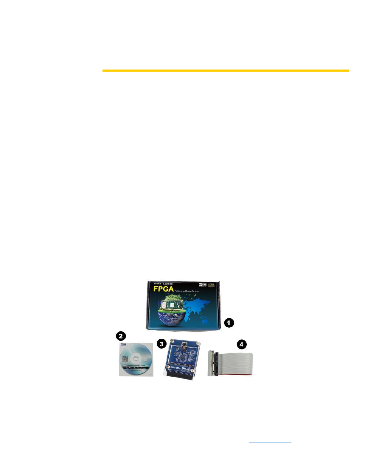
1.1 Package Contents
Figure 1-1 The D8M package contents
The D8M package includes:
⚫ Product Box
T
Page 5
5
Terasic Inc.
D8M-GPIO User Manual
www.terasic.com
September 26, 2018
⚫ System CD Download Guide
⚫ One D8M Module
⚫ 40-Pin IDC To Box Header Cable
1.2 D8M System CD
The D8M System CD contains all the documents and supporting materials associated
with D8M, including the user manual, reference designs, and device datasheets. Users
can download this system CD from the link: http://d8m.terasic.com/cd.
1.3 Assemble the Camera
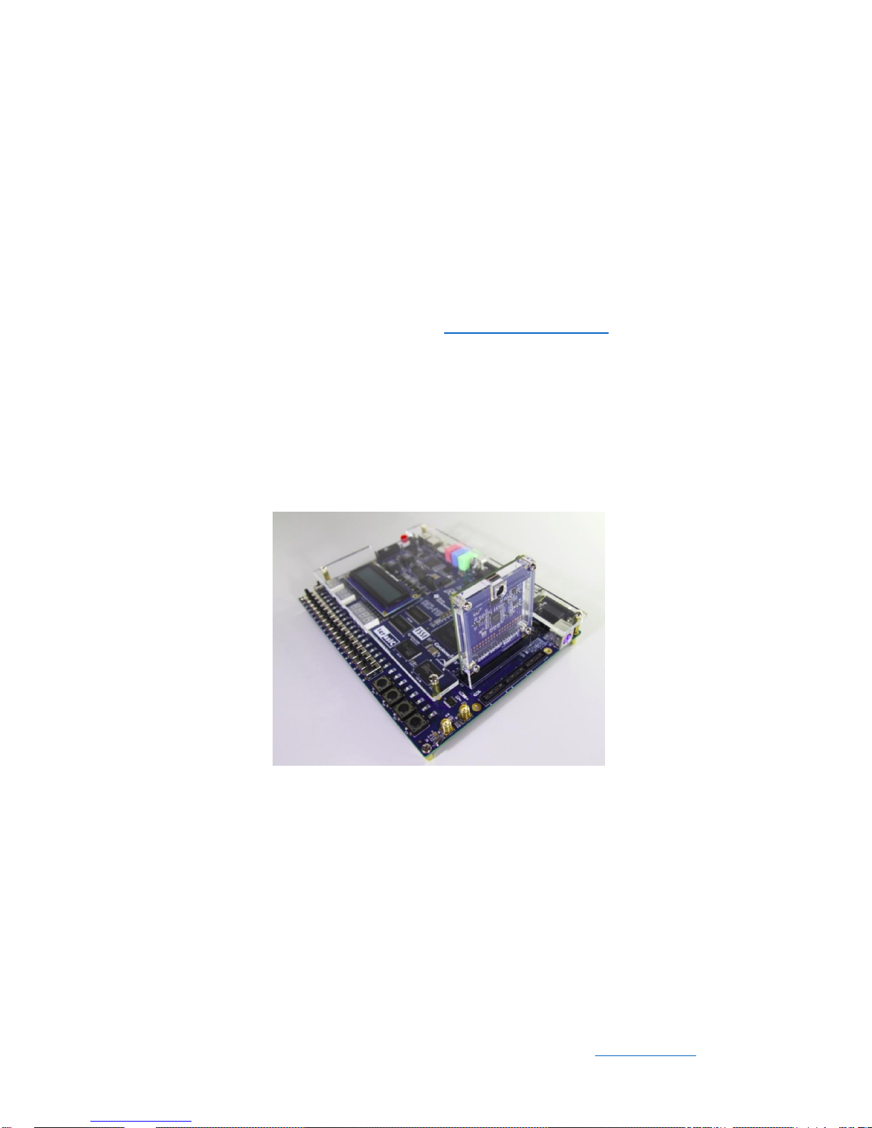
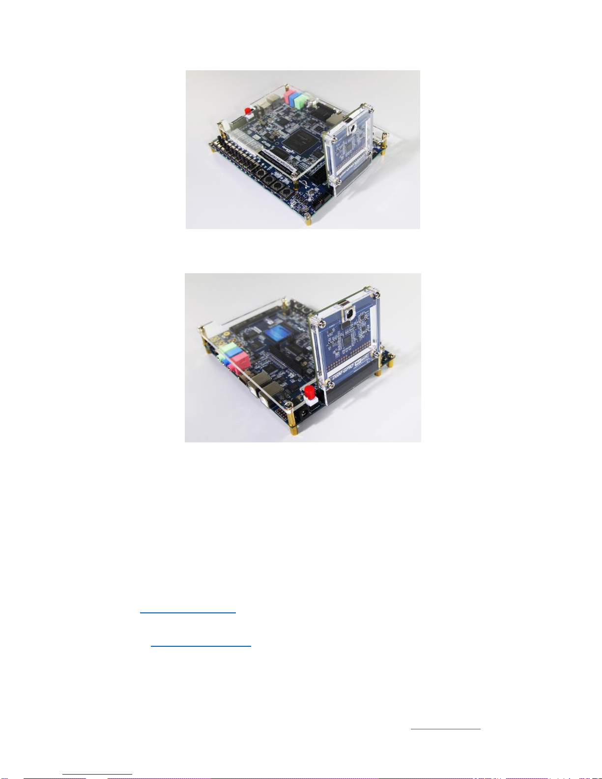
Terasic D8M is able to connect on to any FPGA development kit that is equiped with a
2x20 Pin GPIO connector. The pictures below show the connections allowing the D8M
to connect to 3 different Terasic FPGA Boards:
Figure 1-2 Connect the D8M to DE2-115 board’s expansion port
Page 6
6
Terasic Inc.
D8M-GPIO User Manual
www.terasic.com
September 26, 2018
Figure 1-3 Connect the D8M to DE1-SoC board’s expansion port
Figure 1-4 Connect the D8M to C5G board’s expansion port
1.4 Getting Help
Here are the addresses where you can get help if you encounter any problems:
Terasic Technologies
9F., No.176, Sec.2, Gongdao 5th Rd, East Dist, Hsinchu City, 30070. Taiwan
Email: support@terasic.com
Tel.: +886-3-575-0880
Website: http://d8m.terasic.com
Page 7
7
Terasic Inc.
D8M-GPIO User Manual
www.terasic.com
September 26, 2018
Chapter 2
Introduction of the
D8M Board
2.1 Features
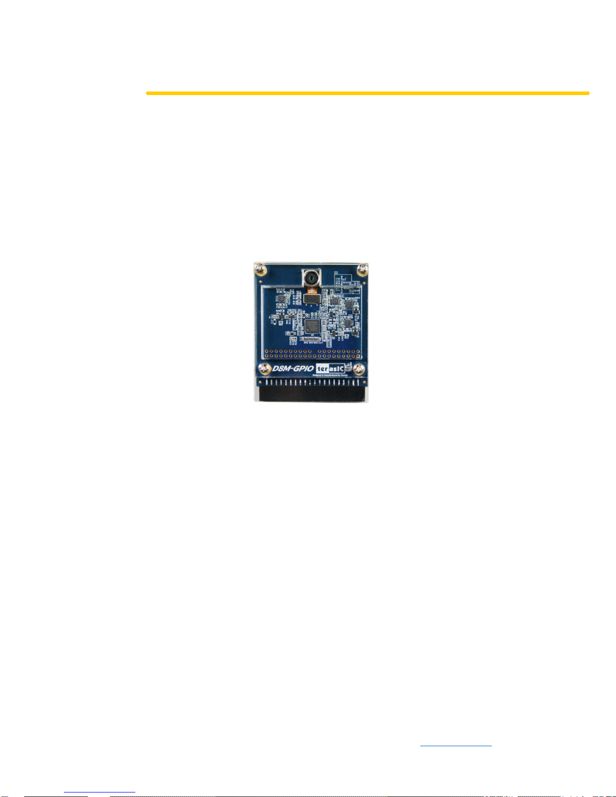
Figure 2 1 shows a photograph of the board.
Figure 2-1 shows a photograph of the board.
The D8M board has many features that allow users to implement a wide range of
designed circuits, from simple circuits to various multimedia projects.
The following hardware is provided on the board:
⚫ Package Interface:2x20 GPIO, 3.3V I/O-standard.
⚫ MIPI Camera Module:
◼ Chip P/N:OV8865
◼ Color Filter Arrangement:Bayer Pattern
◼ View Angel:70 °
◼ Pixels:3268x2448 (8-Mega Pixels)
◼ Frame Rate:8-Mega Pixels @30fps
◼ Support Focus Control
◼ Programmable controls for frame rate, mirror and flip, cropping, and
windowing
⚫ MIPI Decoder:
◼ Chip P/N:TC358748XBG
◼ MIPI CSI-2 Compliant
Page 8
8
Terasic Inc.
D8M-GPIO User Manual
www.terasic.com
September 26, 2018
◼ MIPI to Parallel Port Converter
◼ Supports up to 4 data lanes
◼ Package Size:73.4x60.0 mm
⚫ Package Size:73.4x60.0 mm
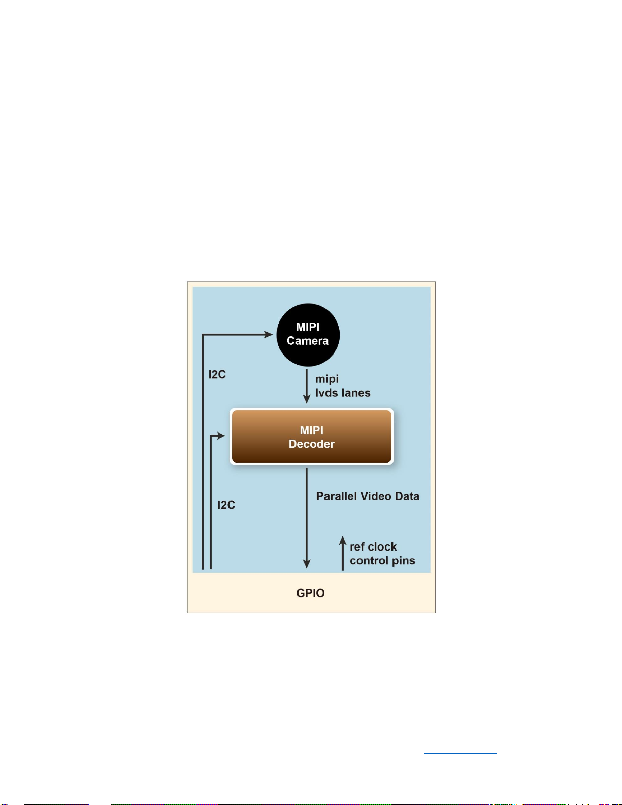
2.2 Block Diagram of the D8M Board
Below Figure 2-2 shows the D8M Block Diagram. MIPI Camera Module outputs 4
Lanes MIPI interface image data, which can be converted to Parallel data by passing
through the MIPI Decoder IC to the GPIO interface. Both MIPI Camera Module and
MIPI Decoder can be controlled by FPGA I2C interface.
Figure 2-2 Block diagram of D8M Board
Page 9
9
Terasic Inc.
D8M-GPIO User Manual
www.terasic.com
September 26, 2018
Chapter 3
Using the D8M Board
his chapter provides instructions on how to use the MIPI camera module, MIPI
Decoder and GPIO connector on the D8M board.
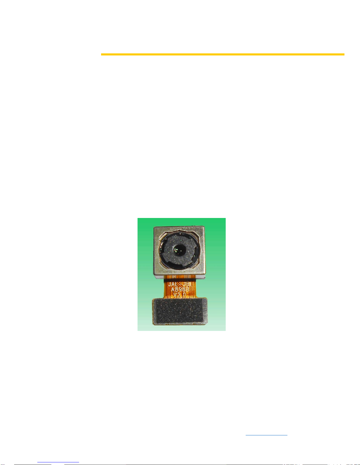
3.1 MIPI Camera Module
Terasic D8M board equips with an 8M pixel MIPI camera module named OV8865 (See
Figure 3-1). The OV8865 color image sensor is a high performance, 8 megapixel RAW
image sensor that delivers 3264x2448. It provides options for multiple resolutions while
maintaining full field of view. Users can program image resolution, frame rate, and
image quality parameters. Camera functions are controlled via I2C bus
(CAMERA_I2C_SDA and CAMERA_I2C_SCL). The I2C device address is 0x6C.
Figure 3-1 MIPI Camera Module
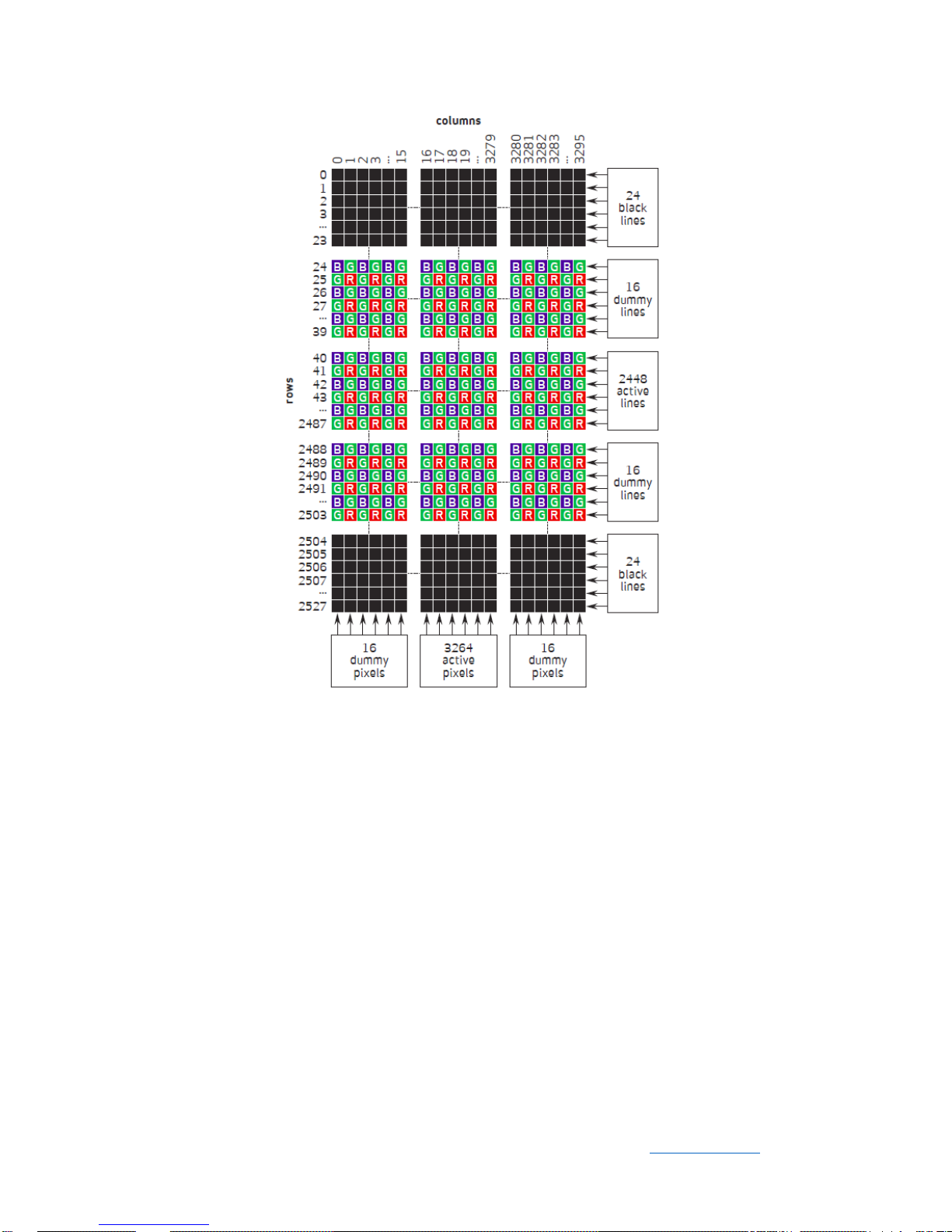
Figure 3-2 shows a cross-section of the image sensor array. The color filter is
arranged in a Bayer pattern. Of the 8,332,288 pixels, 7990,272 (3264x2448) are active
pixels and can be output. The other pixels are used for black level calibration and
interpolation.
T
Page 10
10
Terasic Inc.
D8M-GPIO User Manual
www.terasic.com
September 26, 2018
Figure 3-2 Sensor Array Region color filter Layout (From Camera Datasheet)
For more hardware description and register information about this camera module,
please refer to the datasheet named OV8865 Data Sheet.pdf in the D8M System CD.
In addition, there is a Voice Coil Motor (VCM) driver chip named VM149C on the MIPI
camera module. Users can use the same I2C bus (I2C device address is 0x18) to
modify the DAC value in the VCM driver chip that can allow the VCM to move its lens to
the desired position for getting a sharp image and realizing the Auto Focus (AF) feature.
Terasic also provides an AF demonstration and IP in the System CD. See section 4.x
for details. The datasheet of this VMC driver IC named VM149C VCM Driver IC.pdf
also can be found in the System CD.
Page 11
11
Terasic Inc.
D8M-GPIO User Manual
www.terasic.com
September 26, 2018
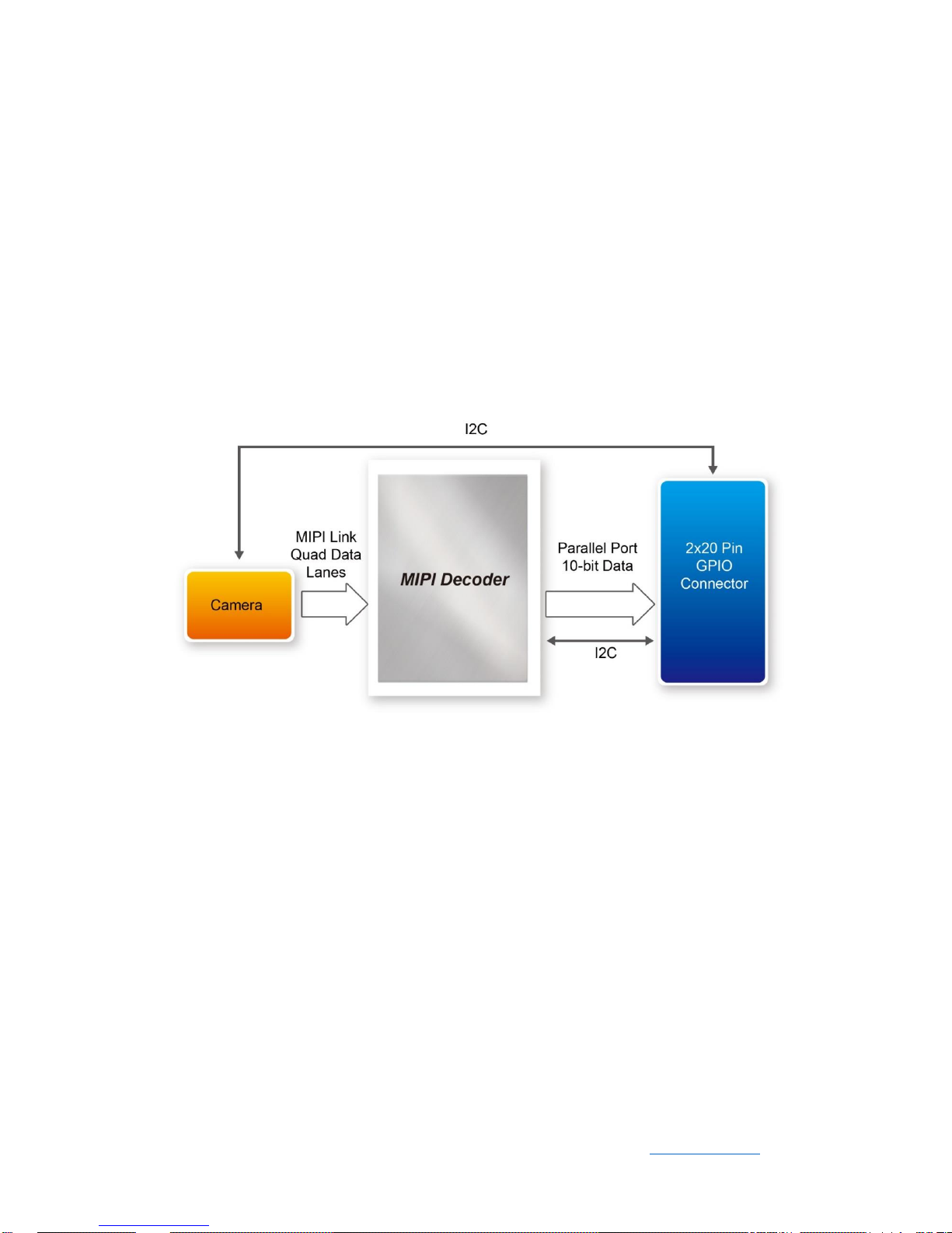
3.2 MIPI Decoder
The MIPI camera module output interface is MIPI interface, which cannot directly
connect to the Terasic FPGA board; therefore, a MIPI Decoder (TC358748XBG) is
added to convert MIPI interface to a parallel port interface (See Figure 3-3). Decoder
users can quickly obtain the image data and process it. MIPI Decoder can convert MIPI
Interface up to 24-bit data. The Camera module used on the D8M can only output 10
bit data, MIPI_PIXEL_D[9:0] the GPIO connector is the camera image output data bus,
and MIPI_PIXEL_D[13:10] is reserved for an alternative camera module with more
output bits.
Figure 3-3 System Overview with MIPI Decoder in CSI-2 RX to Parallel Port
Configuration
FPGA also can read/write MIPI Decoder through a I2C bus (MIPI_I2C_SDA /
MIPI_I2C_SCL ; I2C device address is 0x1C), which is different from the camera
module I2C bus. On the D8M board, MIPI Decoder can output clocks to the MIPI
camera and FPGA board. So in the demonstrations, most of them show how to control
IC PLL parameters as well as others. You can refer to section 3-4 clock tree for details.
Page 12
12
Terasic Inc.
D8M-GPIO User Manual
www.terasic.com
September 26, 2018
3.3 GPIO Connector
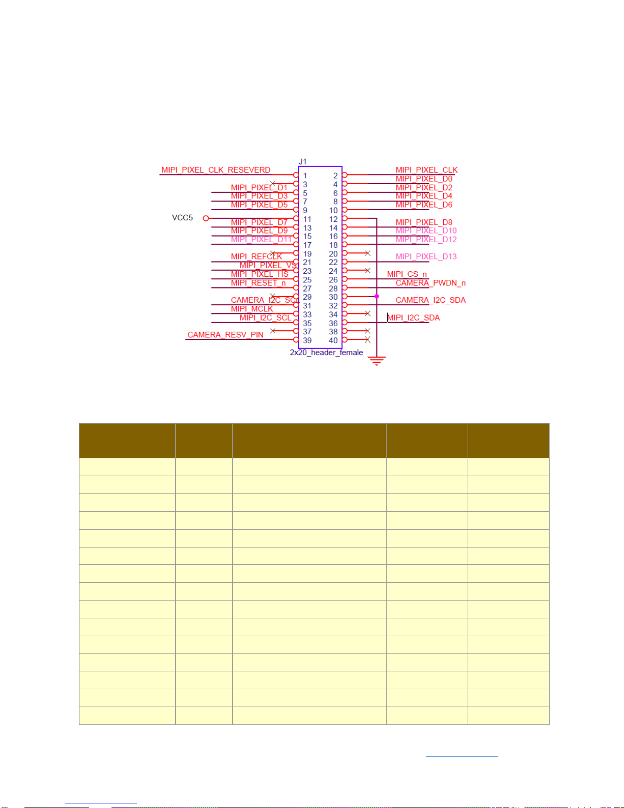
Figure 3-4 and Table 3-1 shows the pin out and pin definitions of the GPIO connector.
Figure 3-4 Pin-out of the 40-pin connector on D8M
Table 3-1 Pin Assignment of D8M GPIO Interface
Signal Name
Connector
Pin No.
Description
Pin Direction
I/O Standard
MIPI_PIXEL_D[0]
4
Parallel Port Data
Output
3.3V
MIPI_PIXEL_D[1]
5
Parallel Port Data
Output
3.3V
MIPI_PIXEL_D[2]
6
Parallel Port Data
Output
3.3V
MIPI_PIXEL_D[3]
7
Parallel Port Data
Output
3.3V
MIPI_PIXEL_D[4]
8
Parallel Port Data
Output
3.3V
MIPI_PIXEL_D[5]
9
Parallel Port Data
Output
3.3V
MIPI_PIXEL_D[6]
10
Parallel Port Data
Output
3.3V
MIPI_PIXEL_D[7]
13
Parallel Port Data
Output
3.3V
MIPI_PIXEL_D[8]
14
Parallel Port Data
Output
3.3V
MIPI_PIXEL_D[9]
15
Parallel Port Data
Output
3.3V
MIPI_PIXEL_D[10]
16
Reserve
Output
3.3V
MIPI_PIXEL_D[11]
17
Reserve
Output
3.3V
MIPI_PIXEL_D[12]
18
Reserve
Output
3.3V
MIPI_PIXEL_D[13]
22
Reserve
Output
3.3V
MIPI_RESET_n
27
Master Reset signal for MIPI
Input
3.3V
Page 13

13
Terasic Inc.
D8M-GPIO User Manual
www.terasic.com
September 26, 2018
camera and bridge device
MIPI_PIXEL_CLK
2
Parallel Port Clock signal
Output
3.3V
MIPI_PIXEL_HS
25
Parallel Port Horizontal
Synchronization signal
Output
3.3V
MIPI_PIXEL_VS
23
Parallel Port Vertical
Synchronization signal
Output
3.3V
MIPI_CS_n
26
Chip Select
Input
3.3V
MIPI_REFCLK
21
Reference Clock Input of bridge
device
Input
3.3V
MIPI_I2C_SCL
35
I2C Clock for bridge device
Input
3.3V
MIPI_I2C_SDA
36
I2C Data for bridge device
Inout
3.3V
CAMERA_PWDN_
n
28
Power Down signal of MIPI
camera
Input
3.3V
CAMERA_I2C_SCL
31
I2C Clock for MIPI camera
Input
3.3V
CAMERA_I2C_SD
A
32
I2C Data for MIPI camera
Inout
3.3V
VCC5
11
5V Power Input
N/A
N/A
GND
12 , 30
Ground
N/A
N/A
MIPI_PIXEL_CLK_
RESEVERD
1
Reserve
N/A
N/A
MIPI_MCLK
33
Reserve
N/A
N/A
CAMERA_RESV_P
IN
39
Reserve
N/A
N/A
Table3-2 shows the High/Low value of Input/Output Voltage Level on D8M GPIO digital
Interface.
Table 3-2 DC Electrical Specification
Parameter
Symbol
Min.
Max.
Unit
Input voltage, High level input
VIH
2.31
3.3
V
Input voltage, Low level input
VIL
0
0.99
V
Output voltage High level
VOH
2.64
3.3
V
Output voltage Low level
VOL 0 0.66
V
Page 14

14
Terasic Inc.
D8M-GPIO User Manual
www.terasic.com
September 26, 2018
3.4 Clock Tree
Figure 3-5 is the D8M board clock tree block diagram. MIPI Decoder PLL receives
FPGA Reference Clock (MIPI_REFCLK) and outputs Clock to Camera sensor (MCLK),
at the same time, MIPI Decoder PLL will also output a parallel port clock
(MIPI_PIXEL_CLK) and feedback to the FPGA to deal with parallel data.
Figure 3-5 Simple Clock Tree of the D8M Board
In the provided demonstrations, MIPI_REFCLK is set to 20MHz, FPGA transmits this
clock to the D8M MIPI Decoder PLL through the GPIO connector. No matter how much
the camera resolution is, the MCLK fixed output is 25MHz. According to the output
resolution, MIPI_PIXEL_CLK can be set as 25MHz for 640x480@60fps and 50MHz for
1920x1080@15fps.
For more MIPI Decoder PLL setting details, please refer to
TC358746AXBG_748XBG_rev09.pdf "Chapter 5: Clock and System" or refer to
Terasic demonstrations.
3.5 Camera Configuration
The developers should configure the camera OV8865 via I2C so the camera can
output desired image format. To get a better image quality, the following register
settings are strongly recommended. These settings are all applied in the CD demo
code. For detail information about the registers, please refer the OV8865 datasheet
included in the System CD.
Page 15

15
Terasic Inc.
D8M-GPIO User Manual
www.terasic.com
September 26, 2018
Register
Address
Register
Value
Description
0x4011
0x30
Enable the entering of a BLC (black level
calibration) offset.
0x4013
0xCF
BLC offset value.
0x3508
0x03
Increase the analog gain a bit to compensate for
the BLC offset.
0x5000
0x16
Turn off the LENC (lens correction)
compensation. This setting creates a very even
light distribution across the screen.
Page 16

16
Terasic Inc.
D8M-GPIO User Manual
www.terasic.com
September 26, 2018
Chapter 4
RTL Example Codes
This chapter provides instructions on how to capture a D8M image (resolution is
640X480@60 Hz) and use two storage methods (Line-Buffer and Frame-Buffer) to
display the image on a VGA Monitor. These storage methods realized by pure Verilog
HDL language have been validated on both DE1-SoC and DE2-115 board.
4.1 Using LINE- BUFFER
If the D8M resolution is set to 640x480@60Hz to output to VGA, as both image
capturing frequency and VGA output frequency are 60Hz, there is no need to use
Frame-Buffer to convert the frame rate, just adjust the frequency difference of the
Line-Buffer D8M pixel clock and VGA pixel clock. This demo mainly uses three
separate Line Buffers to do the frequency difference adjustment, at the same time, Line
Buffer are also used to store the data of converting image from RAW data to RGB data.
◼ Function Block Diagram
Figure 4-1 is the function block diagram of this demonstration. This demo uses three
Line-Buffers to store D8M 640x480@60 Hz raw data, and then extract two of the
Line-Buffers raw data to convert it to RGB data and output it to VGA with 640x480@60
Hz timing. This is how VGA Monitor can display the D8M capturing image. In this block,
it also provides an “auto-focusing” module, “monitor D8M frame rate” module, as well
as a pixel clock module. All module functions are described below:
⚫ MIPI_BRIDGE_CAMERA_Config: the D8M I2C setting controller, such as set
D8M to output 640X480@60Hz timing. It mainly writes I2C corresponding
parameters to D8M MIPI decoder IC register and Camera Sensor IC register
respectively through their own I2C buses. MIPI_I2C bus is used to write MIPI
decoder IC (I2C Slave Address = 0x1c.), CAMERA_I2C bus is used to write
Camera Sensor (IC Slave Address = 0x6c).
Page 17

17
Terasic Inc.
D8M-GPIO User Manual
www.terasic.com
September 26, 2018
Figure 4-1 Block diagram of the digital camera D8M design with Line -Buffer
⚫ D8M_SET: This module is used to process D8M 640X480@60Hz raw data. It
includes three Line-Buffers that are used to store raw data, and two of the
Line-Buffers raw data will be extracted and converted to RGB data, the
Line-Buffer is also used to adjust the frequency difference between D8M and VGA.
⚫ VGA_Controller_trig: the VGA signal timing generator, can generate 640x480@60
Hz signal timing.
⚫ FOCUS_ADJ: This module provides two main functions. The first function is using
I2C bus to write D8M Voice Coil Motor (VCM) driver IC register, and control the
camera lens’ movements to perform image focusing. VCM driver IC register (I2C
Slave Address =0x18) shares I2C bus with camera module. The other function is
doing the current image high frequency component statistic. When the VCM
drives the camera lens’ movement, a real-time statistics of image high-frequency
sum will be done in every step of the moving. Finally, the lens will move to a
position which has the largest number of high frequency to complete the
automatic focus operation. Focus area can be selected by SW3. There are two
options:
o Select focusing the whole screen area (set SW3 to 0)
o Select focusing the middle area (set SW3 to 1).
Once you set SW3 to a value (0 or 1) and press KEY3 one time, the automatic focus
operation will be performed in the selected area.
⚫ FpsMonitor: This module will count D8M MIPI_PIXEL_VS signal pulses in 1
Page 18

18
Terasic Inc.
D8M-GPIO User Manual
www.terasic.com
September 26, 2018
second (it stands fps number) and convert the number to a decimal number to
display on two seven-section LEDs.
⚫ CLOCKMEM: This module will divide the three clocks (VGA_CLK, MIPI_REFCLK
and MIPI_PIXEL_CLK) to 1Hz to display on LEDs. Users can observe the LEDs
to see if the clocks work or not.
We provide the Line-Buffer demonstrations on both DE1-SoC and DE2-115. The
switch setting and Key operation are the same on both DE1-SoC and DE2-115.
The following are the descriptions of the two platforms’ set up, as well as the test
steps.
DE1-SoC Demonstration:
◼ Hardware Setting Up
As shown in Figure 4-2
Figure 4-2 DE1-SoC demo hardware setting up
◼ Design Tools
⚫ Quartus II v15.0
◼ Demonstration Source Code
⚫ Quartus project directory: DE1_SOC_D8M_LB_RTL
⚫ Nios II Eclipse project workspace: DE1_SOC_D8M_LB_RTL.sof
Page 19

19
Terasic Inc.
D8M-GPIO User Manual
www.terasic.com
September 26, 2018
◼ Demonstration Batch File
⚫ Demo batch file folder: demonstrations\ DE1_SOC_D8M_LB_RTL\demo_batch
◼ Demonstration Setup
⚫ Connect the DE1-SoC board (J13) to the host PC with a USB cable and install the
USB-Blaster II driver if necessary.
⚫ Plug D8M onto DE1-SoC JP2(GPIO 1), connect VGA monitor to J9 see Figure
4-2.
⚫ Plug the 12V adapter to DE1-SoC Board.
⚫ Power on the DE1-SOC board.
⚫ Execute the demo batch file “test.bat” from the directory\
DE1_SOC_D8M_LB_RTL\demo_batch.
⚫ LED0~1 light up, stand the settings of D8M MIPI decoder IC and Camera Sensor
I2C are completed.
⚫ LED7~9 blink in 1Hz, stand VGA_CLK, MIPI_REFCLK and MIPI_PIXEL_CLK are
generated correctly.
⚫ HEX1~0 decimal number “60” stands D8M camera sensor capturing frame rate is
60Hz.
⚫ D8M capturing image displays on VGA monitor, if the VGA monitor image is fuzzy,
please press Key3 one time again (will perform the focus operation again). Users
can switch SW3 to “1” (there will be a yellow box on image), then, press KEY3 one
time again, the middle area focus operation will be performed.
Table 4-1 summarizes the functional keys and details of each LED status.
Table 4-1 The functional keys of the digital camera demonstration
Name
Description
LED0
Lights up when MIPI DECODER I2C setting is successful
LED1
Lights up when CAMERA I2C setting is successful
LED7
Blink in 1HZ ( VGA CLOCK/25M )
LED8
Blink in 1HZ (D8M REF CLOCK / 20M)
LED9
Blink in 1HZ (D8M PIXE CLOCK /50M)
HEX1-0
Display FRAME RATE in two decimal number
KEY0
SYSTEM RESET
KEY3
Image auto focus(area based on SW3 selection)
SW3
0: No yellow box (focus on whole screen area)
1: There is a yellow box(focus on yellow box)
Page 20
20
Terasic Inc.
D8M-GPIO User Manual
www.terasic.com
September 26, 2018
DE2-115 Demonstration:
◼ Hardware Setting Up
As shown in Figure 4-3
Figure 4-3 DE2-115 demo hardware setting up
◼ Design Tools
⚫ Quartus II v15.0
◼ Demonstration Source Code
⚫ Quartus project directory: DE2_115_D8M_LB_RTL
⚫ Nios II Eclipse project workspace: DE2_115_D8M_LB_RTL.sof
◼ Demonstration Batch File
⚫ Demo batch file folder: Demonstrations\ DE2_115_D8M_LB_RTL \demo_batch
◼ Demonstration Setup
⚫ Connect the DE2-115 board (J9) to the host PC with a USB cable and install the
USB-Blaster II driver if necessary.
⚫ Plug D8M onto DE2-115 JP5 (GPIO), connect VGA monitor to J13 (VGA) see
Figure 4-3.
⚫ Plug the 12V adapter to DE2-115 Board.
Page 21

21
Terasic Inc.
D8M-GPIO User Manual
www.terasic.com
September 26, 2018
⚫ Power on the DE2-115 board.
⚫ Execute the demo batch file “test.bat” from the directory\
DE2_115_D8M_LB_RTL\demo_batch.
⚫ LED0~1 light up, stand the settings of D8M MIPI decoder IC and Camera Sensor
I2C are completed.
⚫ LED7~9 blink in 1Hz, stand VGA_CLK, MIPI_REFCLK and MIPI_PIXEL_CLK are
generated correctly.
⚫ HEX1~0 decimal number “60” stands D8M camera sensor capturing frame rate is
60Hz.
⚫ D8M capturing image displays on VGA monitor, if the VGA monitor image is fuzzy,
please press Key3 one time again (will perform the focus operation again). Users
can switch SW3 to “1” (there will be a yellow box on image), then, press SW3 one
time again, the middle area focus operation will be performed.
Table 4-2 summarizes the functional keys and details of each LED status
Table 4-2 The functional keys of the digital camera demonstration
Name
Description
LED0
Lights up when MIPI DECODER I2C setting is successful
LED1
Lights up when CAMERA I2C setting is successful
LED7
Blink in 1HZ ( VGA CLOCK/25M )
LED8
Blink in 1HZ (D8M REF CLOCK / 20M)
LED9
Blink in 1HZ (D8M PIXE CLOCK /50M)
HEX1-0
Display FRAME RATE in two decimal number
KEY0
SYSTEM RESET
KEY3
Image auto focus(area based on SW3 selection)
SW3
0: No yellow box (focus on whole screen area)
1: There is a yellow box(focus on yellow box)
4.2 Using FRAME - BUFFER
This section provides instructions on how to store D8M capturing image(640x480@60
Hz)in a larger memory(Frame-Buffer, this Memory is expected to store up to one
Frame image), and how to extract Frame-Buffer address data to convert RAW data to
VGA data, and output the VGA data to VGA monitor with 640x480@60 Hz VGA timing.
◼ Function Block Diagram
Page 22

22
Terasic Inc.
D8M-GPIO User Manual
www.terasic.com
September 26, 2018
Figure 4-4 is the function block diagram of this demonstration. This design block is
similar to Line-Buffer’s. The only difference is one more Sdram_Control module is
there. This module can control general external SDRAM Memory and read/write image
data. As shown in the block diagram, D8M raw data will be written in SDRAM first. After
finishing writing a Frame, Sdram_Control module will read out the data from SDRAM to
RAW2RGB_J module to convert RAW data to RGB data. The RGB data will output
along with the signal timing generated by VGA_Controller to VGA monitor.
In the block, other module (for example, FOCUS_ADJ,
MIPI_BRIDGE_CAMERA_Config, FpsMonitor, CLOCKMEM) function instructions and
KEY/SW operations are the same with Line-Buffer’s:
Figure 4-4 Block diagram of the digital camera D8M design with Frame -Buffer
We provide the Frame-Buffer demonstrations on both DE1-SoC and DE2-115. And the
display resolution is 640x480@60Hz too. The demonstration setting up methods are
the same with section 4.1.Please see following instructions for details.
DE1-SoC Demonstration:
◼ Design Tools
⚫ Quartus II v15.0
◼ Demonstration Source Code
Page 23

23
Terasic Inc.
D8M-GPIO User Manual
www.terasic.com
September 26, 2018
⚫ Quartus project directory: Project directory: DE1_SOC_D8M_RTL
⚫ Nios II Eclipse project workspace: Bitstream used: DE1_SOC_D8M_RTL.sof
◼ Demonstration Batch File
⚫ Demo batch file folder: demonstrations\ DE1_SOC_D8M_RTL \demo_batch
◼ Demonstration Setup
⚫ Connect the DE1-SoC board (J13) to the host PC with a USB cable and
install the USB-Blaster II driver if necessary.
⚫ Plug D8M onto DE1-SoC JP2 (GPIO 1), connect VGA monitor to J9 see
Figure 4-2.
⚫ Plug the 12V adapter to DE1-SoC Board.
⚫ Power on the DE1-SOC board.
⚫ Execute the demo batch file “test.bat” from the directory\
DE1_SOC_D8M_RTL\demo_batch.
⚫ Below operations are the same with section 4.1 DE1_SoC Line-Buffer Demo.
DE2-115 Demonstration:
◼ Design Tools
⚫ Quartus II v15.0
◼ Demonstration Source Code
⚫ Quartus project directory: DE2_115_D8M_RTL
⚫ Nios II Eclipse project workspace: DE2_115_D8M_RTL.sof
◼ Demonstration Batch File
⚫ Demo batch file folder: Demonstrations\ DE2_115_D8M_RTL \demo_batch
◼ Demonstration Setup
⚫ Connect the DE2-115 board (J9) to the host PC with a USB cable and install
the USB-Blaster II driver if necessary.
⚫ Plug D8M onto DE2-115 JP5 (GPIO), connect VGA monitor to J13 (VGA) see
Figure 4 3.
⚫ Plug the 12V adapter to DE2-115 Board.
⚫ Power on the DE2-115 board.
⚫ Execute the demo batch file “test.bat” from the directory\
DE2_115_D8M_RTL\demo_batch.
⚫ Below operations are the same with section 4.1 DE2_115 Line-Buffer Dem
Page 24

24
Terasic Inc.
D8M-GPIO User Manual
www.terasic.com
September 26, 2018
Chapter 5
NIOS Based Example
Codes
his chapter provides several NIOS based examples for users to get started using the
D8M board.
5.1 DE1_SOC and DE2-115 D8M_VIP
Demonstration
This demonstration shows how to implement a D8M on DE1-SoC and DE2-115 Boards.
The Altera VIP (Video Image Processing) suite is used to display image/s on the VGA
monitor. The Nios II processor is used to configure the I2C devices. There is a Camera
IP from Terasic in Qsys, which translates the Bayer pattern from the camera to the
RGB video steam format and feeds it to the Altera VIP. The other IP developed by
Terasic for auto-focus is used to find the optimized focus settings of the user-defined
image area.
◼ Function Block Diagram
DE1_SOC_D8M_VIP reference design is developed based on Altera’s Video and
Image Processing (VIP) suite. The Terasic Camera IP translates the parallel Bayer
pattern data into RGB data to meet the specification of the Altera VIP video streaming.
The Frame Buffer from VIP is used for buffering image data in DDR3 and matching the
frame rate from the Terasic camera IP to the Clock Video Output of VIP. It displays the
final 640x480 RGB frame image on the VGA Monitor. The auto-focus IP by Terasic can
be used to get a better image quality by finding the optimized focus setting.
Figure 5-1 shows the Function block diagram of DE1_SOC_D8M_VIP demonstration.
T
Page 25

25
Terasic Inc.
D8M-GPIO User Manual
www.terasic.com
September 26, 2018
Figure 5-1 Function block diagram of DE1_SOC_D8M_VIP demonstration
The Nios II program running the on-chip memory controls the I2C controllers to
configure the image sensor, motor driver, and the MIPI Decoder IC. The first I2C
controller is used to configure the camera module, including the OV8865 image sensor
and the VM149C. The second I2C controller is used to configure the MIPI Decoder
TC358748XBG.
Note: The focus driver IC (VM149C) in the camera module is also configured by the
Terasic auto-focus IP through its own I2C master controller. Users must make sure
there is only one I2C master used one at a time.
◼ The default camera settings
In this demonstration, the default camera settings are:
⚫ Resolution: 600x480
⚫ Frame Rate: 60 fps
⚫ Pixel Data: RAW10
⚫ Bin Mode: 1, 2, 4 (achieved ZOOM-IN/ ZOOM-OUT function)
Users can change the settings base on their requirements.
◼ Design Tools
Page 26

26
Terasic Inc.
D8M-GPIO User Manual
www.terasic.com
September 26, 2018
⚫ Quartus II v15.0
⚫ Nios II Eclipse 15.0
◼ Demonstration Source Code
⚫ Quartus project directory: DE1_SOC_D8M_VIP
⚫ Nios II Eclipse project workspace: DE1_SOC_D8M_VIP\software
◼ Demonstration Batch File
⚫ Demo batch file folder: demonstrations\DE1_SOC_D8M_VIP\demo_batch
◼ Demonstration Setup
⚫ Connect a USB cable between the host PC and the USB connector (J13) on the
DE1-SOC board (See Figure 5-2).
⚫ Connect D8M module to GPIO1 (JP2) on DE1-SOC board.
⚫ Connect the VGA output of the DE1-SOC board to a VGA monitor.
⚫ Power on the DE1-SOC board.
⚫ Execute the demo batch file “test.bat” under the batch file folder
DE1_SOC_D8M_VIP\demo_batch.
⚫ The VGA Monitor will start showing the video captured from the camera.
⚫ Press KEY0 to trigger the auto-focus function.
⚫ Press KEY1/2 to trigger the manual focus adjustment.
⚫ Press KEY3 to trigger the ZOOM function.
⚫ Table 5-1 summarizes the functional keys.
Figure 5-2 Setup Connection of DE1_SOC_D8M_VIP demonstration
Page 27

27
Terasic Inc.
D8M-GPIO User Manual
www.terasic.com
September 26, 2018
Table 5-1 The functional keys of the digital camera demonstration
Component
Function Description
KEY0
Trigger AutoFocus
KEY1
Trigger Manual focus -
KEY2
Trigger Manual focus +
KEY3
Trigger ZOOM function
HEX[1:0]
fps (frames per sencond)
◼ Demonstration Setup for DE2-115 board
Users can also use the same Qsys and Altera VIP framework on the D8M and the
DE2-115 boards. Please refer to Figure 5-3 for hardware setup. The set up steps are
described below:
Figure 5-3 DE2-115 demo hardware setting up
⚫ Connect the DE2-115 board (J9) to the host PC with a USB cable and install the
USB-Blaster II driver if necessary.
⚫ Plug the D8M onto the DE2-115 JP5 (GPIO), and connect the VGA monitor to J13
(VGA).
Page 28

28
Terasic Inc.
D8M-GPIO User Manual
www.terasic.com
September 26, 2018
⚫ Plug the 12V adapter to the DE2-115 Board.
⚫ Power on the DE2-115 board.
⚫ Execute the demo batch file “DE2_115_D8M.bat” under the batch file folder
DE2_115_D8M_VIP\demo_batch.
⚫ Press KEY0 to trigger autofocus function.
⚫ Press KEY1/2 to trigger manual focus adjustment.
⚫ Press KEY3 to trigger ZOOM function.
Table 5-1 summarizes the functional keys.
5.2 DE1_SOC_D8Mx2_VIP Demonstration
This demonstration shows how to implement two D8M boards in DE1-SoC. Two D8M
streaming processed and mixed by the Altera VIP (Video Image Processing) suite and
finally displays images on the VGA monitor.
◼ Function Block Diagram
Figure 5-4 shows the Function block diagram of DE1_SOC_D8MX2_VIP
demonstration.
Page 29

29
Terasic Inc.
D8M-GPIO User Manual
www.terasic.com
September 26, 2018
Figure 5-4 Function block diagram of DE1_SOC_D8MX2_VIP demonstration
DE1_SOC_D8MX2_VIP reference design is developed based on Altera’s Video and
Image Processing (VIP) suite. This demo implements two D8M boards and outputs
their parallel images data into the FPGA. Insside the FPGA, image data will enter the
Terasic Camera IP, Cliper, Terasic AutoFocus and Scaller blocks sequentially. After that,
10bit RAW data will be converted to 24-bit RGB data (in 640x480 resolution) and
stored into the SDRAM as a cache via the Frame Buffer block. Then, these two image
streams will be read and blended together (in 800x600 resolution) by Mixer IP. Finally it
displays on the VGA monitor via Clock Video Output block.
The Nios II program running the on-chip memory controls on the two I2C controllers to
configure the image sensor, motor driver, and the MIPI CSI-2 Decoder IC.
Note: The focus driver IC (VM149C) in the camera module is also configured by the
Page 30

30
Terasic Inc.
D8M-GPIO User Manual
www.terasic.com
September 26, 2018
Terasic auto-focus IP through its own I2C master controller. Users must make sure
there is only one I2C master used a time.
◼ KEY IP Descriptions
In this demonstration, the default camera settings are:
⚫ Terasic Camera IP implements RAW to RGB and avalon-ST streaming
package conversion.
⚫ Terasic AutoFocus IP implements Simplified AutoFocus function.
⚫ Scaler IP implements Scaling function. Combining with software
configuration, it can scale two 640x480 images to proper size to fit the
bandwidth limitations (100MHz x 16bit) of the SDRAM.
⚫ Frame Buffer IP can read and write image stream into the SDRAM
⚫ Mixer IP Camera will blend two image data into one picture (resolution is
800x600).
⚫ Clock Video Output block will output the image data (resolution is 800x600)
from the Mixer IP to the VGA monitor.
◼ The default camera settings
In this demonstration, the default camera settings are:
⚫ Resolution: 600x480
⚫ Frame Rate: 50 fps
⚫ Pixel Data: RAW10
⚫ Bin Mode: 1, 2, 4 (achieved ZOOM-IN/ ZOOM-OUT function)
Camera1 default settings:
⚫ Resolution: 600x480
⚫ Frame Rate: 50 fps
⚫ Pixel Data: RAW10
⚫ Bin Mode: 1, 2, 4 (achieved ZOOM-IN/ ZOOM-OUT function)
Users can change the settings base on their requirements.
◼ Synchronize Two D8M Data Streaming
There is a simple way to synchronize multiple D8M’s “Frame Start” signals. See Table
5-2 follow the “Hardware standby with PWDNB” mode. After configuring all of the
D8M’s registers, just pulling all of the D8M’s “PWDNB” signal low for a while at the
same time. In this way, the register setting will not be clear and it will synchronize all
Page 31

31
Terasic Inc.
D8M-GPIO User Manual
www.terasic.com
September 26, 2018
the D8M’s “Frame Star”.
Table 5-2 Hardware and Standby Description
Mode
Description
Hardware standby with PWDNB
Enable by pulling PWDNB low
Input clock is gated by PWDNB, no SCCB
communication
Register value are maintained
Power down all blocks and regulator
Low power consumption
GPIO can be configured as high/low/tri-state
◼ Design Tools
⚫ Quartus II v15.0
⚫ Nios II Eclipse 15.0
◼ Demonstration Source Code
⚫ Quartus project directory: DE1_SOC_D8MX2_VIP
⚫ Nios II Eclipse project workspace: DE1_SOC_D8M_VIP\software
◼ Demonstration Batch File
⚫ Demo batch file folder: demonstrations\DE1_SOC_D8MX2_VIP\demo_batch
◼ Demonstration Setup
⚫ Connect a USB cable between the host PC and the USB connector (J13) on
the DE1-SOC board.
⚫ Connect the two D8M modules to GPIO0 (JP1) and GPIO1 (JP2) on
DE1-SOC board (See Figure 5-5).
⚫ Connect the VGA output of the DE1-SOC board to a VGA monitor.
Page 32

32
Terasic Inc.
D8M-GPIO User Manual
www.terasic.com
September 26, 2018
Figure 5-5 Function block diagram of DE1_SOC_D8MX2_VIP demonstration
⚫ Power on the DE1-SOC board.
⚫ Execute the demo batch file “test.bat” under the batch file folder
DE1_SOC_D8M_VIP\demo_batch.
⚫ The VGA Monitor will start showing the video captured from the camera.
⚫ Put SW1 to low position(Camera Function)
⚫ Press KEY0 to trigger autofocus function.
⚫ Press KEY1/2 to trigger manual focus adjustment.
⚫ Press KEY3 to trigger ZOOM function.
⚫ Note SW0 high to configure camera 1,SW0 low to configure camera 0
⚫ Put SW1 to high position (Mixer Function).
⚫ Press KEY0 to trigger display mode change as shown in Figure 5-6.
Figure 5-6 Four display modes in Mixer function.
⚫ Press KEY1/2 to scale camera video to left/right position (See Figure 5-7) or
upper left / lower right position (See Figure 5-8).
Page 33

33
Terasic Inc.
D8M-GPIO User Manual
www.terasic.com
September 26, 2018
Figure 5-7 Scale video size of camera0 or camera1 on left/right position
Figure 5-8 Scale video size of camera0 or camera1 in the upper left or lower right
position
⚫ Press KEY3 to trigger Stop/Run camera0 (SW0 in low position) or camera1 (SW0
in high position) function.
⚫ Note : Put SW0 to high position to configure camera1, put SW0 to low position to
configure camera0.
Table 5-3 summarizes the functional keys.
Page 34

34
Terasic Inc.
D8M-GPIO User Manual
www.terasic.com
September 26, 2018
Table 5-3 The functional keys of the digital camera demonstration
5.3 C5G_D8M_VIP Demonstration
This demonstration shows how to implement a camera demo in Altera Qsys tool. Altera
VIP (Video Image Processing) suite is used to display the image on the HDMI monitor
and the Nios II processor is used to configure the I2C devices. There is a Camera IP
from Terasic in Qsys, which translates the Bayer pattern from camera to the RGB video
steam format, and feeds it to Altera VIP. The other IP developed by Terasic for
auto-focus is used to find the optimized focus settings of user-defined image area.
◼ Function Block Diagram
Figure 5-9 shows the Function block diagram of C5G_D8M_VIP demonstration.
Component
Function Description
SW1 low: Camera
Function
SW1 high: Mixer Function
KEY0
Trigger AutoFocus
display mode change
KEY1
Trigger Manual focus -
Scale camera video to
right/bottom
KEY2
Trigger Manual focus +
Scale camera video to left/top
KEY3
Trigger ZOOM function
Stop/Run camera0/1
SW0
Camera configure select:
high: configure Camera 1
low : configure Camera 0
SW1
KEY0-3 function switch
HEX[1:0]
fps (frames per sencond)
Page 35

35
Terasic Inc.
D8M-GPIO User Manual
www.terasic.com
September 26, 2018
Figure 5-9 Function block diagram of C5G_D8M_VIP demonstration
C5G_D8M_VIP reference design is developed based on Altera’s Video and Image
Processing (VIP) suite. The Terasic Camera IP translates the parallel Bayer pattern
data into RGB data to meet the specification of the Altera VIP video streaming. The
Frame Buffer from the VIP is used for buffering image data in DDR3 and matching the
frame rate from the Terasic camera IP to the Clock Video Output of the VIP. It displays
the final 640x480 RGB frame image on the HDMI monitor. The auto-focus IP by Terasic
can be used to get a better image quality by finding the optimized focus setting.
The Nios II program running the on-chip memory controls the two I2C controllers to
configure the image sensor, motor driver, and the MIPI Decoder IC. The first I2C
controller is used to configure the camera module, including the OV8865 image sensor
and the VM149C. The second I2C controller is used to configure the MIPI Decoder
TC358748XBG.
Note: The focus driver IC (VM149C) in the camera module is also configured by the
Page 36

36
Terasic Inc.
D8M-GPIO User Manual
www.terasic.com
September 26, 2018
Terasic auto-focus IP through its own I2C master controller. Users must make sure
there is only one I2C master used at a time.
◼ The default camera settings
In this demonstration, the default camera settings are:
⚫ Resolution: 1920x1080
⚫ Frame Rate: 15 fps
⚫ Pixel Data: RAW10
⚫ Bin Mode: 1, 2, 4 (achieved ZOOM-IN/ ZOOM-OUT function)
Users can change the settings base on their requirements.
◼ Design Tools
⚫ Quartus II v15.0
⚫ Nios II Eclipse 15.0
◼ Demonstration Source Code
⚫ Quartus project directory: C5G_D8M_VIP
⚫ Nios II Eclipse project workspace: C5G_D8M_VIP\software
◼ Demonstration Batch File
⚫ Demo batch file folder: demonstrations\DE1_SOC_D8M_VIP\demo_batch
◼ Demonstration Setup
⚫ Switch the Dip Switch S1/S2 which is located on the back of the board to the
"OFF" position.
⚫ Connect a USB cable between the host PC and the USB connector (J10) on the
C5G board (See Figure 5-10).
⚫ Connect D8M module in GPIO0(JP9) on C5G board.
⚫ Connect the VGA output of the C5G board to a HDMI monitor.
⚫ Power on the C5G board.
⚫ Execute the demo batch file “test.bat” under the batch file folder
C5G_D8M_VIP\demo_batch.
⚫ The HDMI monitor will start showing the video captured from the camera.
⚫ Press KEY0 to trigger autofocus function.
⚫ Press KEY1/2 to trigger manual focus adjustment.
⚫ Table 5-4 summarizes the functional keys.
Page 37

37
Terasic Inc.
D8M-GPIO User Manual
www.terasic.com
September 26, 2018
Figure 5-10 Setup Connection of DE1_SOC_D8M_VIP demonstration
Table 5-4 The functional keys of the digital camera demonstration
Component
Function Description
KEY0
Trigger AutoFocus
KEY1
Trigger Manual focus -
KEY2
Trigger Manual focus +
KEY3
Trigger ZOOM function
HEX[1:0]
fps (frames per sencond)
Page 38

38
Terasic Inc.
D8M-GPIO User Manual
www.terasic.com
September 26, 2018
Chapter 6
Appendix
6.1 Revision History
Version
Change Log
V1.0
Initial Version
V1.0.1
Modify Figure 3-1
V1.0.2
Modify Support information and page21
V1.1.0
Add recommend register setting for camera
V1.1.1
Modify Figure 4-4
V1.1.2
Modify VCM149C to VM149C
6.2 Copyright Statement
Copyright © 2018 Terasic Inc. All rights reserved.
Page 39

Mouser Electronics
Authorized Distributor
Click to View Pricing, Inventory, Delivery & Lifecycle Information:
Terasic:
P0447
 Loading...