


Apollo Carrier Board
User Manual
1
www.terasic.com
May 8, 2020

Apollo Carrier Board
User Manual
1
www.terasic.com
May 8, 2020
CONTENTS
Chapter 1 Overview .......................................................................................................... 3
1.1 General Description ............................................................................................................................... 3
1.2 Key Features........................................................................................................................................... 4
1.3 Block Diagram ....................................................................................................................................... 4
Chapter 2 Board Components ......................................................................................... 5
2.1 Board Overview ..................................................................................................................................... 5
2.2 Power Input and Switch ......................................................................................................................... 5
2.3 General User Input and Output .............................................................................................................. 6
2.4 Clock Generator ................................................................................................................................... 11
2.5 QSFP28 Ports ....................................................................................................................................... 12
2.6 PCI Express .......................................................................................................................................... 14
2.7 USB Downstream Port ......................................................................................................................... 15
Chapter 3 Board Assembly ............................................................................................. 17
3.1 SAMTEC JOM..................................................................................................................................... 17
3.2 Assembly .............................................................................................................................................. 18
3.3 Disassembly ......................................................................................................................................... 20
Chapter 4 Setup Thunderbolt3 ...................................................................................... 23
4.1 Hardware Requirement ........................................................................................................................ 23
4.2 Thunderbolt 3 Test on Windows OS .................................................................................................... 24
4.3 Detect PCIe Device in the FPGA ......................................................................................................... 26
Chapter 5 PCI Express Reference Design for Windows .............................................. 28
5.1 PCI Express System Infrastructure ...................................................................................................... 28
5.2 PC PCI Express Software SDK ............................................................................................................ 29
5.3 PCI Express Software Stack ................................................................................................................. 29
5.4 PCI Express Library API ...................................................................................................................... 34
5.5 PCIe Reference Design - DDR4........................................................................................................... 39
Chapter 6 Transceiver Verification ................................................................................ 47

Apollo Carrier Board
User Manual
2
www.terasic.com
May 8, 2020
6.1 Transceiver Test Code .......................................................................................................................... 47
6.2 QSFP28 Ports ....................................................................................................................................... 47
6.3 40G Ethernet Example ......................................................................................................................... 48
Chapter 7 Additional Information................................................................................. 54
7.1 Getting Help ......................................................................................................................................... 54

Apollo Carrier Board
User Manual
3
www.terasic.com
May 8, 2020
T
Chapter 1
Overview
his chapter provides an overview of the Apollo Carrier board and installation guide.
1.1 General Description
Apollo Carrier board is a Carrier board design for Terasic Apollo S10 SoM board. Apollo Carrier
board and Apollo S10 SoM board communication via FMC and FMC+ connectors. Apollo Carrier
board provides 12V DC power for Apollo S10 via SAMTEC 2x6 connector.
Figure 1-1 Apollo S10 SoM and Carrier board

Apollo Carrier Board
User Manual
4
www.terasic.com
May 8, 2020
1.2 Key Features
The following hardware is implemented on the Apollo Carrier board:
Carrier board for Apollo S10 SoM
Power input: 12V DC via PCIe 2x4 power connector
Provides 12V DC to S10 via SAMTEC 2x6 power connector
Signals connect to S10 via FMC+(J1) and FMC connectors
PCIe Gen3 x4 via Thunderbolt 3 (Type-C connector)
USB Downstream port via Thunderbolt 3 (Type-A connector)
Two QSFP28 connectors (40G Ethernet)
Clock generator to provide reference clock for transceiver IP
LED x4, Button x2, Switch x2
2x20 3.3V GPIO expansion header
HDMI-TX Port. Not function now, reserved for future
1.3 Block Diagram
Figure 1-2 shows the block diagram of the Apollo Carrier board.
Figure 1-2 Block Diagram of the Apollo Carrier Board

Apollo Carrier Board
User Manual
5
www.terasic.com
May 8, 2020
T
Chapter 2
Board Components
his chapter introduces all the important components on the Apollo Carrier Board.
2.1 Board Overview
Figure 2-1 is the top view of the Apollo Carrier Board. It depicts the layout of the board and
indicates the location of the connectors and key components. Users can refer to this figure for
relative location of the connectors and key components.
2.2 Power Input and Switch
Figure 2-2 shows the 12V DC power input and power switch on the Carrier board. The 12V DC
power is input via 2x4 PCIe power connector.
Figure 2-1 Apollo Carrier Board (top view)

Apollo Carrier Board
User Manual
6
www.terasic.com
May 8, 2020
Figure 2-2 Position of 12V DC Input and Power Switch
After Apollo S10 and Apollo Carrier Board are assembled, please:
Always make Apollo S10 SoM power switch on.
Do not use the 2x4 PCIe power connector on Apollo S10.
2.3 General User Input and Output
This section describes the user I/O interface of the Carrier board.
User Defined Button/Switch/LED
There are two buttons, two switches, and four LEDs on the Carrier board, as shown in Figure 2-3.
Figure 2-3 User Button, Switch and LED

Apollo Carrier Board
User Manual
7
www.terasic.com
May 8, 2020
Schematic
Signal Name
Description
I/O Standard
FMC
Pin Num.
Apollo S10
FPGA Pin Num.
LED[0]
Driving logic 0 on the I/O port turns
the LED ON. Driving logic 1 on the
I/O port turns the LED OFF.
1.8 V
D17
PIN_E21
LED[1]
1.8 V
D18
PIN_D21
LED[2]
1.8 V
H19
PIN_G19
LED[3]
1.8 V
H20
PIN_F19
SW[0]
High logic level when SW in the
UPPER position.
1.8 V
D14
PIN_G20
SW[1]
1.8 V
D15
PIN_H20
KEY[0]
High Logic Level when the button is
not pressed
1.8 V
C14
PIN_J21
KEY[1]
1.8 V
C15
PIN_H21
Table 2-1 General User I/O Pin Assignments, Schematic Signal Names, and Functions
2x20 GPIO Header (Timing Expansion Header)
The board has one 2x20 GPIO headers. Each header has 36 user pins connected to the FMC
connector via voltage level translator (See Figure 2-4). The 2x20 GPIO I/ o standard can support
three I / O standards including 1.8, 2.5 and 3.3V. Users can select the desired voltage setting
through the JP2 header (See Figure 2-5 and Table 2-2). It also comes with DC +5V (VCC5), DC
+3.3V (VCC3P3), and two GND pins. Figure 2-6 and Figure 2-7 show the I/O distribution of the
GPIO connector. The maximum power consumption allowed for a daughter card connected to the
GPIO ports is shown in Table 2-3 and Table 2-4 shows all the pin assignments of the GPIO
connector. The pin-out of JP1 is shown in
Figure 2-4 Connection between 2x20 GPIO and Apollo S10 SoM

Apollo Carrier Board
User Manual
8
www.terasic.com
May 8, 2020
JP2 Setting
FMC I/O Standard
3.3V(Default Setting)
2.5V
Figure 2-5 Location of the JP2
Table 2-2 Header setting for I/O standard of the JP2

Apollo Carrier Board
User Manual
9
www.terasic.com
May 8, 2020
1.8V
Figure 2-6 Pin 1 of the GPIO header
Figure 2-7 Pin-out of 2x20 GPIO Header JP1

Apollo Carrier Board
User Manual
10
www.terasic.com
May 8, 2020
JP2 Setting
FMC I/O Standard
5V
1A (depend on the power adapter
specification.)
3.3V
1.5A
Schematic
Signal Name
Description
I/O Standard
FMC
Pin Num.
Apollo S10
FPGA Pin Num.
FMC_GPIO_D[0]
GPIO Connection[0]
3.3(Default)/2.5/1.8V
G6
PIN_J20
FMC_GPIO_D[1]
GPIO Connection[1]
3.3(Default)/2.5/1.8V
G33
PIN_C23
FMC_GPIO_D[2]
GPIO Connection[2]
3.3(Default)/2.5/1.8V
D8
PIN_E18
FMC_GPIO_D[3]
GPIO Connection[3]
3.3(Default)/2.5/1.8V
H32
PIN_G24
FMC_GPIO_D[4]
GPIO Connection[4]
3.3(Default)/2.5/1.8V
G34
PIN_B23
FMC_GPIO_D[5]
GPIO Connection[5]
3.3(Default)/2.5/1.8V
G31
PIN_H22
FMC_GPIO_D[6]
GPIO Connection[6]
3.3(Default)/2.5/1.8V
H31
PIN_F24
FMC_GPIO_D[7]
GPIO Connection[7]
3.3(Default)/2.5/1.8V
H29
PIN_J24
FMC_GPIO_D[8]
GPIO Connection[8]
3.3(Default)/2.5/1.8V
C27
PIN_K23
FMC_GPIO_D[9]
GPIO Connection[9]
3.3(Default)/2.5/1.8V
G28
PIN_R23
FMC_GPIO_D[10]
GPIO Connection[10]
3.3(Default)/2.5/1.8V
G30
PIN_G22
FMC_GPIO_D[11]
GPIO Connection[11]
3.3(Default)/2.5/1.8V
C26
PIN_J23
FMC_GPIO_D[12]
GPIO Connection[12]
3.3(Default)/2.5/1.8V
D27
PIN_F22
FMC_GPIO_D[13]
GPIO Connection[13]
3.3(Default)/2.5/1.8V
D26
PIN_E22
FMC_GPIO_D[14]
GPIO Connection[14]
3.3(Default)/2.5/1.8V
H28
PIN_K24
FMC_GPIO_D[15]
GPIO Connection[15]
3.3(Default)/2.5/1.8V
D24
PIN_A24
FMC_GPIO_D[16]
GPIO Connection[16]
3.3(Default)/2.5/1.8V
C23
PIN_C20
FMC_GPIO_D[17]
GPIO Connection[17]
3.3(Default)/2.5/1.8V
D23
PIN_B24
FMC_GPIO_D[18]
GPIO Connection[18]
3.3(Default)/2.5/1.8V
G15
PIN_A19
FMC_GPIO_D[19]
GPIO Connection[19]
3.3(Default)/2.5/1.8V
C22
PIN_D20
FMC_GPIO_D[20]
GPIO Connection[20]
3.3(Default)/2.5/1.8V
G18
PIN_F17
FMC_GPIO_D[21]
GPIO Connection[21]
3.3(Default)/2.5/1.8V
D21
PIN_C18
FMC_GPIO_D[22]
GPIO Connection[22]
3.3(Default)/2.5/1.8V
G19
PIN_E17
FMC_GPIO_D[23]
GPIO Connection[23]
3.3(Default)/2.5/1.8V
C19
PIN_F21
FMC_GPIO_D[24]
GPIO Connection[24]
3.3(Default)/2.5/1.8V
G21
PIN_B18
FMC_GPIO_D[25]
GPIO Connection[25]
3.3(Default)/2.5/1.8V
C18
PIN_F20
FMC_GPIO_D[26]
GPIO Connection[26]
3.3(Default)/2.5/1.8V
G22
PIN_B19
FMC_GPIO_D[27]
GPIO Connection[27]
3.3(Default)/2.5/1.8V
D20
PIN_C17
FMC_GPIO_D[28]
GPIO Connection[28]
3.3(Default)/2.5/1.8V
H22
PIN_A22
FMC_GPIO_D[29]
GPIO Connection[29]
3.3(Default)/2.5/1.8V
G27
PIN_P23
Table 2-3 Voltage and Max. Current Limit of GPIO Header
Table 2-4 2x20 GPIO Pin Assignments, Schematic Signal Names, and Functions

Apollo Carrier Board
User Manual
11
www.terasic.com
May 8, 2020
FMC_GPIO_D[30]
GPIO Connection[30]
3.3(Default)/2.5/1.8V
G24
PIN_A17
FMC_GPIO_D[31]
GPIO Connection[31]
3.3(Default)/2.5/1.8V
H26
PIN_A21
FMC_GPIO_D[32]
GPIO Connection[32]
3.3(Default)/2.5/1.8V
H23
PIN_B22
FMC_GPIO_D[33]
GPIO Connection[33]
3.3(Default)/2.5/1.8V
H25
PIN_A20
FMC_GPIO_D[34]
GPIO Connection[34]
3.3(Default)/2.5/1.8V
G16
PIN_B20
FMC_GPIO_D[35]
GPIO Connection[35]
3.3(Default)/2.5/1.8V
G25
PIN_B17
Schematic
Signal Name
Description
I/O Standard
Default Freq.
FMC
Pin Num.
Apollo S10
FPGA Pin Num.
FMCP_REFCLK_p
Reference clock FMC+
connector
LVDS
644.53125MHz
G6
PIN_AM41
QSFP28A_REFCLK_p
Reference clock for
QSFP28A
LVDS
644.53125MHz
G33
PIN_AM38
QSFP28B_REFCLK_p
Reference clock for
QSFP28B
LVDS
644.53125MHz
D8
PIN_T41
Si5340A_I2C_SCL
I2C clock bus of the
clock generator
1.8V
--
H32
PIN_AU34
Si5340A_I2C_SDA
I2C data bus of the
clock generator
1.8V
--
G34
PIN_AU33
SI5340A_OE_n
Enable output of the
clock generator
1.8V
--
G31
PIN_BG38
SI5340A_RST_n
Reset of the clock
1.8V
--
H31
PIN_BG37
2.4 Clock Generator
The Carrier board includes one Si5340A clock generator to provide reference clock for FPGA
transceiver IP as shown in Figure 2-8. To enable the clock generator, developers must well control
the control pins Si5340A_OE_n and Si5340A_RST_n on the Si5340A.
Figure 2-8 Si5340A of the Carrier Board
Table 2-5 Clock Generator Pin Assignments, Schematic Signal Names, and Functions

Apollo Carrier Board
User Manual
12
www.terasic.com
May 8, 2020
generator
Schematic
Signal Name
Description
I/O Standard
FMC
Pin Num.
Apollo S10
FPGA Pin Num.
QSFP28A_INTERRUPT_
Interrupt
1.8 V
H32
PIN_BF3
QSFP28A_LP_MODE
Low Power Mode
1.8 V
H31
PIN_BG3
QSFP28A_MOD_PRS_n
Module Present
1.8 V
G30
PIN_BC3
QSFP28A_MOD_SEL_n
Module Select
1.8 V
H28
PIN_BF3
QSFP28A_RST_n
Module Reset
1.8 V
H29
PIN_BF3
QSFP28A_SCL
2-wire serial interface clock
1.8 V
D26
PIN_BD3
QSFP28A_SDA
2-wire serial interface data
1.8 V
D27
PIN_BD3
QSFP28A_REFCLK_p
QSFP28A transceiver reference
clock p
LVDS
L8
PIN_AM3
QSFP28A_RX_p[0]
Receiver data of channel 0
HSSI
DIFFERENTIAL I/O
Z32
PIN_AL4
QSFP28A_RX_p[1]
Receiver data of channel 1
HSSI
DIFFERENTIAL I/O
Y34
PIN_AH4
QSFP28A_RX_p[2]
Receiver data of channel 2
HSSI
DIFFERENTIAL I/O
Z36
PIN_AF4
QSFP28A_RX_p[3]
Receiver data of channel 3
HSSI
Y38
PIN_AG4
2.5 QSFP28 Ports
The Carrier board has two independent 40G QSFP28 connectors that use one transceiver channel
each from the Stratix 10 FPGA device. These modules take in serial data from the Stratix 10 FPGA
device and transform them to optical signals. The board includes cage assemblies for the QSFP28
connectors. Figure 2-9 shows the connections between the QSFP28 and Stratix 10 FPGA.
Figure 2-9 Connection between the QSFP28 and Stratix 10 FPGA
Table 2-6 QSP28A/B Pin Assignments, Schematic Signal Names, and Functions

Apollo Carrier Board
User Manual
13
www.terasic.com
May 8, 2020
DIFFERENTIAL I/O
QSFP28A_TX_p[0]
Transmitter data of channel 0
HSSI
DIFFERENTIAL I/O
M26
PIN_AK4
QSFP28A_TX_p[1]
Transmitter data of channel 1
HSSI
DIFFERENTIAL I/O
M30
PIN_AL4
QSFP28A_TX_p[2]
Transmitter data of channel 2
HSSI
DIFFERENTIAL I/O
M34
PIN_AJ4
QSFP28A_TX_p[3]
Transmitter data of channel 3
HSSI
DIFFERENTIAL I/O
M38
PIN_AF4
QSFP28B_INTERRUPT_
Interrupt
1.8 V
H37
PIN_BJ3
QSFP28B_LP_MODE
Low Power Mode
1.8 V
G34
PIN_BG3
QSFP28B_MOD_PRS_n
Module Present
1.8 V
H38
PIN_BJ3
QSFP28B_MOD_SEL_n
Module Select
1.8 V
G31
PIN_BC3
QSFP28B_RST_n
Module Reset
1.8 V
H34
PIN_BJ3
QSFP28B_SCL
2-wire serial interface clock
1.8 V
H35
PIN_BJ3
QSFP28B_SDA
2-wire serial interface data
1.8 V
G33
PIN_BH3
QSFP28B_REFCLK_p
QSFP28B transceiver reference
clock p
LVDS
L4
PIN_T41
QSFP28B_RX_p[0]
Receiver data of channel 0
HSSI
DIFFERENTIAL I/O
M14
PIN_G43
QSFP28B_RX_p[1]
Receiver data of channel 1
HSSI
DIFFERENTIAL I/O
M10
PIN_D45
QSFP28B_RX_p[2]
Receiver data of channel 2
HSSI
DIFFERENTIAL I/O
M6
PIN_C43
QSFP28B_RX_p[3]
Receiver data of channel 3
HSSI
DIFFERENTIAL I/O
M2
PIN_A43
QSFP28B_TX_p[0]
Transmitter data of channel 0
HSSI
DIFFERENTIAL I/O
Z8
PIN_F49
QSFP28B_TX_p[1]
Transmitter data of channel 1
HSSI
DIFFERENTIAL I/O
Y6
PIN_G47
QSFP28B_TX_p[2]
Transmitter data of channel 2
HSSI
DIFFERENTIAL I/O
Z4
PIN_E47
QSFP28B_TX_p[3]
Transmitter data of channel 3
HSSI
DIFFERENTIAL I/O
Y2
PIN_C47

Apollo Carrier Board
User Manual
14
www.terasic.com
May 8, 2020
Schematic
Signal Name
Description
I/O Standard
FMC
Pin Num.
Apollo S10
FPGA Pin Num.
PCIE_REFCLK_p
Reference clock input
LVDS
B20
PIN_AT41
PCIE_RX_p[0]
Receive bus
HSSI DIFFERENTIAL I/O
C6
PIN_BH41
PCIE_RX_p[1]
Receive bus
HSSI DIFFERENTIAL I/O
A2
PIN_BJ43
PCIE_RX_p[2]
Receive bus
HSSI DIFFERENTIAL I/O
A6
PIN_BG43
PCIE_RX_p[3]
Receive bus
HSSI DIFFERENTIAL I/O
A10
PIN_BE43
PCIE_TX_p[0]
Transmit bus
HSSI DIFFERENTIAL I/O
C2
PIN_BJ46
PCIE_TX_p[1]
Transmit bus
HSSI DIFFERENTIAL I/O
A22
PIN_BF45
PCIE_TX_p[2]
Transmit bus
HSSI DIFFERENTIAL I/O
A26
PIN_BG47
PCIE_TX_p[3]
Transmit bus
HSSI DIFFERENTIAL I/O
A30
PIN_BE47
2.6 PCI Express
The Carrier board is designed to fit entirely into a PC motherboard with PCI Express Gen3 x4 via
Thunderbolt 3 Port. Utilizing built-in transceivers on a Stratix 10 device, it is able to provide a fully
integrated PCI Express-compliant solution for multi-lane (x1, x4) applications. With the PCI Express
hard IP block incorporated in the Stratix 10 device, it will allow users to implement simple and fast
protocol, as well as saving logic resources for logic application. Figure 2-10 presents the pin
connection established between the Stratix 10 and PCI Express.
The PCI Express interface supports complete PCI Express Gen1 at 2.5Gbps/lane, Gen2 at
5.0Gbps/lane, and Gen3 at 8.0Gbps/lane protocol stack solution compliant to PCI Express base
specification 3.0 that includes PHY-MAC, data Link, and transaction layer circuitry embedded in PCI
Express hard IP blocks.
Figure 2-10 PCI Express Pin Connection
Table 2-7 QSP28A/B Pin Assignments, Schematic Signal Names, and Functions

Apollo Carrier Board
User Manual
15
www.terasic.com
May 8, 2020
2.7 USB Downstream Port
The Thunderbolt controller on the Apollo carrier board not only allows the FPGA and Host PC to
establish PCIe interface connections through a Thounderbolt3 cable, but also provides another
expansion port for a USB downstream port (See Figure 2-11). The purpose of this USB
downstream port is mainly for connecting the USB blaster II circuit of the Apollo S10 board. When
the Apollo S10 module is connected to the carrier, user can use a mini USB cable to connect the
USB blaster II circuit (a mini USB connector) on the Apollo S10 module and the USB downstream
connector (a Type A USB connector) of the carrier board (See Figure 2-12 ). In this way, users can
use a thunderbolt3 cable to allow the host pc to establish a JTAG connection with the FPGA via the
USB downstream port of the carrier board to the USB blaster II circuit of the module board. It can
eliminate the need for a mini USB cable to connect to the host PC(See Figure 2-13).
Figure 2-11 Thunderbolt3 expansion interface on the carrier board

Apollo Carrier Board
User Manual
16
www.terasic.com
May 8, 2020
Figure 2-12 Connection setup for USB downstream port (Carrier board) to USB Blaster II Port
(Module board)
Figure 2-13 JTAG connection via USB downstream port

Apollo Carrier Board
User Manual
17
www.terasic.com
May 8, 2020
No.
Description
QTY
Photo
1
M 2.5 x 6mm Screw
4
T
Chapter 3
Board Assembly
his chapter describes how to assemble Apollo Carrier Board with Apollo S10. SAMTEC
JSOM standoff is used for board stacking.
3.1 SAMTEC JOM
SAMTEC JSOM standoff, as shown in Figure 3-1, is used for board stacking. Four JSOM standoff
are required to assemble Apollo S10 SoM and Apollo Carrier Board. Each JSOM standoff is
consistent with four components. The Apollo S10 kit includes four JSOM standoff as shown in Table
3-1. Table 3-2 lists the tools required to assemble Apollo S10 and Apollo Carrier Board with JSOM
standoff.
Figure 3-1 SAMTEC JSOM
Table 3-1 JSOM Components

Apollo Carrier Board
User Manual
18
www.terasic.com
May 8, 2020
2
JSOM-B
4
3
JSOM-T
4
4
Hex Nut
4
No.
Description
QTY
Photo
1
Philips Screwdriver
1 2
1.5mm Hex Key
1 3
5.0mm Hex Socket
1
Table 3-2 Tools for Assembly
3.2 Assembly
Below are the procedures to assemble the Apollo S10 SoM and Apollo Carrier Board or user can
users can refer to the video “How to assemble Apollo S10 with carrier board” to assemble the board.
1. Use Philips Screwdriver and 5.0mm Hex Socket to screw four M2.5 Screws into four
JSOM-B on Apollo S10, as show in Figure 3-2.
2. Use a Hex Key to screw four JSOM-T into four JSOM -B as shown in Figure 3-3.
3. Place Apollo Carrier Board over the four TSOM-T as shown in Figure 3-4.
4. Press Apollo Carrier Board and Apollo S10 to combine the FMC connectors tightly,
JSOM-T is bulged on the Apollo Carrier Board as shown in Figure 3-5.
5. Use a Hex Key to screw four Hex Nut into the four TSOM-T as shown in Figure 3-6.

Apollo Carrier Board
User Manual
19
www.terasic.com
May 8, 2020
Figure 3-2 Assemble M2.5 Screws and JSOM-B on Apollo S10
Figure 3-3 Assemble JSOM-T to JSOM-B
Figure 3-4 Place Apollo Carrier Board over four JSOM-T

Apollo Carrier Board
User Manual
20
www.terasic.com
May 8, 2020
Figure 3-5 Push Apollo Carrier Board onto JSOM-T
Figure 3-6 Assemble Hex Nut to JSOM-T
3.3 Disassembly
Here are the procedures to disassemble with Apollo S10 SoM and Apollo Carrier Board or user can
users can refer to the video “How to disassemble Apollo S10 with carrier board” to disassemble the
board.
1. Unscrew four Hex Nut as shown in Figure 3-7.
2. Unscrew four JSOM-T. Note, as shown in Figure 3-8. Take turns to rotate the four
JSOM-T one turn at a time until you hear the FMC connector separating sound.
3. Unscrew four JSOM-B as shown in Figure 3-9.

Apollo Carrier Board
User Manual
21
www.terasic.com
May 8, 2020
Figure 3-7 Disassemble Hex Nut
Figure 3-8 Disassemble JSOM-T to JSOM-B

Apollo Carrier Board
User Manual
22
www.terasic.com
May 8, 2020
Figure 3-9 Unscrew JSOM-B

Apollo Carrier Board
User Manual
23
www.terasic.com
May 8, 2020
T
Chapter 4
Setup Thunderbolt3
hunderbolt 3 is unique communication path between the Host PC and Apollo Carrier board.
As shown in Figure 4-1, while the Apollo S10 SoM is connected to the carrier board to form
the Apollo Developer Kit. With a Thunderbolt 3 cable, host pc can communicate with the
FPGA on the developer kit via PCIe interface (PCIe design is required in the FPGA). For the
OpenCL applications with the Intel FPGA, the PCIe bus is the main interface for communicating and
transferring data with the host PC. The thunderbolt3 port on the Apollo Developer Kit allows the
user to build PCIe connection for the FPGA and the host PC via a thunderbolt3 cable.
Therefore, a host PC equipment with thunderbolt 3 port is required to work with the Apollo
Developer Kit for PCIe applications. This chapter will show user how to setup thunderbolt 3
connection between the Host PC and the Apollo Developer Kit for the first time.
This chapter describes how to set up a Thunderbolt 3 connection in windows and test whether the
PCIe device can be detected. Note, the current Linux PCIe driver provided by Terasic does not
support connection via Thunderbolt 3. So the Linux part is not introduced for the time being.
4.1 Hardware Requirement
Figure 4-1 PCI Express Pin Connection
A Host PC with Thunderbolt 3 Port is required to perform PCIe Applications. The
PC should be:
Built-in Thunderbolt 3 Port or with Thunderbotl3 Card Installed.
Windows Installed
Thunderbolt 3 driver installed

Apollo Carrier Board
User Manual
24
www.terasic.com
May 8, 2020
An Apollo Developer Kit (Apollo S10 SoM + Apollo Carrier board)
A Thunderbolt 3 Cable as shown in Figure 4-2
Figure 4-2 Thunderbolt 3 Cable
4.2 Thunderbolt 3 Test on Windows OS
Below shows the procedure when the Apollo Developer Kit is first time to plug into the thunderbolt 3
port of the Host PC.
1. Make sure your Host PC had installed Thunderbolt 3 Driver (The Thunderbolt Control Center is
installed).
2. Plug DC Power to power on the Apollo Developer Kit.
3. Connect Apollo Developer Kit and host PC by a Thunderbolt 3 cable.

Apollo Carrier Board
User Manual
25
www.terasic.com
May 8, 2020
Figure 4-3 Plug the Thunderbolt 3 cable to the Apollo Developer Kit
4. When the host pc connects to the Apollo Developer Kit with Thunderbolt 3 cable for the first
time. Windows should detect a Thunderbolt Device and you will see a “New Thunderbolt
device has been connected” message appear in the bottom right corner of your screen as
shown in Figure 4-4. Click the message to approve the device.
Figure 4-4 New Thunderbolt devices have been attached" message
Note that if this message does not appear, user can reconnect the thunderbolt 3 cable
between the Apollo Developer Kit and Host PC or power off and on the Apollo Developer Kit. If
the message still doesn't appear, please refer the following link to solve:
http://www.terasic.com.tw/wiki/Apollo_S10_SoM_Setup_Thunderbolt3_connection_win10
5. A Thunderbolt Dialog window will appear as shown in Figure 4-5. Select “Always Connected”
and click OK button.

Apollo Carrier Board
User Manual
26
www.terasic.com
May 8, 2020
Figure 4-5 Approve Thunderbolt device window
4.3 Detect PCIe Device in the FPGA
Once the Thunderbolt 3 connection is established between host and Apollo develop kit, if there is no
PCIe design in the FPGA, the device manager in win10 on the host side will not detect the PCIe
device. User first needs to program the PCIe design to the FPGA, then re-establish the Thunderbolt
3 connection to the host that allow the host to detect the PCIe device in the FPGA.
Below we introduce the use of a Terasic PCIe demo to demonstrate the detection of a PCIe device
on the host.
1. Prepare a Apollo S10 Develop kit (Apollo S10 SoM connected with the Apollo Carrier board).
2. Remove the Micro SD card on the Apollo S10 SoM.
3. Make sure the Mini USB cable is connected between the USB connector (J8) of the Apollo S10
SoM and host PC.
4. Power on the Apollo S10 Develop kit.
5. Execute the batch file “test.sh” from the path “/Demonstration/PCIe_DDR4/demo_batch/” in

Apollo Carrier Board
User Manual
27
www.terasic.com
May 8, 2020
the system CD to program the FPGA with the PCIe design.
6. Connect the Thunderbolt 3 cable between USB type C connector (J8) in the carrier board and
host PC. Make sure your board and host has established the Thunderbolt connection setting
as described in the section 4.2.
7. Open the Device Manager in the Win10, you may see an unknown “PCI Device” (See Figure
4-6 ), that means the PCIe design is detected by the host via Thunderbolt 3 interface. If the PCI
device does not appear in the Device Manager, please re-plug the Thunderbolt cable again
then check again.
8. Next, to install the PCIe driver for FPGA design, please refer to the section 5.3 for detailed.
Figure 4-6 PCI Device in the Device Manager

Apollo Carrier Board
User Manual
28
www.terasic.com
May 8, 2020
P
Chapter 5
PCI Express Reference
Design for Windows
CI Express is commonly used in consumer, server, and industrial applications, to link
motherboard-mounted peripherals. From this demonstration, it will show how the PC
Windows and FPGA communicate with each other through the PCI Express interface. Stratix
10 Hard IP for PCI Express with Avalon-MM DMA IP is used in this demonstration. For detail
about this IP, please refer to Intel document ug_s10_pcie_avmm.pdf. Note, before user start to use
the PCIe design with the Apollo Develop kit, please refer to the section 4.3 to setup Thunderbolt 3
connection first.
5.1 PCI Express System Infrastructure
Figure 5-1 shows the infrastructure of the PCI Express System in this demonstration. It consists of
two primary components: FPGA System and PC System. The FPGA System is developed based on
Stratix 10 Hard IP for PCI Express with Avalon-MM DMA. The application software on the PC side is
developed by Terasic based on Altera’s PCIe kernel mode driver.
Figure 5-1 Infrastructure of PCI Express System

Apollo Carrier Board
User Manual
29
www.terasic.com
May 8, 2020
5.2 PC PCI Express Software SDK
The FPGA System CD contains a PC Windows based SDK to allow users to develop their 64-bit
software application on 64-bits Windows 7 or Window XP. The SDK is located in the
"CDROM\Demonstrations\PCIe_SW_KIT\Windows" folder which includes:
PCI Express Driver
PCI Express Library
PCI Express Examples
The kernel mode driver assumes the PCIe vendor ID (VID) is 0x1172 and the device ID (DID) is
0xE003. If different VID and DID are used in the design, users need to modify the PCIe vendor ID
(VID) and device ID (DID) in the driver INF file accordingly.
The PCI Express Library is implemented as a single DLL named TERASIC_PCIE_AVMM.DLL. This
file is a 64-bit DLL. When the DLL is exported to the software API, users can easily communicate
with the FPGA. The library provides the following functions:
Basic data read and write
Data read and write by DMA
For high performance data transmission, Altera AVMM DMA is required as the read and write
operations, which are specified under the hardware design on the FPGA.
5.3 PCI Express Software Stack
Figure 5-2 shows the software stack for the PCI Express application software on 64-bit Windows.
The PCIe library module TERASIC_PCIE_AVMM.dll provides DMA and direct I/O access allowing
user application program to communicate with FPGA. Users can develop their applications based
on this DLL. The altera_pcie_win_driver.sys kernel driver is provided by Intel.

Apollo Carrier Board
User Manual
30
www.terasic.com
May 8, 2020
Figure 5-2 PCI Express Software Stack
Install PCI Express Driver on Windows
The PCIe driver is locate in the folder:
"CDROM\Demonstrations\PCIe_SW_KIT\Windows\PCIe_Driver"
The folder includes the following four files:
Altera_pcie_win_driver.cat
Altera_pcie_win_driver.inf
Altera_pcie_win_driver.sys
WdfCoinstaller01011.dll
To install the PCI Express driver, please execute the steps below:
1. Connect the Apollo develop kit and the host PC with Thunderbolt 3 cable.
2. Make sure the Intel Programmer and USB-Blaster II driver are installed
3. Execute test.bat in "CDROM\Demonstrations\PCIe_DDR4\demo_batch" to configure the
FPGA
4. Pull the Thunderbot3 cable off form the host, then pull the cable in again for redetect the
PCIe device.
5. Click the Control Panel menu from Windows Start menu. Click the Hardware and Sound
item before clicking the Device Manager to launch the Device Manager dialog. There will be
a PCI Device item in the dialog, as shown in Figure 5-3. Move the mouse cursor to the PCI

Apollo Carrier Board
User Manual
31
www.terasic.com
May 8, 2020
Device item and right click it to select the Updated Driver Software... items.
Figure 5-3 Screenshot of launching Update Driver Software… dialog
6. In the How do you want to search for the driver software dialog, click Browse my
computer for driver software item, as shown in Figure 5-4.
Figure 5-4 Dialog of Browse my computer for the driver software

Apollo Carrier Board
User Manual
32
www.terasic.com
May 8, 2020
7. In the Browse for driver software on your computer dialog, click the Browse button to
specify the folder where altera_pcie_din_driver.inf is located, as shown in Figure 5-5. Click
the Next button.
Figure 5-5 Browse for the driver software on your computer
8. When the Windows Security dialog appears, as shown Figure 5-6, click the Install button.
9. When the driver is installed successfully, the successfully dialog will appear, as shown in
Figure 5-6 Click Install in the dialog of Windows Security
Figure 5-7. Click the Close button.

Apollo Carrier Board
User Manual
33
www.terasic.com
May 8, 2020
Figure 5-7 Click Close when the installation of the Altera PCI API Driver is complete
10. Once the driver is successfully installed, users can see the Altera PCI API Driver under the
device manager window, as shown in Figure 5-8.
Figure 5-8 Altera PCI API Driver in Device Manager

Apollo Carrier Board
User Manual
34
www.terasic.com
May 8, 2020
Function:
Open a specified PCIe card with vendor ID, device ID, and matched card index.
Prototype:
PCIE_HANDLE PCIE_Open(
uint8_t wVendorID,
uint8_t wDeviceID,
uint8_t wCardIndex);
Parameters:
wVendorID:
Specify the desired vendor ID. A zero value means to ignore the vendor ID.
wDeviceID:
Specify the desired device ID. A zero value means to ignore the device ID.
wCardIndex:
Specify the matched card index, a zero based index, based on the matched vendor ID and
Create a Software Application
All the files needed to create a PCIe software application are located in the directory
CDROM\demonstration\PCIe_SW_KIT\Windows\PCIe_Library. It includes the following files:
TERASIC_PCIE_AVMM.h
TERASIC_PCIE_AVMM.DLL (64-bit DLL)
Below lists the procedures to use the SDK files in users’ C/C++ project :
1. Create a 64-bit C/C++ project.
2. Include TERASIC_PCIE_AVMM.h in the C/C++ project.
3. Copy TERASIC_PCIE_AVMM.DLL to the folder where the project.exe is located.
4. Dynamically load TERASIC_PCIE_AVMM.DLL in C/C++ program. To load the DLL, please
refer to the PCIe fundamental example below.
5. Call the SDK API to implement the desired application.
Users can easily communicate with the FPGA through the PCIe bus through the
TERASIC_PCIE_AVMM.DLL API. The details of API are described below:
5.4 PCI Express Library API
Below shows the exported API in the TERASIC_PCIE_AVMM.DLL. The API prototype is defined in
the TERASIC_PCIE_AVMM.h.
Note: the Linux library terasic_pcie_qsys.so also use the same API and header file.
PCIE_Open

Apollo Carrier Board
User Manual
35
www.terasic.com
May 8, 2020
device ID.
Return Value:
Return a handle to presents specified PCIe card. A positive value is return if the PCIe card is
opened successfully. A value zero means failed to connect the target PCIe card.
This handle value is used as a parameter for other functions, e.g. PCIE_Read32.
Users need to call PCIE_Close to release handle once the handle is no longer used.
Function:
Close a handle associated to the PCIe card.
Prototype:
void PCIE_Close(
PCIE_HANDLE hPCIE);
Parameters:
hPCIE:
A PCIe handle return by PCIE_Open function.
Return Value:
None.
Function:
Read a 32-bit data from the FPGA board.
Prototype:
bool PCIE_Read32(
PCIE_HANDLE hPCIE,
PCIE_BAR PcieBar,
PCIE_ADDRESS PcieAddress,
uint32_t *pdwData);
Parameters:
hPCIE:
A PCIe handle return by PCIE_Open function.
PcieBar:
Specify the target BAR.
PcieAddress:
Specify the target address in FPGA.
pdwData:
A buffer to retrieve the 32-bit data.
Return Value:
PCIE_Close
PCIE_Read32

Apollo Carrier Board
User Manual
36
www.terasic.com
May 8, 2020
Return true if read data is successful; otherwise false is returned.
Function:
Write a 32-bit data to the FPGA Board.
Prototype:
bool PCIE_Write32(
PCIE_HANDLE hPCIE,
PCIE_BAR PcieBar,
PCIE_ADDRESS PcieAddress,
uint32_t dwData);
Parameters:
hPCIE:
A PCIe handle return by PCIE_Open function.
PcieBar:
Specify the target BAR.
PcieAddress:
Specify the target address in FPGA.
dwData:
Specify a 32-bit data which will be written to FPGA board.
Return Value:
Return true if write data is successful; otherwise false is returned.
Function:
Read an 8-bit data from the FPGA board.
Prototype:
bool PCIE_Read8(
PCIE_HANDLE hPCIE,
PCIE_BAR PcieBar,
PCIE_ADDRESS PcieAddress,
uint8_t *pByte);
Parameters:
hPCIE:
A PCIe handle return by PCIE_Open function.
PcieBar:
Specify the target BAR.
PcieAddress:
PCIE_Write32
PCIE_Read8

Apollo Carrier Board
User Manual
37
www.terasic.com
May 8, 2020
Specify the target address in FPGA.
pByte:
A buffer to retrieve the 8-bit data.
Return Value:
Return true if read data is successful; otherwise false is returned.
Function:
Write an 8-bit data to the FPGA Board.
Prototype:
bool PCIE_Write8(
PCIE_HANDLE hPCIE,
PCIE_BAR PcieBar,
PCIE_ADDRESS PcieAddress,
uint8_t Byte);
Parameters:
hPCIE:
A PCIe handle return by PCIE_Open function.
PcieBar:
Specify the target BAR.
PcieAddress:
Specify the target address in FPGA.
Byte:
Specify an 8-bit data which will be written to FPGA board.
Return Value:
Return true if write data is successful; otherwise false is returned.
Function:
Read data from the memory-mapped memory of FPGA board in DMA.
Maximal read size is (4GB-1) bytes.
Prototype:
bool PCIE_DmaRead(
PCIE_HANDLE hPCIE,
PCIE_LOCAL_ADDRESS LocalAddress,
void *pBuffer,
uint32_t dwBufSize
);
Parameters:
PCIE_Write8
PCIE_DmaRead

Apollo Carrier Board
User Manual
38
www.terasic.com
May 8, 2020
hPCIE:
A PCIe handle return by PCIE_Open function.
LocalAddress:
Specify the target memory-mapped address in FPGA.
pBuffer:
A pointer to a memory buffer to retrieved the data from FPGA. The size of buffer should be
equal or larger the dwBufSize.
dwBufSize:
Specify the byte number of data retrieved from FPGA.
Return Value:
Return true if read data is successful; otherwise false is returned.
Function:
Write data to the memory-mapped memory of FPGA board in DMA.
Prototype:
bool PCIE_DmaWrite(
PCIE_HANDLE hPCIE,
PCIE_LOCAL_ADDRESS LocalAddress,
void *pData,
uint32_t dwDataSize
);
Parameters:
hPCIE:
A PCIe handle return by PCIE_Open function.
LocalAddress:
Specify the target memory mapped address in FPGA.
pData:
A pointer to a memory buffer to store the data which will be written to FPGA.
dwDataSize:
Specify the byte number of data which will be written to FPGA.
Return Value:
Return true if write data is successful; otherwise false is returned.
Function:
Read PCIe Configuration Table. Read a 32-bit data by given a byte offset.
Prototype:
bool PCIE_ConfigRead32 (
PCIE_DmaWrite
PCIE_ConfigRead32

Apollo Carrier Board
User Manual
39
www.terasic.com
May 8, 2020
PCIE_HANDLE hPCIE,
uint32_t Offset,
uint32_t *pdwData
);
Parameters:
hPCIE:
A PCIe handle return by PCIE_Open function.
Offset:
Specify the target byte of offset in PCIe configuration table.
pdwData:
A 4-bytes buffer to retrieve the 32-bit data.
Return Value:
Return true if read data is successful; otherwise false is returned.
5.5 PCIe Reference Design - DDR4
The application reference design shows how to add the DDR4 Memory Controllers for the on board
DDR4A and DDR4B banks into the PCIe Quartus project and perform 16GB data DMA for both
SODIMM. Also, this demo shows how to call “PCIE_ConfigRead32” API to check PCIe link status.
Demonstration Files Location
The demo file is located in the batch folder:
CDROM\Demonstrations\PCIe_DDR4\demo_batch
The folder includes following files:
FPGA Configuration File: S10C_top.sof
Download Batch file: test.bat
Windows Application Software folder: windows_app, includes
PCIE_DDR4.exe
TERASIC_PCIE_AVMM.dll
Demonstration Setup
1. Connect the Apollo develop kit and the host PC with Thunderbolt 3 cable.
2. Make sure the Intel Programmer and USB-Blaster II driver are installed.
3. Execute test.bat in "CDROM\Demonstrations\PCIe_DDR4\demo_batch" to configure the FPGA
4. Install the PCIe driver if necessary. The driver is located in the folder:
CDROM\Demonstration\PCIe_SW_KIT\Windows\PCIe_Driver.
5. Pull the Thunderbot3 cable off form the host, then pull the cable in again for redetect the PCIe
device
6. Make sure that Windows has detected the FPGA Board by checking the Windows Device
Manager as shown in Figure 5-9.

Apollo Carrier Board
User Manual
40
www.terasic.com
May 8, 2020
Figure 5-9 Screenshot for PCIe Driver
7. Go to windows_app folder, execute PCIE_DDR4.exe. A menu will appear as shown in Figure
5-10.
8. Type 0 or 1 can control the LED ON/OFF or read the status of the button of the Apollo develop
kit.
9. Type 2 followed by the ENTER key to select the Link Info item. The PCIe link information will be
shown as in Figure 5-11. Gen3 link speed and x3 link width are expected.
Figure 5-10 Screenshot of Program Menu

Apollo Carrier Board
User Manual
41
www.terasic.com
May 8, 2020
Figure 5-11 Screenshot of Link Info
10. Type 3 followed by the ENTER key to select DMA On-Chip Memory Test item. The DMA write
and read test result will be reported as shown in Figure 5-12.
Figure 5-12 Screenshot of On-Chip Memory DMA Test Result
11. Type 4 followed by the ENTER key to select the DMA DDR4A Bank Memory Test item. The DMA
write and read test result will be reported as shown in Figure 5-13.

Apollo Carrier Board
User Manual
42
www.terasic.com
May 8, 2020
12. Type 5 followed by the ENTER key to select the DMA DDR4B bank Memory Test item. The DMA
write and read test result will be reported as shown in Figure 5-14.
Figure 5-13 Screenshot of the DDR4A Bank Memory DMA Test Result

Apollo Carrier Board
User Manual
43
www.terasic.com
May 8, 2020
Figure 5-14 Screenshot of the DDR4B Bank Memory DMA Test Result
13. Type 99 followed by the ENTER key to exit this test program.
Development Tools
Quartus Prime 19.1 Pro Edition
Visual C++ 2012
Demonstration Source Code Location
Quartus Project: Demonstrations\PCIE_DDR4
Visual C++ Project: Demonstrations\PCIe_SW_KIT\Windows\PCIe_DDR4

Apollo Carrier Board
User Manual
44
www.terasic.com
May 8, 2020
Name
Description
PCIE_DDR4.cpp
Main program
PCIE.c
Implement dynamically load for
TERAISC_PCIE_AVMM.DLL
PCIE.h
TERASIC_PCIE_AVMM.h
SDK library file, defines constant and data structure
FPGA Application Design
Figure 5-15 shows the system block diagram in the FPGA system. In the Platform Designer
(formerly Qsys), the PIO controller is used to control the LED and monitor the Button Status, and
the On-Chip memory is used for performing DMA testing. The PIO controllers and the On-Chip
memory are connected to the PCI Express Hard IP controller through the Memory-Mapped
Interface.
Figure 5-15 Hardware block diagram of the PCIe_DDR4 reference design
Windows Based Application Software Design
The application software project is built by Visual C++ 2012. The project includes the following
major files:
The main program PCIE_DDR4.cpp includes the header file "PCIE.h" and defines the controller
address according to the FPGA design.

Apollo Carrier Board
User Manual
45
www.terasic.com
May 8, 2020
The base address of BUTTON and LED controllers are 0x4000010 and 0x4000020 based on
PCIE_BAR4, respectively. The on-chip memory base address is 0x00000000 relative to the DMA
controller. The above definitions are the same as those in the PCIe Fundamental demo.
Before accessing the FPGA through PCI Express, the application first calls PCIE_Load to
dynamically load the TERASIC_PCIE_AVMM.DLL. Then, it calls PCIE_Open to open the PCI
Express driver. The constant DEFAULT_PCIE_VID and DEFAULT_PCIE_DID used in the
PCIE_Open are defined in TERASIC_PCIE_AVMM.h. If developers change the Vendor ID and
Device ID and PCI Express IP, they also need to change the ID value defined in
TERASIC_PCIE_AVMM.h. If the return value of PCIE_Open is zero, it means the driver cannot be
accessed successfully. In this case, please make sure:
The FPGA is configured with the associated bit-stream file and the host is rebooted.
The PCI express driver is loaded successfully.
The LED control is implemented by calling PCIE_Write32 API, as shown below:
The button status query is implemented by calling the PCIE_Read32 API, as shown below:
The memory-mapped memory read and write test is implemented by PCIE_DmaWrite and
PCIE_DmaRead API, as shown below:

Apollo Carrier Board
User Manual
46
www.terasic.com
May 8, 2020
The PCIe link information is implemented by PCIE_ConfigRead32 API, as shown below:

Apollo Carrier Board
User Manual
47
www.terasic.com
May 8, 2020
T
Chapter 6
Transceiver Verification
his chapter describes how to verify the FPGA transceivers via the QSFP28 connector. A
40Gbps loopback test code called alt_e40 which is available in the System CD. The source
code is also available in the in the system CD.
6.1 Transceiver Test Code
The transceiver test code is used to verify the transceiver channels via the QSPF28 ports through
an external loopback method. The transceiver channels are verified with the data rates 10.3125
Gbps for the FPGA with PRBS31 test pattern.
6.2 QSFP28 Ports
To enable an external loopback of the transceiver channels, QSFP28 loopback fixtures, as shown in
Figure 6-1, are required. The fixture is available at:
https://multilaneinc.com/product/ml4002-28/
Figure 6-1 QSFP28 Loopback fixtures
Figure 6-2 shows the FPGA board with four QSFP28 loopback fixtures installed.

Apollo Carrier Board
User Manual
48
www.terasic.com
May 8, 2020
Figure 6-2 QSFP28 Loopback fixtures in the Apollo Develop kit
6.3 40G Ethernet Example
This 40G Ethernet example is generated according to the documents Stratix 10 Low Latency 40G
Ethernet Design Example User Guide. The Stratix 10 LL(Low Latency) 40GbE IP is used in the
example design. This example executes the external loopback test through one of the QSFP28
ports on the FPGA main board. A QSFP28 loopback fixture is required to perform this
demonstration. Figure 6-3 shows the block diagram of this demonstration.

Apollo Carrier Board
User Manual
49
www.terasic.com
May 8, 2020
Item
Description
Project Location
CDROM/Demonstrations/alt_e40
Quartus Project
CDROM/Demonstrations/alt_e40/hardware_test_design
FPGA Bit Stream
CDROM/Demonstrations/alt_e40/hardware_test_design/output_files/eth_ex_40g.sof
Demo Batch
CDROM/Demonstrations/alt_e40/demo_batch
Test Scrip File
CDROM/Demonstrations/alt_e40/hardware_test_design/hwtest/main.tcl
Quartus Version
Quartus Prime 19.4 Pro Edition
Figure 6-3 Block diagram of 40GbE demo
Project Information
The Project information is shown in the table below.
Demonstration Setup
Here is the procedure to setup the demonstration. A QSFP28 loopback fixture is required for this
demonstration. If you don’t have a QSFP28 loopback fixture, please use run_test instead of
run_external_test in the following demonstration procedure. The run_test is used to enable
transceiver serial loopback for internal loopback.
1. Make sure your host PC has installed the Quartus 19.4 Pro edition.
2. Insert a QSFP28 loopback fixture into the QSFP28-A port on the Apollo carrier board, as
shown in Figure 6-2.

Apollo Carrier Board
User Manual
50
www.terasic.com
May 8, 2020
3. Connect the host PC to the FPGA board using a mini-USB cable. Please make sure the
USB-Blaster II driver is installed on the host PC.
4. Make sure the USB-Blaster II is detected correctly.
5. Go to the path: System_CD/Demonstration/alt_e40/demo_batch/. Execute the batch file
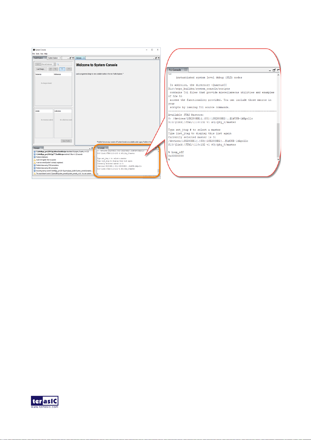
“test.bat” to program the FPGA and run the Tcl file (See Figure 6-4). The Tcl file will open the
Quartus tool “System Console” automatically(See Figure 6-5).
Figure 6-4 Execute demo batch file

Apollo Carrier Board
User Manual
51
www.terasic.com
May 8, 2020
Figure 6-5 Launch the System Console for Ethernet 40G Demo
6. If you have a QSFP28 loopback fixture installed, type “loop_off” to turns off internal serial
loopback. Otherwise, type “loop_on” to turn on internal serial loopback(See Figure 6-4).
Apollo Carrier Board
User Manual
52
www.terasic.com
May 8, 2020
Figure 6-6 Enter command for test
7. Type “start_pkt_gen” to starts the packet generator.
8. Type “chkmac_stats” to display the values in the MAC statics counters, as shown in Figure
6-7.

Apollo Carrier Board
User Manual
53
www.terasic.com
May 8, 2020
Figure 6-7 Ethernet 40G loopback test report for RX and TX

Apollo Carrier Board
User Manual
54
www.terasic.com
May 8, 2020
Date
Version
Changes
2020.04
First publication
2020.04
V1.1
Add chapter 5 &6
2020.05
V1.2
Add assemble and disassemble
board video in chapter 3
Chapter 7
Additional Information
7.1 Getting Help
Here are the addresses where you can get help if you encounter problems:
Terasic Technologies
9F., No.176, Sec.2, Gongdao 5th Rd,
East Dist, HsinChu City, Taiwan, 30070
Email: support@terasic.com
Web: www.terasic.com
Revision History
 Loading...