

Page 1
Page 2

CONTENTS
Chapter 1 Introduction of the HSMC-DVI ................................................................................................. 2
1.1 Features........................................................................................................................................................ 2
1.2 About the KIT .............................................................................................................................................. 3
1.3 Assemble the HSMC-DVI Board ................................................................................................................ 4
Chapter 2 HSMC-DVI Card Architecture .................................................................................................. 7
2.1 Layout and Components .............................................................................................................................. 7
2.2 Block Diagram of the DVI Board ................................................................................................................ 9
Chapter 3 Board Components ............................................................................................................. 10
3.1 HSMC Expansion Connector .................................................................................................................... 10
Chapter 4 Demonstrations ................................................................................................................... 17
4.1 Introduction ............................................................................................................................................... 17
4.2 System Requirements ................................................................................................................................ 18
4.3 Hardware Setup ......................................................................................................................................... 18
4.4 Configure FPGA ........................................................................................................................................ 18
4.5 Demo Operation ........................................................................................................................................ 19
4.6 Design Concept ......................................................................................................................................... 19
Chapter 5 Appendix ............................................................................................................................. 22
5.1 Revision History ........................................................................................................................................ 22
5.2 Always Visit HSMC-DVI Webpage for New Main board ......................................................................... 22
Page 3

Chapter 1
Introduction of the HSMC-DVI
The Terasic HSMC-DVI is a DVI transmitter/receiver board with a High Speed Mezzanine
Connector (HSMC) interface. It is designed to allow developers to access high quality and high
resolution video signals in their FPGA. It gives the flexibility required in high resolution image
processing systems by combining both the DVI transmitter and receiver onto the same card. Lastly,
the HSMC-DVI daughter board can be connected to any HSMC interface host boards.
11..1
1
FFeeaattuurreess
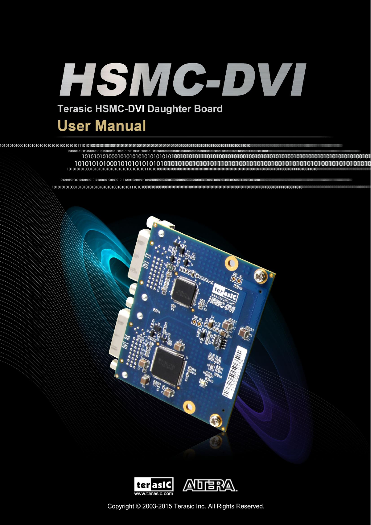
Figure 1-1 shows the photo of the HSMC-DVI board. The important features are listed below:
DDiiggiittaall TTrraannssmmiitttteerr
One DVI transmitter with single transmitting port
Digital Visual Interface (DVI) Compliant
Supports resolutions from VGA to UXGA (25 MHz – 165 MHz Pixel Rates)
Universal Graphics Controller Interface
。 12-Bit, Dual-Edge and 24-Bit, Single-Edge Input Modes
。 Standard 3.3 V CMOS Input Signal Levels
。 Fully Differential and Single-Ended Input Clocking Modes
。 Standard Intel 12-Bit Digital Video Port Compatible as on Intel™ 81x Chipsets
Enhanced PLL Noise Immunity
。 On-Chip Regulators and Bypass Capacitors for Reducing System Costs
Enhanced Jitter Performance
。 No HSYNC Jitter Anomaly
。 Negligible Data-Dependent Jitter
Programmable Using I²C Serial Interface
Single 3.3-V Supply Operation
DDiiggiittaall RReecceeiivveerr
Page 4
One DVI receiver with single receiving port
Supports UXGA Resolution (Output Pixel Rates Up to 165 MHz)
Digital Visual Interface (DVI) Specification Compliant
True-Color, 24 Bit/Pixel, 16.7M Colors at 1 or 2-Pixels Per Clock
Laser Trimmed Internal termination Resistors for Optimum Fixed Impedance Matching
4x Over-Sampling
Reduced Ground Bounce Using Time Staggered Pixel Outputs
Lowest Noise and Best Power Dissipation Using TI PowerPAD™ Packaging.
Figure 1-1 Layout of the DVI-HSMC card
11..2
2
AAbboouutt tthhee KKIITT
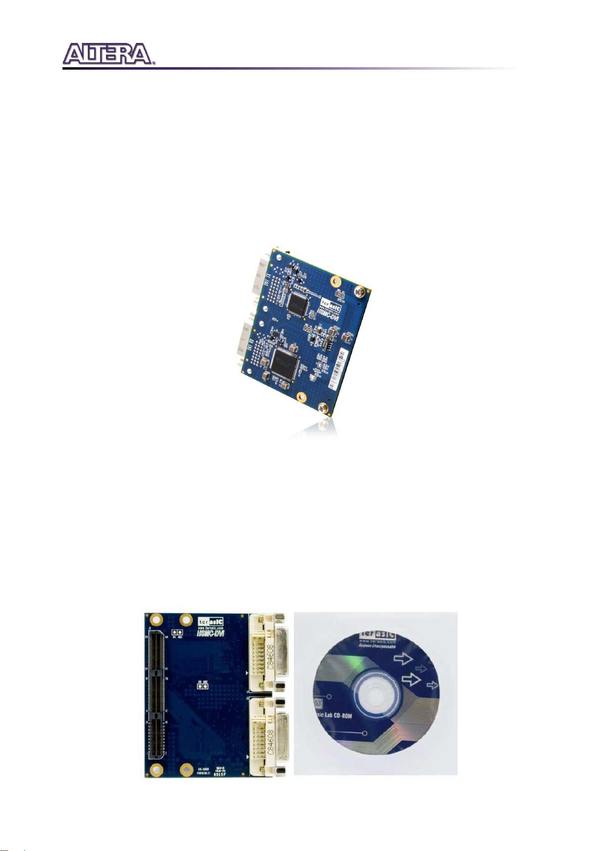
This section describes the package content:
HSMC-DVI board x 1
System CD-ROM x 1
Page 5
The CD contains technical documents of the HSMC-DVI, and one reference design along with the
source code. The source code of reference design are available for the following FPGA main board:
A5SK: Arria V Starter Kit
S5GFP: Stratix V GX FPGA Programmable Board
C5EFP: Cyclone V E FPGA Programmable Board
C5GFP: Cylone V GX FPGA Programmable Board
11..3
3
AAsssseemmbbllee tthhee HHSSMMCC--DDVVII BBooaarrdd
The Figure 1-1, Figure 1-1, Figure 1-1, and Figure 1-1 show how to connect the HSMC-DVI
daughter board to main boards.
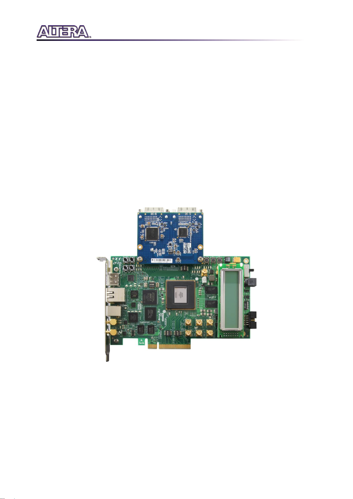
Figure 1-2 The HSMC-DVI board connects with A5SK
Page 6
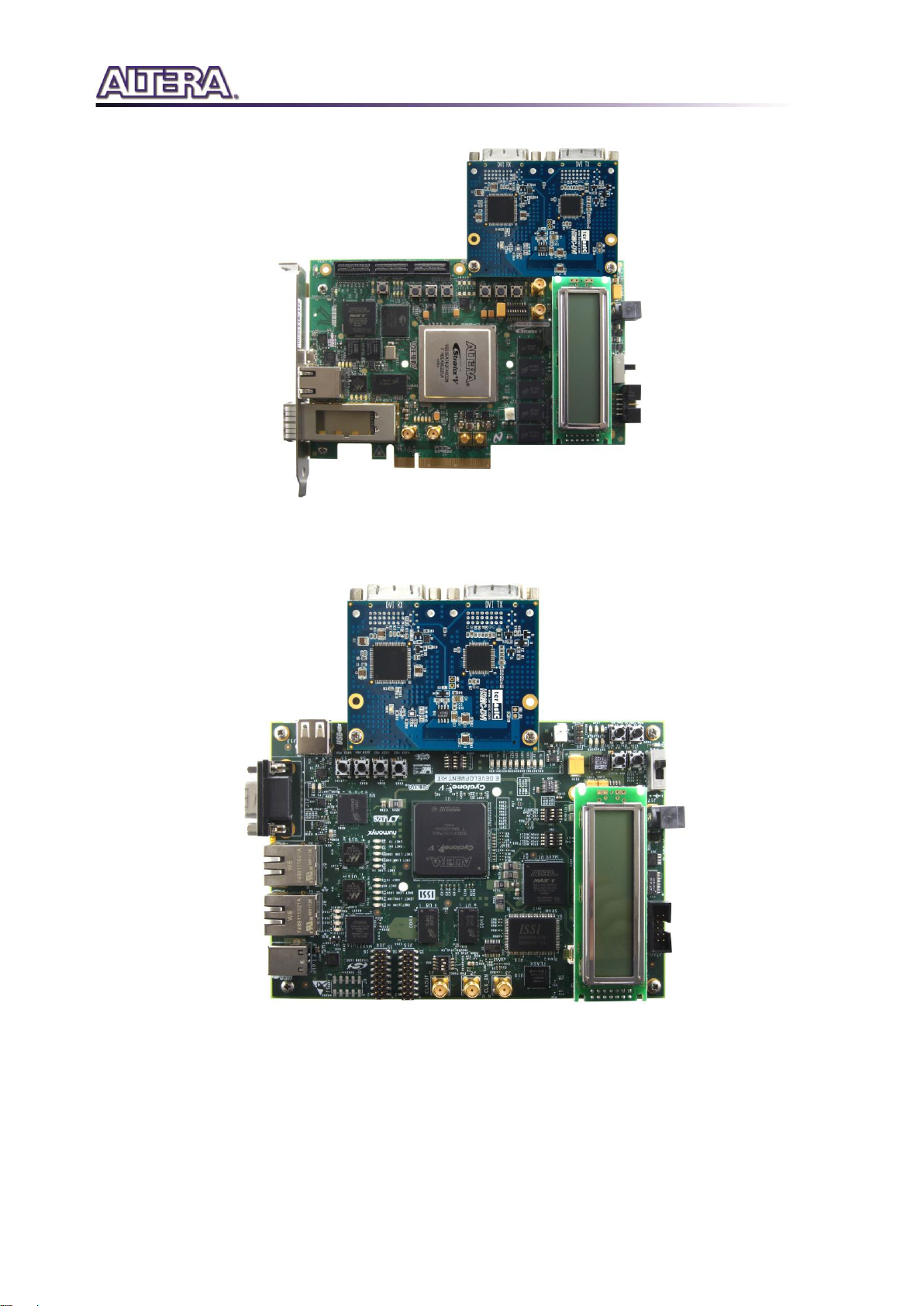
Figure 1-3 The HSMC-DVI board connects with S5GFP
Figure 1-4 The HSMC-DVI board connects with C5EFP
Page 7
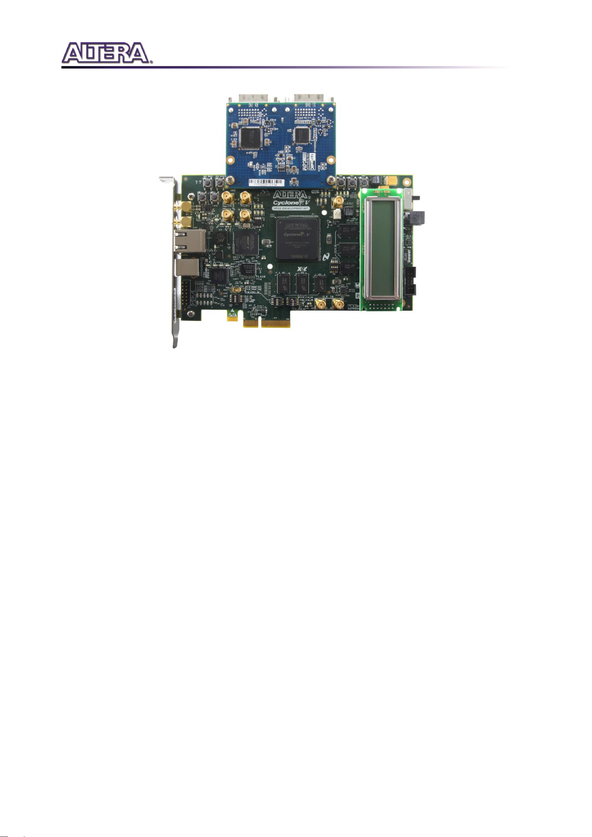
Figure 1-2 The HSMC-DVI board connects with C5GFP
Note. Do not attempt to connect/remove the HSMC-DVI daughter board to/from the main the
main board when the power is on, or else the hardware could be damaged.
11..44 GGeettttiinngg HHeellpp
Here are some places to get help if you encounter any problem:
• Email to support@terasic.com
• Taiwan & China: +886-3-575-0880
• Korea : +82-2-512-7661
• Japan: +81-428-77-700
Page 8

Chapter 2
HSMC-DVI Card Architecture
This Chapter covers the architecture of the HSMC-DVI board including its PCB and block diagram.
22..1
1
LLaayyoouutt aanndd CCoommppoonneennttss
The picture of the HSMC-DVI board is shown in Figure 2-1 and Figure 2-2 It depicts the layout of
the board and indicates the location of the connectors and key components.
Figure 2-1 The HSMC-DVI PCB and component diagram
Page 9

Figure 2-2 The HSMC-DVI Back side – HSMC connector vie
The following components are provided on the HSMC-DVI board :
• DVI Transmitter (U2)
• DVI Receiver (U3)
• I2C EEPROM (U4)
• DVI Transmitter Connector (J2)
• DVI Receiver Connector (J3)
• HSMC Connector (J1)
Page 10

22..2
2
BBlloocckk DDiiaaggrraamm ooff tthhee DDVVII BBooaarrdd
Figure 2-3 The block diagram of the HSMC-DVI board
Page 11

Chapter 3
Board Components
This section illustrates the detailed information of the components, connector interfaces, and the pin
mapping tables of the HSMC-DVI board.
33..1
1
HHSSMMCC EExxppaannssiioonn CCoonnnneeccttoorr
This section describes pin definition of the HSMC-DVI interface onboard. All the control and data
signals of the DVI transmitter and receiver are connected to the HSMC connector, so users can fully
control the HSMC-DVI daughter board through the HSMC interface. Power is derived from 3.3V
and 12V of the HSMC connector. Figure 2-1 shows the pin-outs on the HSMC connector.
Page 12

Figure 3-1 The pin-outs on the HSMC connecotor
Page 13

The Table 3-1 below lists the HSMC signal direction and description.
Note. The power pins are not shown in the table
Table 3-1
Pin Numbers
Name
Direction
Description
1
N.C.
N/A
Not Connect
2
N.C.
N/A
Not Connect
3
N.C.
N/A
Not Connect
4
N.C.
N/A
Not Connect
5
N.C.
N/A
Not Connect
6
N.C.
N/A
Not Connect
7
N.C.
N/A
Not Connect
8
N.C.
N/A
Not Connect
9
N.C.
N/A
Not Connect
10
N.C.
N/A
Not Connect
11
N.C.
N/A
Not Connect
12
N.C.
N/A
Not Connect
13
N.C.
N/A
Not Connect
14
N.C.
N/A
Not Connect
15
N.C.
N/A
Not Connect
16
N.C.
N/A
Not Connect
17
N.C.
N/A
Not Connect
18
N.C.
N/A
Not Connect
19
N.C.
N/A
Not Connect
20
N.C.
N/A
Not Connect
21
N.C.
N/A
Not Connect
22
N.C.
N/A
Not Connect
23
N.C.
N/A
Not Connect
24
N.C.
N/A
Not Connect
25
N.C.
N/A
Not Connect
26
N.C.
N/A
Not Connect
27
N.C.
N/A
Not Connect
28
N.C.
N/A
Not Connect
29
N.C.
N/A
Not Connect
30
N.C.
N/A
Not Connect
31
N.C.
N/A
Not Connect
32
N.C.
N/A
Not Connect
33
HSMC_SDA
Inout
I²C data
34
HSMC_SCL
Output
I²C clock
35
N.C.
N/A
Not Connect
36
N.C.
N/A
Not Connect
39
N.C.
N/A
Not Connect
Page 14

40
N.C.
N/A
Not Connect
41
DVI_RX_D0
Input
DVI receiver pixel data
42
DVI_RX_D14
Input
DVI receiver pixel data
43
DVI_RX_D1
Input
DVI receiver pixel data
44
DVI_RX_D15
Input
DVI receiver pixel data
45
3V3
Power
Power 3.3V
46
12V
Power
Power 12V
47
DVI_RX_D2
Input
DVI receiver pixel data
48
DVI_RX_D13
Input
DVI receiver pixel data
49
DVI_RX_D3
Input
DVI receiver pixel data
50
DVI_RX_D12
Input
DVI receiver pixel data
51
3V3
Power
Power 3.3V
52
12V
Power
Power 12V
53
DVI_RX_D4
Input
DVI receiver pixel data
54
DVI_RX_D11
Input
DVI receiver pixel data
55
DVI_RX_D5
Input
DVI receiver pixel data
56
DVI_RX_D10
Input
DVI receiver pixel data
57
3V3
Power
Power 3.3V
58
12V
Power
Power 12V
59
DVI_RX_D6
Input
DVI receiver pixel data
60
DVI_RX_D9
Input
DVI receiver pixel data
61
DVI_RX_D7
Input
DVI receiver pixel data
62
DVI_RX_D8
Input
DVI receiver pixel data
63
3V3
Power
Power 3.3V
64
12V
Power
Power 12V
65
DVI_RX_CTL1
Input
Control signal
66
DVI_RX_D7
Input
DVI receiver pixel data
67
DVI_RX_HS
Input
DVI receiver horizontal sync
68
DVI_RX_D6
Input
DVI receiver pixel data
69
3V3
Power
Power 3.3V
70
12V
Power
Power 12V
71
DVI_RX_VS
Input
DVI receiver vertical sync
72
DVI_RX_D5
Input
DVI receiver pixel data
73
DVI_RX_DE
Input
DVI receiver pixel data
74
DVI_RX_D4
Input
DVI receiver pixel data
75
3V3
Power
Power 3.3V
76
12V
Power
Power 12V
77
DVI_RX_CTL3
Input
Control signal
78
DVI_RX_D3
Input
DVI receiver pixel data
79
DVI_RX_CTL2
Input
Control signal
80
DVI_RX_D2
Input
DVI receiver pixel data
81
3V3
Power
Power 3.3V
82
12V
Power
Power 12V
Page 15

83
DVI_RX_DDCS
DA
Inout
DDC I²C data
84
DVI_RX_D1
Input
DVI receiver pixel data
85
DVI_RX_DDSC
L
Inout
DDC I²C clock
86
DVI_RX_D0
Input
DVI receiver pixel data
87
3V3
Power
Power 3.3V
88
12V
Power
Power 12V
89
EDID_WP_n
Output
I²C write protect enable
90
DVI_RX_SCDT
Input
Receiver sync detect
91
N.C.
N/A
Not Connect
92
DVI_TX_D17
Output
DVI transmitter data bus
93
3V3
Power
Power 3.3V
94
12V
Power
Power 12V
95
DVI_TX_D16
Output
DVI transmitter data bus
96
DVI_RX_CLK
Input
DVI receiver clock
97
N.C.
N/A
Not Connect
98
N.C.
N/A
Not Connect
99
3V3
Power
Power 3.3V
100
12V
Power
Power 12V
101
DVI_TX_D12
Output
DVI transmitter data bus
102
DVI_TX_D18
Output
DVI transmitter data bus
103
DVI_TX_D13
Output
DVI transmitter data bus
104
DVI_TX_D19
Output
DVI transmitter data bus
105
3V3
Power
Power 3.3V
106
12V
Power
Power 12V
107
DVI_TX_D14
Output
DVI transmitter data bus
108
DVI_TX_D20
Output
DVI transmitter data bus
109
DVI_TX_D15
Output
DVI transmitter data bus
110
DVI_TX_D21
Output
DVI transmitter data bus
111
3V3
Power
Power 3.3V
112
12V
Power
Power 12V
113
DVI_TX_D11
Output
DVI transmitter data bus
114
DVI_TX_D22
Output
DVI transmitter data bus
115
DVI_TX_D10
Output
DVI transmitter data bus
116
DVI_TX_D23
Output
DVI transmitter data bus
117
3V3
Power
Power 3.3V
118
12V
Power
Power 12V
119
DVI_TX_D9
Output
DVI transmitter data bus
120
DVI_TX_DKEN
Output
Data de-skew enable
121
DVI_TX_D8
Output
DVI transmitter data bus
122
DVI_TX_HS
Output
DVI transmitter Horizontal
sync
Page 16

123
3V3
Power
Power 3.3V
124
12V
Power
Power 12V
125
DVI_TX_D7
Output
DVI transmitter data bus
126
DVI_TX_VS
Output
DVI transmitter vertical sync
127
DVI_TX_D6
Output
DVI transmitter data bus
128
DVI_TX_CTL3
Output
Multifunction
129
3V3
Power
Power 3.3V
130
12V
Power
Power 12V
131
DVI_TX_D5
Output
DVI transmitter data bus
132
DVI_TX_CTL2
Output
Multifunction
133
DVI_TX_D4
Output
DVI transmitter data bus
134
DVI_TX_CTL1
Output
Multifunction
135
3V3
Power
Power 3.3V
136
12V
Power
Power 12V
137
DVI_TX_D3
Output
DVI transmitter data bus
138
DVI_TX_HTPL
G
Output
Edge select/hot plug input
139
DVI_TX_D2
Output
DVI transmitter data bus
140
TX_PD_n
Output
Power down (active low)
141
3V3
Power
Power 3.3V
142
12V
Power
Power 12V
143
DVI_TX_D1
Output
DVI transmitter data bus
144
DVI_TX_MSEN
Input
Monitor sense/programmable
output
145
DVI_TX_D0
Output
DVI transmitter data bus
146
DVI_TX_ISEL
Output
I²C interface select/I²C reset
147
3V3
Power
Power 3.3V
148
12V
Power
Power 12V
149
DVI_TX_DE
Output
DVI data enable
150
DVI_TX_SDA
I/O
DSEL/I²C data
151
DVI_TX_DDCS
DA
I/O
DDC I²C data
152
DVI_TX_SCL
Output
Input bus select/I²C clock
153
3V3
Power
Power 3.3V
154
12V
Power
Power 12V
155
DVI_TX_CLK
Output
DVI transmitter clock
156
N.C.
N/A
Not Connect
157
DVI_TX_DDCS
CL
Output
DDC I²C clock
158
N.C.
N/A
Not Connect
159
3V3
Power
Power 3.3V
160
GND
Power
Power Ground
161
GND
Power
Power Ground
Page 17

162
GND
Power
Power Ground
163
GND
Power
Power Ground
164
GND
Power
Power Ground
165
GND
Power
Power Ground
166
GND
Power
Power Ground
167
GND
Power
Power Ground
168
GND
Power
Power Ground
169
GND
Power
Power Ground
170
GND
Power
Power Ground
171
GND
Power
Power Ground
172
GND
Power
Power Ground
Page 18

Chapter 4
Demonstrations
This Chapter illustrates the reference design for the HSMC-DVI board.
44..1
1
IInnttrroodduuccttiioonn
This section describes the functionality of the demonstration briefly.
The demonstration shows how to use Altera’s 28nm-FPGA development kits to interface with the
HSMC-DVI board, which include:
• Stratix V GX FPGA Development Kit features a 5SGXEA7K2F40C2 device
• Arria V GX Starter Kit features a 5AGXFB3H4F35C5 device
• Cyclone V GX FPGA Development Kit features a 5CGXFC7D7F31C8ES device
• Cyclone V E Development Kit features a 5CEFA7F31C7ES device
The demonstration includes two parts:
Transmission Demo:
The reference design can generate various video format signals for transmission. The supported
formats include:
Pattern ID
Video Format
PCLK (MHZ)
0
640x480@60P
25 1 720x480@60P
27 2 1024x768@60P
65 3 1280x1024@60P
108 4 1920x1080@60P
148.5
5
1600x1200@60P
162
Loopback Demo:
Page 19

Loopback the DVI video signals within the FPGA board (internal bypass). The video output pins of the
receiver are directly connected to the input video pins of the transmitter.
44..2
2
SSyysstteemm RReeqquuiirreemmeennttss
The following items are required for the HSMC-DVI Server demonstration.
• HSMC-DVI Daughter Card x 1
• Altera’s FPGA development kit x 1
• LCD monitor with at least one DVI input x 1
• DVI Video source x 1
• DVI Cable x 2
44..3
3
HHaarrddwwaarree SSeettuupp
Figure 4-1 shows how to setup hardware for the HSMC-DVI demonstration.
Figure 4-1 Demonstration Hardware setup
44..4
4
CCoonnffiigguurree FFPPGGAA
This section describes the procedures of configure the FPGA. Please follow the procedure below to
configure FPGA:
1. Connect the Altera FPGA development board to your PC via USB cable.
2. Power on the Altera FPGA development board
Page 20

3. Configure the FPGA by programming the bit stream file: DVI_Demo.sof
The bit stream file is located in the project directory as shown below:
• Stratix V GX FPGA Development Kit: S5GFP_DVI
• Arria V GX Starter Kit: A5SK_DVI
• Cyclone V GX FPGA Development Kit: C5GFP_DVI
• Cyclone V E Development Kit: C5EFP_DVI
44..5
5
DDeemmoo OOppeerraattiioonn
This section describes the procedures of operation the demonstration.
DVI Transmission Demo:
For the transmission demonstration, please connect a DVI-compatible monitor to the DVI-TX port
of the HSMC-DVI daughter card with a DVI cable.
By pressing PB[0] you can toggle between the transmission Demo and Loopback Demo. Pressing
PB[1] can change active transmission pattern. When transmission demo is active, LED[7:3] are off.
The associated pattern ID is indicated by LED[2:0].If LED[2:0] are all off, the pattern ID is zero.
DVI Loopback Demo:
For the loopback demonstration, please connect a DVI-compatible monitor to the DVI-TX port of
the HSMC-DVI daughter card and attach a DVI video source to the respective DVI-RX port with
DVI cables.
By pressing PB[0] you can toggle between the transmission Demo and Loopback Demo. When
loopback demo is active, LED[7:0] are on.
44..6
6
DDeessiiggnn CCoonncceepptt
This section describes the design concepts for the HSMC-DVI demonstration. Figure 4-2 show the
block diagram of the demonstration.
Page 21

Figure 4-2 Block diagram
The “Video Pattern Generator” module corresponds to the generated test patterns for transmission
demo. The test patterns include:
Pattern ID
Video Format
PCLK (MHZ)
Page 22

0
640x480@60P
25
1
720x480@60P
27
2
1024x768@60P
65
3
1280x1024@60P
108
4
1920x1080@60P
148.5
5
1600x1200@60P
162
The display resolution and pixel rate will change when the mode changes. In this module, the Altera
IP “PLL Reconfig” is used to set various pixel rates to the Altera IP “PLL”. The RECONFIG data
for various clocks are from “PLL Controller”. The module source code is located in the
“vpg_source” sub-folder. For more information about Altera’s re-configuration PLL IP , please
refer to http://www.altera.com/literature/lit-an.jsp
The “Video Source Selector” module corresponds to the selected desired video source for final
video display.
Page 23

Chapter 5
Appendix
55..1
1
RReevviissiioonn HHiissttoorryy
Version
Change Log
June 25 , 2009
Initial Version (Preliminary)
July 28 , 2015
Modify function block
Nov 22, 2017
Modify the Universal Graphics Controller Interface description
55..2
2
AAllwwaayyss VViissiitt HHSSMMCC--DDVVII WWeebbppaaggee ffoorr NNeeww MMaaiinn bbooaarrdd
Copyright © 2015 Terasic Technologies. All rights reserved.
We will be continuing providing interesting examples and labs on our HSMC-DVI
webpage. Please visit www.altera.com or dvi.terasic.com for more information.
 Loading...