

Page 1
Altera DE3 Board
Page 2

Altera DE3 Board
ii
CONTENTS
Chapter 1 Overview ........................................................................................................................... 1
1.1 Introduction .......................................................................................................................... 1
1.2 Layout and Components ...................................................................................................... 1
1.3 Block Diagram of the DE3 Board ........................................................................................ 4
Chapter 2 Using the DE3 Board ....................................................................................................... 8
2.1 Configuring the FPGA and Serial Configuration Device .................................................... 8
2.2 JTAG Chain ........................................................................................................................ 10
2.3 Using the User I/O Interface .............................................................................................. 13
2.4 I/O Groups and V
CCIO
Control Circuit ............................................................................... 14
2.5 Using the HSTC Connectors .............................................................................................. 17
2.6 Connecting HSTC/HSMC Daughter Boards to DE3 HSTC connectors ........................... 20
2.7 Using the GPIO Expansion Headers .................................................................................. 20
2.8 Using the DDR2 SO-DIMM .............................................................................................. 21
2.9 Using the USB OTG .......................................................................................................... 22
2.10 Using the SD Card ............................................................................................................. 23
2.11 LED Indicators ................................................................................................................... 24
2.12 Clock Circuitry ................................................................................................................... 24
2.13 Using the Temperature Sensor ........................................................................................... 27
Chapter 3 Control Panel .................................................................................................................. 28
3.1 Control Panel Setup ........................................................................................................... 28
3.2 Controlling the LEDs and 7-Segment Displays ................................................................. 31
3.3 SWITCH/BUTTON ........................................................................................................... 33
3.4 Memory Controller ............................................................................................................ 33
3.5 USB2.0 OTG ...................................................................................................................... 35
3.6 SD CARD .......................................................................................................................... 36
3.7 Temperature Monitor ......................................................................................................... 37
3.8 I/O Group ........................................................................................................................... 38
3.9 Overall Structure of the DE3 Control Panel ...................................................................... 40
Chapter 4 DE3 System Builder ....................................................................................................... 41
4.1 Introduction ........................................................................................................................ 41
4.2 General Design Flow ......................................................................................................... 41
4.3 Using DE3 System Builder ................................................................................................ 43
4.4 Creating My First DE3 Project .......................................................................................... 49
4.5 Connect TERASIC Daughter Boards to a DE3 Board ...................................................... 50
4.6 Connect Multiple DE3 Boards ........................................................................................... 53
4.7 Connect a Custom-Made Daughter Board to the DE3 Board ............................................ 56
Page 3

Altera DE3 Board
iii
Chapter 5 Examples of Advanced Demonstration ........................................................................ 58
5.1 USB Host ........................................................................................................................... 58
5.2 USB Device........................................................................................................................ 65
5.3 SD Card .............................................................................................................................. 68
5.4 DDR2 SDRAM .................................................................................................................. 73
Appendix A Pin connections between components and FPGA on the DE3 board ..................... 80
Appendix B Pin Compatible List for HSTC and HSMC Connector .......................................... 98
Appendix C Programming the Serial Configuration Device ..................................................... 102
Appendix D DE3_HSTC Utility .................................................................................................... 108
Appendix E LVDS Termination Resistors ................................................................................... 112
Additional Information.................................................................................................................. 114
Getting Help ................................................................................................................................. 114
Revision History .......................................................................................................................... 114
Page 4
DE3 User Manual
1
Chapter 1
Overview
1
This chapter presents the features and design characteristics of the DE3 board.
1.1 Introduction
The DE3 board has plenty of features that allow users to implement a wide range of designed
circuits. The Stratix® III device is capable of dealing with resource-consuming projects and
complex algorithm verification; the HSTC interface is equipped for high-speed inter-connection and
configurable I/O standards. The DDR2 SO-DIMM socket puts the experience of faster memory
access into practice, while the SD card socket provides the realization of data storage extension.
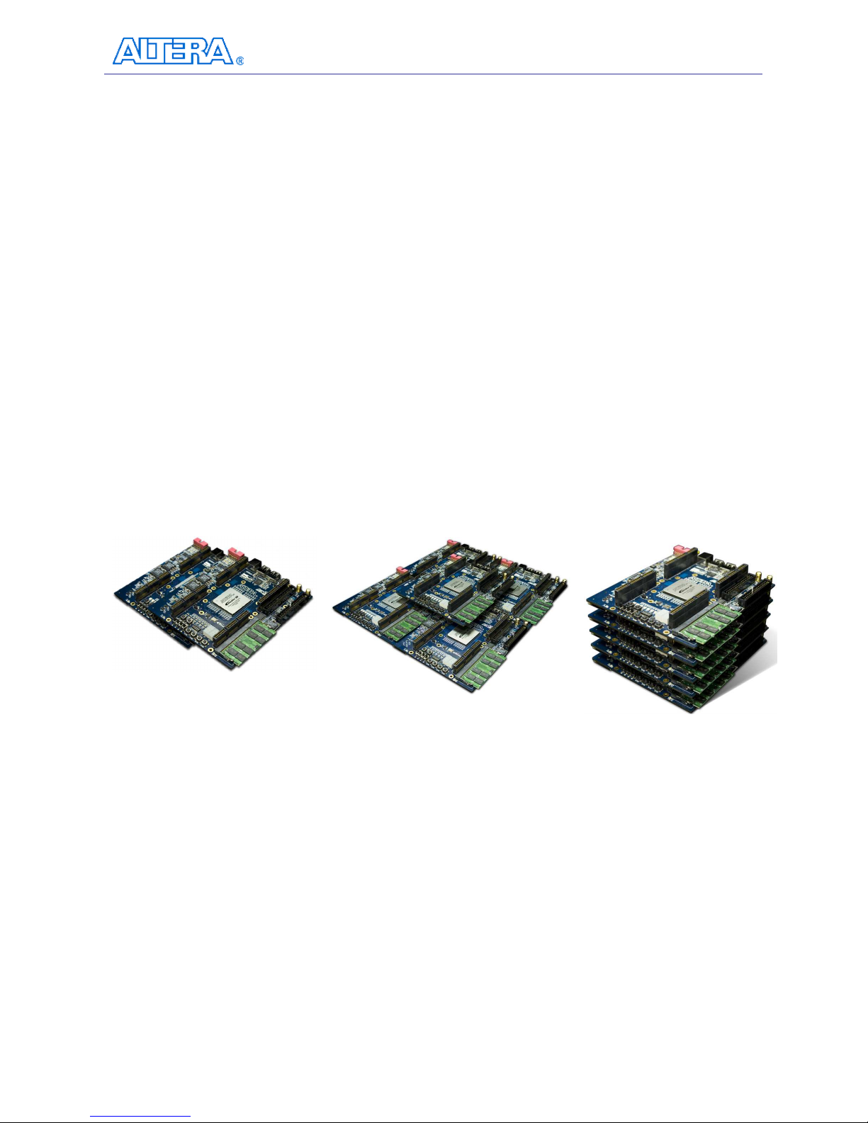
In addition, the DE3 board has an innovative stackable mechanism which allows users to assemble
DE3 boards into a powerful system as shown in Figure 1.1. The DE3 can also connect with multiple
daughter boards designed by Terasic in stock.
Figure 1.1 The stackable mechanism of the DE3 board
1.2 Layout and Components
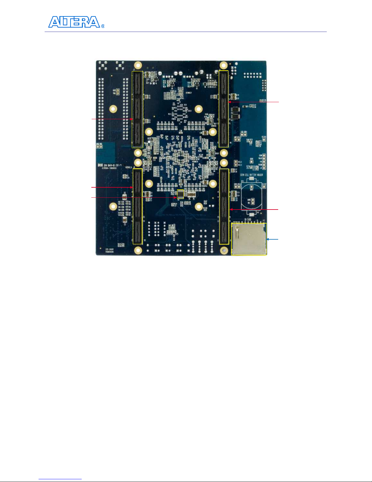
Figure 1.2 and Figure 1.3 is the top and bottom view of the DE3 board. It depicts the layout of the
board and indicates the location of the connectors and key components. Users can refer to this
figure for relative location when the connectors and key components are introduced in the following
chapters.
Page 5
DE3 User Manual
2
50MHz Oscillator
Expansion Header 2
SMA External Clock In
DDR2 SO-DIMM Socket
4 Slide Switches
7-Segment Displays
Altera USB Blaster
Controller Chipset
Altera EPCS128 / EPCS64
Configuration Device
USB Host/Device
Controller
HSTC Bottom Side
Enable
8 RGB LEDs
Expansion Header 1
4 Push-Button Switches
USB Blaster
Power ON/OFF Switch
Power Supply
Connector
USB Device
SD Card Slot
USB Device
USB Host/Device SMA PLL Clock Out
Altera Stratix III
3SL340 (DE3-340)
or
3SL260 (DE3-260)
or
3SL150 (DE3-150)
Reconfigure Switch
CPU RESET Switch
8-Position Dip Switch
HSTC Connector C
HSTC Connector D
HSTC Connector B
HSTC Connector A
+12V Fan Connector
Figure 1.2 The DE3 board (Top view)
Page 6
DE3 User Manual
3
Temperature Sensor
HSTC connector B
HSTC connector A
HSTC connector C
SD Card Slot
HSTC connector D
Figure 1.3. The DE3 board (Bottom view)
The following hardware is implemented on the DE3 board:
• Altera Stratix® III FPGA device (3SL340/3SE260/3SL150)
• FPGA configuration interface:
Built-in USB Blaster circuit for programming and user API control
Altera Serial Configuration device – EPCS128/EPCS64
• Expansion Interface:
8 HSTC connectors
Two 40-pin Expansion Headers
• Memory Interface:
DDR2 SO-DIMM socket
SD Card socket
Page 7

DE3 User Manual
4
• User I/O Interface:
4 push-button switches
4 slide switches
1 eight position DIP switch
2 seven-segment displays
8 RGB LEDs
• Clock system
One 50MHz oscillator
2 SMA connectors for external clock input and PLL clock output
• Other interface
1 USB Host/Slave controller(1 three-ports USB Host/Device controller)
1 temperature sensor chip for FPGA temperature measurement
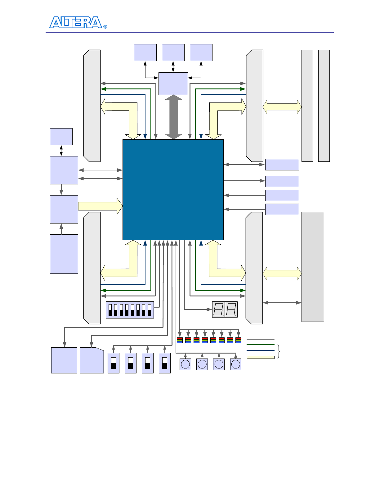
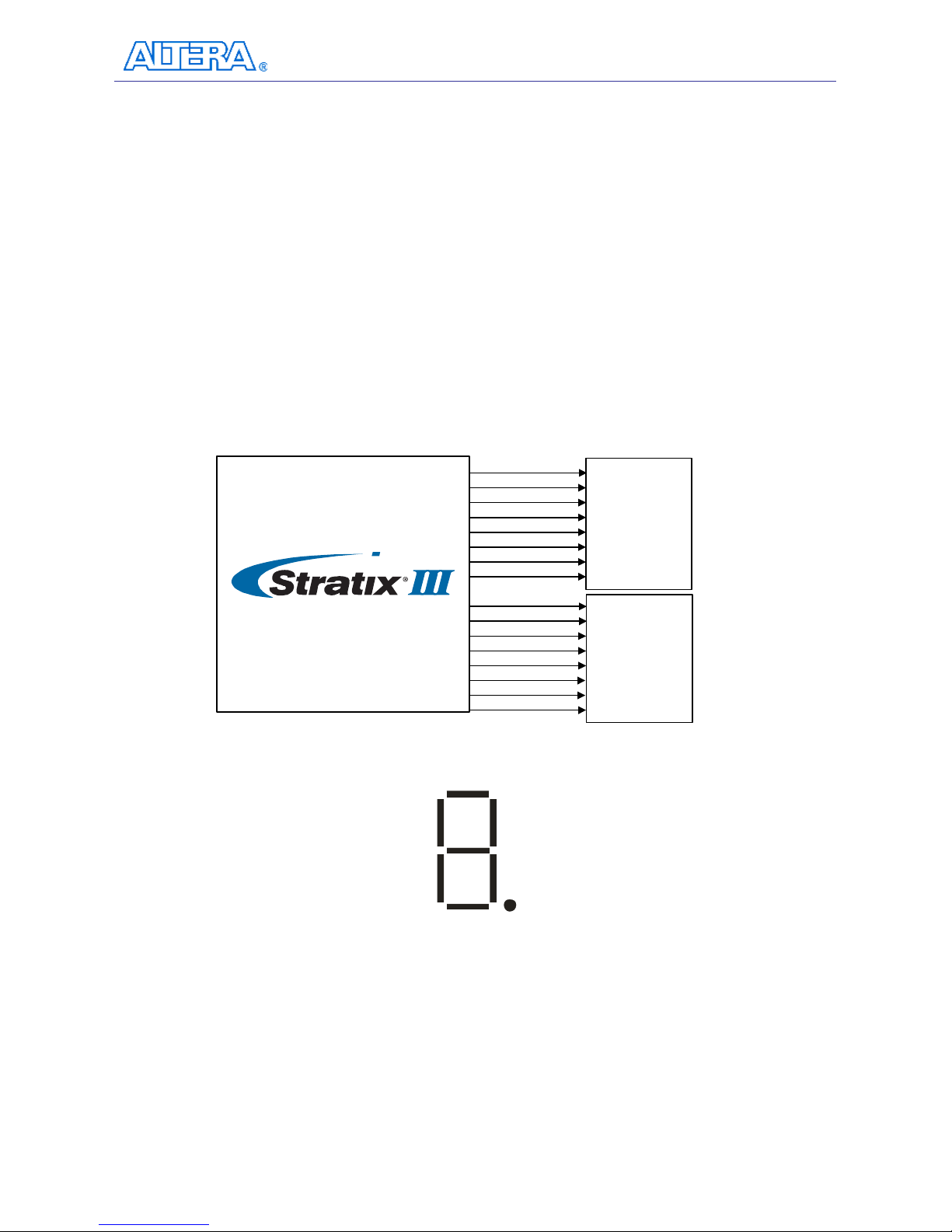
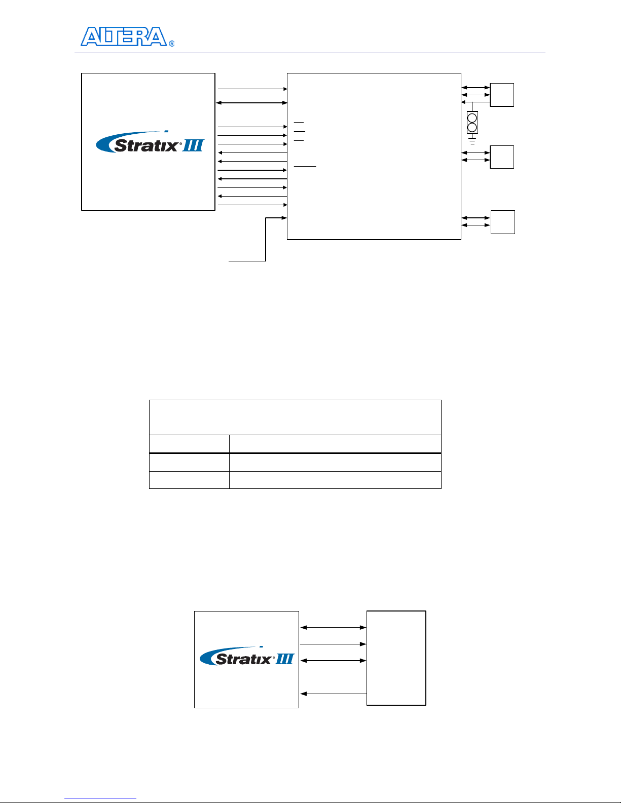
1.3 Block Diagram of the DE3 Board
Figure 1.4 shows the block diagram of the DE3 board. To provide maximum flexibility for the users,
all key components are connected with the Stratix III FPGA device. Thus, users can configure the
FPGA to implement any system design.
Page 8
DE3 User Manual
5
Power
1.1V
3.3V
5.0V
12V
GPIO 0
EPCS128
HOST
CON
x120
USB
Hi-Speed
OTG
x60
HSTC C
HSTC B
HSTC A
HSTC D
DDR2 SO-DIMM
x120 x120
x120
Clock IN x5
Clock OUT x5
Clock IN x5
Clock OUT x5
Clock IN x5
Clock OUT x5
1.5V
1.8V
2.5V
3.3V
VCCIO(BA,BB,BC,BD)
PLL_OUT
CLOCK_IN
Clock IN x5
Clock OUT x5
HOST
CON
DEVICE
CON
GPIO 1
x80
PLL OUT
CLOCK IN
50 MHz
OSC
OSC x6
EPM240
JTAG x4
USB
CON
7-Seg x 16
DIP Switch x 8
I2C x2
I2C x2
I2C x2
I2C x2
JVC x4
Select and
Power ON
I2C x2
Stratix III
EP3SL150F1152/
EP3SL340F1152/
EP3SE260F1152
Adjustable Voltage Signal
3.3V
Bank I/O Voltage
3.3V Signal
SD Card
Socket
Button Switch x4
Color LED x 24
Slider Switch x4
SD Card x 4
x120
Temperature
Sensor
Temp. Sensor x 6
Figure 1.4 Block diagram of the DE3 board
Page 9

DE3 User Manual
6
Below is more detailed information regarding the blocks in
Figure 1.4:
Stratix III FPGA
•
EP3SL340
- 338,000 logic elements (LEs)
- 18,381K Total Memory Kbits
- 526 18x18-bit Multipliers blocks
- 12 phase-locked-loops (PLLs)
-
•
EP3SE260
- 254,400 logic elements (LEs)
- 16,282K Total Memory Kbits
- 768 18x18-bit Multipliers blocks
- 12 phase-locked-loops (PLLs)
•
EP3SL150
- 142,000 logic elements (LEs)
- 6,390K Total Memory Kbits
- 384 18x18-bit Multipliers blocks
- 8 phase-locked-loops (PLLs)
Serial Configuration device and USB Blaster circuit
• Altera’s EPCS128/EPCS64 Serial Configuration device
• On-board USB Blaster for programming and user API control
• Support JTAG mode
DDR2 SO-DIMM socket
• Up to 4GB capacity
• Share the same I/O bus with HSTC connector B
SD card socket
• Provides SPI and 1-bit SD mode for SD Card access
Page 10

DE3 User Manual
7
Push-button switches
• 6 push-button switches
- 1 CPU Reset
- 1 FPGA Reconfigure
- 4 user-defined inputs
• Debounced by a Schmitt trigger circuit
• Normally high; generates one active-low pulse when the switch is pressed
Slide switches
• 4 slide switches for user-defined inputs
• When a switch is set to the DOWN or UP position (i.e., close to or away from the edge of
the DE3 board), it causes logic 0 or 1, respectively.
Clock inputs
• 50MHz oscillator
• 1 SMA connector for PLL clock output
• 1 SMA connector for external clock input
USB Host/Slave controller
• Complies fully with Universal Serial Bus Specification Rev. 2.0
• Support data transfer at high-speed, full-speed, and low-speed
• Support both USB host and device
• Three USB ports (one type mini-AB for host/device and two type A for host)
• Support Nios II with the Terasic driver
• Support Programmed I/O (PIO) and Direct Memory Access (DMA)
Eight 180-pin High Speed Terasic Connectors (HSTC) expansion headers
• 4 male and 4 female connectors are on the top and the bottom of DE3 board, respectively.
• 240 LVDS pairs of user-defined IO pins
• Configurable I/O voltage for 3.3V, 2.5V, 1.8V, and 1.5V
Two 40-pin expansion headers
• 72 FPGA I/O pins, as well as 8 power and ground lines, are brought out to two 40-pin
expansion connectors
• 40-pin header is designed to accept a standard 40-pin ribbon cable used for IDE hard drives
• Share the same I/O pins with HSTC connector A
Page 11

DE3 User Manual
8
Chapter 2
Using the DE3 Board
2
This chapter gives instructions for using the DE3 board and its components.
It is strongly recommended that users should read the Getting Started with the Altera DE3 board.pdf
before using the DE3 board. The document is located in the DE3_usermanual folder on the DE3
System CD. The contents of the document includes following:
1. Purpose of the DE3 Board
2. Scope of the DE3 Board and Supporting Material
3. Installing the Altera Design Software
4. Obtain a License File from Altera’s website
5. Setup the License File for Terasic Power Controller IP.
6. Install the USB Blaster Driver
7. Power up the DE3 Board
8. Programming the FPGA Device on the DE3 Board
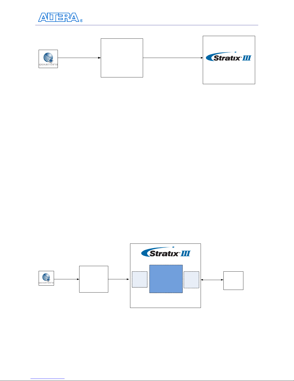
2.1 Configuring the FPGA and Serial Configuration Device
Programming the FPGA device:
The DE3 board has a built-in USB Blaster circuit, which allows users to program the FPGA
device using USB cable and Quartus II programmer in JTAG mode. Current configuration will
be lost when the power is turned off.
To download a configuration bit stream into the Stratix III FPGA, perform the following steps:
• Make sure that power is provided to the DE3 board
• Connect the USB cable supplied to the USB Blaster port of the DE3 board (see Figure 2.1)
• The FPGA can now be programmed in the Quartus II Programmer by selecting a
configuration bit stream file with the .sof filename extension.
Please refer to Getting Started with the Altera DE3 board.pdf for more detailed procedure of
FPGA programming.
Page 12
DE3 User Manual
9
Quartus II
Programmer
USB Blaster
Circuit
JTAG Config Signals
JTAGUART
Figure 2.1 The JTAG configuration scheme
Programming the serial configuration device :
The DE3 board contains a serial configuration device (U4) that stores configuration data for
the Stratix III FPGA. This configuration data is automatically loaded from the serial
configuration device chip into the FPGA when the board is powered up.
Since the Active Serial programming interface is not supported on the DE3 board, users will
need to use a Serial Flash Loader (SFL) function to program the serial configuration device via
the JTAG interface. The FPGA-based SFL is a soft intellectual property (IP) core within the
FPGA that bridges the JTAG and flash interfaces. The SFL mega-function is available from
Quartus II software. Figure 2.2 shows the programming method when adopting a SFL solution.
Please refer to Appendix C Programming the Serial Configuration device for the basic
programming instruction on the serial configuration device. More detailed information on the
SFL mega-function can be found in Altera Application Note 370: Using the Serial Flash
Loader With the Quartus II Software.
Quartus II
Programmer
USB Blaster
Circuit
Serial Configuration Device
JTAG
EPCS
128
SFL Image
to bridge
The
JTAG and ASMI
JTAG
ASMI
Figure 2.2. Programming a serial configuration device with the SFL solution
Page 13
DE3 User Manual
10
2.2 JTAG Chain
This section describes how to setup the JTAG chain on DE3 board.
If the DE3 board is used without any board connected and all the positions in SW6 are switched to
OFF (i.e., down position), the JTAG-interface signals of all HSTC connectors are bypassed, as
shown in Figure 2.3.
When the top HSTC connector is not connected with any daughter board, the JTGA interface is
bypassed. If a daughter board is connected to the top HSTC connector, the JTAG interface will be
enabled automatically. Figure 2.4 shows the JTAG chain with a daughter board connected to the
DE3 board via top HSTC connector A. Note that if the daughter board does not use the JTAG
interface, the TDI and TOD pins on the daughter board must be shorted for the JTAG signals to pass
through.
A four position DIP switch (SW6) on DE3 board is used to control the JTAG interface signals of
bottom HSTC connectors. Table 2-1 indicates the detailed configurations of SW6. When the bottom
connector is connected with other DE3 board or an daughter board, users need to configure the
SW6 to connect the JTAG chain to other board accordingly. Figure 2.5 shows there are two DE3
boards stacked, and the JTAG chain is established through HSTA connector A, as shown in Figure
2.6.
Table 2-1. DIP switch (SW6) setting for JTAG interface on bottom HSTC connectors
Position
Switch Setting
Turn OFF (lower position) Turn ON (upper position)
1
Bypass the JTAG interface on
the Bottom HSTC connector A(J2)
Enable the JTAG interface for
Bottom HSTC connector A(J2)
2
Bypass the JTAG interface on
the Bottom HSTC connector B(J4)
Enable the JTAG interface for
Bottom HSTC connector B(J4)
3
Bypass the JTAG interface on
the Bottom HSTC connector C(J6)
Enable the JTAG interface for
Bottom HSTC connector C(J6)
4
Bypass the JTAG interface on
the Bottom HSTC connector D(J8)
Enable the JTAG interface for
Bottom HSTC connector D(J8)
Page 14
DE3 User Manual
11
TDI TDO
TDO
TDI
USB Blaster
Circuit
USB
Cable
Host
PC
Statix III FPGA
DE3 Board
OFF
OFF
OFF
OFF
SW6
HSTC Connector A
Bypassed
HSTC Connector B
Bypassed
HSTC Connector C
Bypassed
HSTC Connector D
Bypassed
2
3
4
1
Figure 2.3. JTAG chain for a standalone DE3 board
TDOTDI
TDI TDO
HSTC Connector
A Top
TDI TDO
TDO
TDI
USB
Blaster
Circuit
USB
Cable
Host
PC
Stratix III FPGA
Daughter
Board
DE3 Board
OFF
OFF
OFF
OFF
SW6
Figure 2.4. JTAG chain for a daughter board connected with DE3 board via top HSTC connector A
Page 15

DE3 User Manual
12
Figure 2.5. The two DE3 boards stacked and the JTAG path is established through HSTC connector
A.
TDO TDI
HSTC Connector A
Bottom
TDI TDO
TDO
TDI
USB
Blaster
Circuit
USB
Cable
Host
PC
TDOTDI
HSTC Connector A
Top
TDI TDO
TDO
TDI
USB
Blaster
Circuit
SW6
1
2
3
4
ON
OFF
DE3 Board 1
DE3 Board 2
OFF
OFF
Stratix III FPGA
Stratix III FPGA
SW6
1
2
3
4
OFF
OFF
OFF
OFF
Figure 2.6. JTAG chain for two stacked DE3 boards
Page 16
DE3 User Manual
13
2.3 Using the User I/O Interface
Push-Button Switches:
The DE3 board provides four user-defined, one CPU reset, and one Reconfigure push-button
switches. The Reconfigure push-button is used to force a re-boot of the FPGA from the serial
configuration device.
The CPU reset push-button is an input to the Stratix III device. It is intended to be the master
reset signal for the FPGA designs loaded into the Stratix III device. The CPU reset push
-button is connected to the DEV_CLRn pin on the FPGA. The DEV_CLRn setting is a pin
option in the Quartus II software that users must enable to function the CPU reset as
DEV_CLRn instead of a standard I/O.
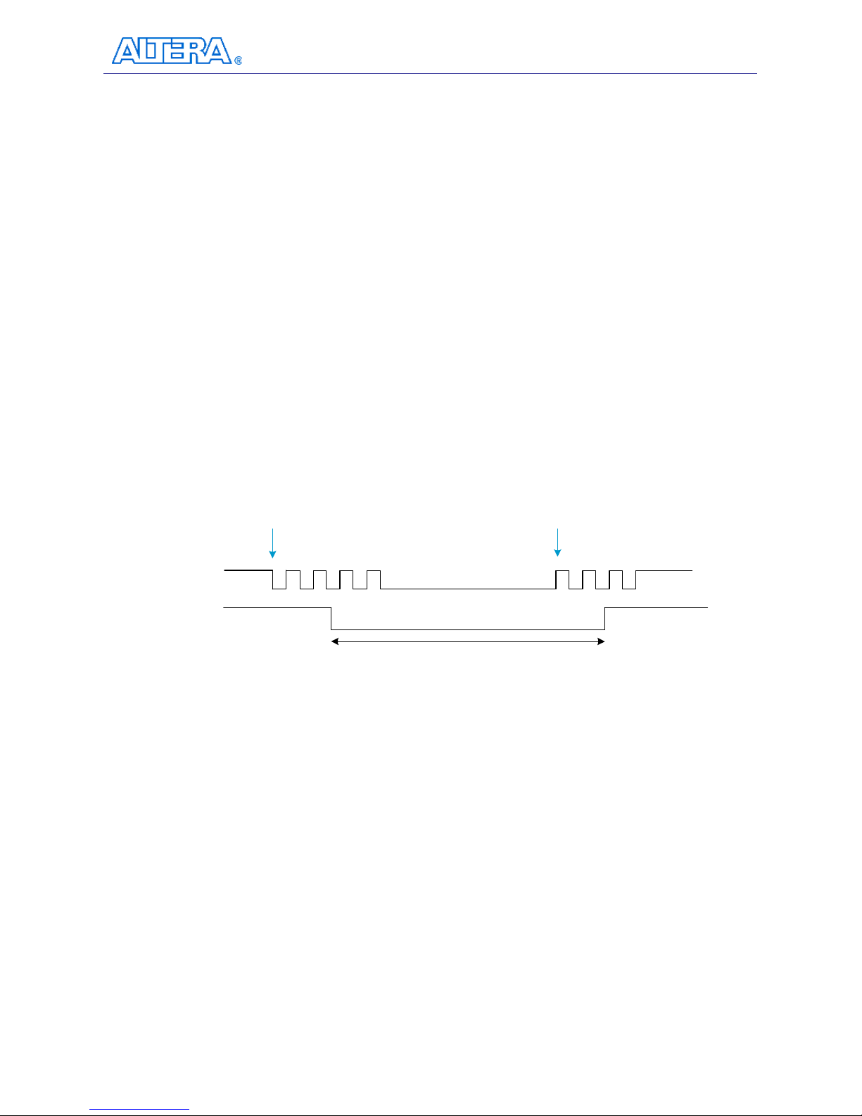
Each of these switches is de-bounced using a Schmitt Trigger circuit, as indicated in Figure
2.7. Each push-button provides a high logic level (3.3 volts) or a low logic level (0 volts)
when it is not pressed or pressed, respectively. Table A-1 shows the connections between the
push-buttons and the FPGA.
Push
PushPush
Push----button depressed
button depressedbutton depressed
button depressed
Before
BeforeBefore
Before
Debouncing
DebouncingDebouncing
Debouncing
Schmitt Triger
Schmitt TrigerSchmitt Triger
Schmitt Triger
Debounced
DebouncedDebounced
Debounced
Push
PushPush
Push----button released
button releasedbutton released
button released
Figure 2.7. Switch debouncing
Slide Switches and DIP Switch
There are also four slide switches and one 8-position DIP switch on the DE3 board. Each
switch is connected directly to a pin of the Stratix III FPGA. When a slide switch is in the
DOWN position (i.e., closest to the edge of the board) or the UP position, it provides a low
logic level (0 volts) or a high logic level (3.3 volts) to the FPGA, respectively. For 8-position
DIP switch, when a switch is in the DOWN position (closest to the edge of the board) or the
UP position, it provides a high logic level (3.3 volts) or a low logic level (0 volts) to the FPGA.
The connections between the slide switches and the FPGA are shown in Table A-2, whereas
Table A-3 shows the connections between the 8-position DIP switch and the FPGA.
RGB LEDs
There are 8 RGB user-controllable LEDs on the DE3 board. Each LED has red, green, and
Page 17
DE3 User Manual
14
blue color, driven directly by the Stratix III FPGA; The LED is turned on or off when the
associated pins are driven to a low or high logic level, respectively. A list of the pin names on
the FPGA that are connected to the RGB LEDs is given in
Table A-4.
7-Segment Displays
The DE3 board has two 7-segment displays. As indicated in the schematic in Figure 2.8, the
seven segments are connected to pins of the Stratix III FPGA. Applying a low or high logic
level to a segment to light it up or turns it off.
Each segment in a display is identified by an index listed from 0 to 6 with the positions given
in Figure 2.9. In addition, the decimal point is identified as DP. Table A-5 shows the mapping
of the FPGA pin assignments to the 7-segment displays.
3
7
9
8
5
10
4
2
HEX1_D0
M1
L1
L2
V4
P3
N4
Y11
W12
Y5
Y6
V3
HEX1
HEX0
HEX1_D1
HEX1_D2
HEX1_D3
HEX1_D4
HEX1_D5
HEX1_D6
HEX1_DP
HEX0_D0
HEX0_D1
HEX0_D2
HEX0_D3
HEX0_D4
HEX0_D5
HEX0_D6
HEX6_DP
N3
N1
W7
W8
W10
3
7
9
8
5
10
4
2
Figure 2.8. Connection between 7-segment displays and Stratix III FPGA
0
3
1
24
5
6
DP
Figure 2.9. Position and index of each segment in a 7-segment display
2.4 I/O Groups and V
CCIO
Control Circuit
Most of the user-defined I/O pins on Stratix III device are used for connectors. They are divided
Page 18
DE3 User Manual
15
into four I/O groups, named A, B, C and D.
Table 2-2 shows the relation between I/O groups and
connectors.
Table 2-2 The relation between I/O groups and connectors
I/O Group Connectors
A HSTC connector A, GPIO expansion headers (1)
B HSTC connector B, DDR2 SO-DIMM socket (2)
C HSTC connector C
D HSTC connector D
Note:
(1): HSTC connector A and GPIO expansion headers share the same I/O pins.
(2): HSTC connector B and DDR2 SO-DIMM socket share the same I/O pins.
Besides, the V
CCIO
level for these I/O groups of the FPGA can be configured, and many I/O
standards are supported. The I/O standard of each I/O group on DE3 board has to be set through a
software utility named “DE3 System Builder”. Such tool is intended to generate a top level
Quartus II project, which includes the power controller IP.
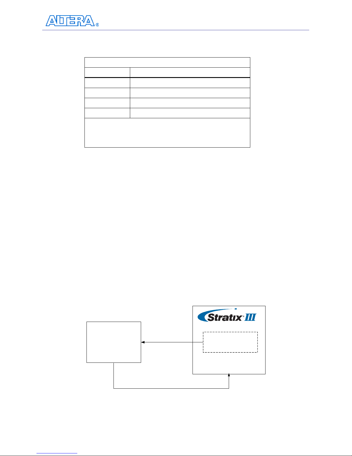
After the FPGA is programmed, the power controller IP will control the V
CCIO
control circuit to
provide desired V
CCIO
and V
CCPD
level to the FPGA, according to I/O standard selected by users as
indicated in Figure 2.10.With this feature, users can not only confirm if the V
CCIO
level meets the
design requirement, but also reduce the chance of the DE3 board and its daughter cards being
damaged.
Please refer to Stratix III handbook chapter 7. Stratix III Device I/O Features for more information
about the I/O standard and voltage levels of the Stratix III device. There will be more instructions
for DE3 System Builder in Chapter 4.
V
CCIO
Selection
Power Control
IP
V
CCIO
to I/O bank
V
CCIO
Voltage-Level
Control Circuit
Figure 2.10. The architecture of Power Control IP and V
CCIO
control circuit
Page 19
DE3 User Manual
16
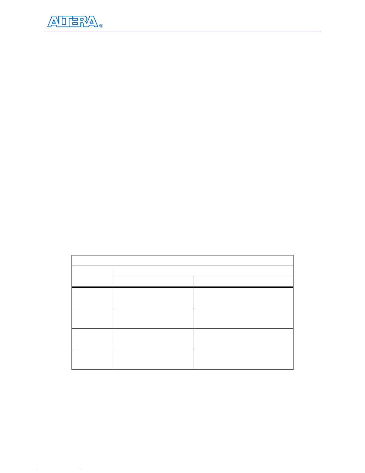
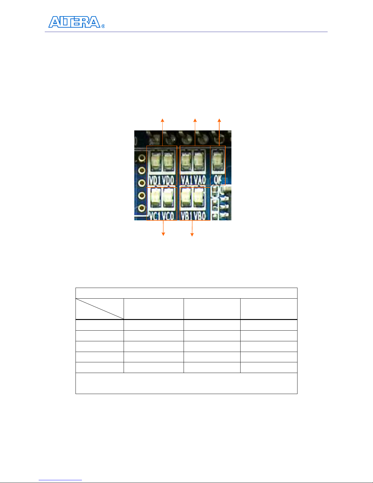
Finally, there are LEDs located at the left-top corner of the DE3 board to indicate the V
CCIO
voltage
level of each I/O group, as shown in Figure 2.11. For example, the LED VA1 and VA2 will be
turned on and off, respectively, when the V
CCIO
of I/O Group A is set to 2.5V. Please refer to Table
2-3 for the status of the LED indicator.
For I/O
Group A
For I/O
Group D
For I/O
Group C
For I/O
Group B
Power
ON/OFF
Indicator
Figure 2.11. The Voltage-Level Indicator for the I/O Groups
Table 2-3 The LEDs indicates the V
CCIO
voltage level of each IO Group.
LED
V
CCIO
Vx1(1) Vx0(1) OK
3.3V Light ON Light ON Light ON
2.5V Light ON Light OFF Light ON
1.8V Light OFF Light ON Light ON
1.5V Light OFF Light OFF Light ON
0V Light OFF Light OFF Light OFF
Note:
(1): Vx1 can be VA1, VB2, VC3, and VD1; Vx0 can be VA0, VB0, VC0, and VD0
Page 20

DE3 User Manual
17
2.5 Using the HSTC Connectors
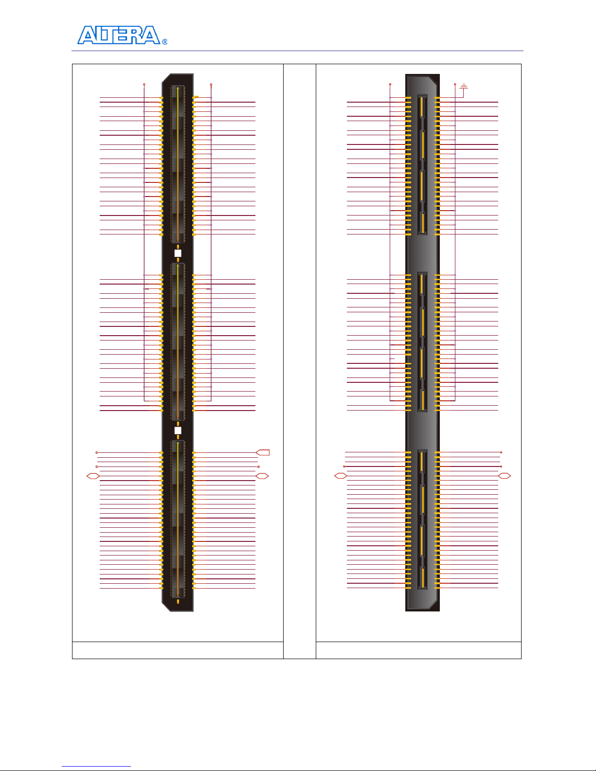
The High Speed Terasic Connector (HSTC) is a high speed expansion interface defined by Terasic
Technologies. The DE3 board is equipped with 8 HSTC connectors (J1 ~ J8), which can be used to
connect the Stratix III FPGA with daughter boards or the other DE3 boards. The detailed
specifications of the HSTC connector are described below:
4 HSTC Connector Groups:
The eight HSTC connectors on the DE3 board are divided into 4 groups: HSTC A, HSTC B,
HSTC C, and HSTC D. Each group has a male and female HSTC connector on the top and
bottom side of the DE3 board, respectively. In addition, both the male and female HSTC
connector shares the same I/O pins except JTAG and I2C interface.
I/O Distribution:
Each HSTC connector has 120 single-ended I/O (60 pair differential channels), 10
single-ended IO with 5 each for clock input and output (2 differential clock input and output
channel), JTAG and I2C bus. In addition, there are three banks on a HSTC connector. The I/O
pins used in differential transceiver channels on bank 1 support true LVDS inout. On bank 2
and 3, the I/O pins used in differential transmitter channels support emulated LVDS via a
termination resistor, and the differential receiver channels support true LVDS, as shown in.
Figure 2.12. In addition, there is a software utility named “DE3_HSTC” which can perform
the connection test between the I/O pins of the HSTC connector and Stratix III FPGA. The
detailed information about this utility can be found in Appendix D : DE3_HSTC Utility.
Configurable I/O Standards:
The I/O pins of the HSTC connector support many I/O standards with different voltage level,
as the V
CCIO
supplied to FPGA bank I/O is configurable. Users can choose the I/O standard of
HSTC connector in the software utility “DE3 System Builder”.
Compatible with HSMC Connector :
The HSTC connector is not only designed to be backward-compatible with the HSMC
products, but also provides more I/O pins for further connection. The pin assignments of bank
1 and 2 are exactly the same. The only difference between the HSMC and HSTC connector is
the pin assignments for bank 3. For HSTC connector, all the I/O pins on the bank 3 are well
defined. Figure 2.13 shows the I/O distribution of the bank3 for the HSTC and HSMC
connector. Table B-1 shows the pin compatible list for HSTC and HSMC connector.
Page 21
DE3 User Manual
18
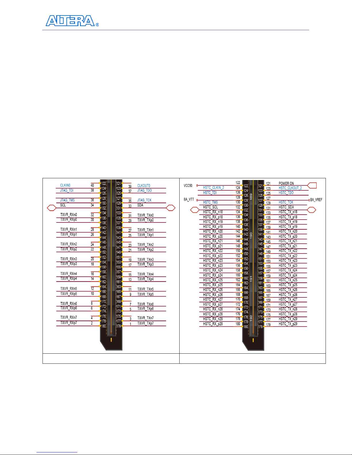
VCC50
BA_VREF
HSTC_CLKIN_n 0
GND
HSTC_CLKIN_p 0
HSTC_RX_n0
HSTC_RX_p0
HSTC_RX_n1
HSTC_RX_p1
HSTC_RX_n2
HSTC_RX_p2
HSTC_RX_n3
HSTC_RX_p3
HSTC_RX_n4
HSTC_RX_p4
HSTC_RX_n5
HSTC_RX_p5
HSTC_RX_n6
HSTC_RX_p6
HSTC_RX_n7
HSTC_RX_p7
HSTC_RX_n8
HSTC_RX_p8
HSTC_CLKIN_n 1
HSTC_CLKIN_p 1
HSTC_RX_n9
HSTC_RX_p9
HSTC_RX_n10
HSTC_RX_p10
HSTC_RX_n11
HSTC_RX_p11
HSTC_RX_n12
HSTC_RX_p12
HSTC_RX_n13
HSTC_RX_p13
HSTC_RX_n14
HSTC_RX_p14
HSTC_RX_n15
HSTC_RX_p15
HSTC_RX_n16
HSTC_RX_p16
HSTC_RX_n17
HSTC_RX_p17
HSTC_CLKIN_ 2
HSTC_TDI
HSTC_TMS
HSTC_SCL
HSTC_RX_n18
HSTC_RX_p18
HSTC_RX_n19
HSTC_RX_p19
HSTC_RX_n20
HSTC_RX_p20
HSTC_RX_n21
HSTC_RX_p21
HSTC_RX_n22
HSTC_RX_p22
HSTC_RX_n23
HSTC_RX_p23
HSTC_RX_n24
HSTC_RX_p24
HSTC_RX_n25
HSTC_RX_p25
HSTC_RX_n26
HSTC_RX_p26
HSTC_RX_n27
HSTC_RX_p27
HSTC_RX_n28
HSTC_RX_p28
HSTC_RX_n29
HSTC_RX_p29
2
4
6
8
10
12
14
16
18
20
22
24
26
28
30
32
34
36
38
40
42
44
46
48
50
52
54
56
58
60
64
66
70
72
62
68
76
78
74
82
84
80
88
90
86
94
96
92
100
102
98
106
108
104
112
114
110
118
120
122
124
126
128
130
132
134
136
138
140
142
144
146
148
150
152
154
156
158
160
162
164
166
168
170
172
174
176
178
180
116
1
3
5
7
9
11
13
15
17
18
21
23
25
27
39
31
33
35
37
39
41
43
45
47
49
51
53
55
57
59
63
65
69
71
61
67
75
77
73
81
83
79
87
89
85
93
95
91
99
101
97
105
107
103
111
113
109
117
119
121
123
125
127
129
131
133
135
137
139
141
143
145
147
149
151
153
155
157
159
161
163
165
167
169
171
173
175
177
179
115
1
3
5
7
9
11
13
15
17
19
21
23
25
27
29
31
33
35
37
39
41
43
45
47
49
51
53
55
57
59
63
65
69
71
61
67
75
77
73
81
83
79
87
89
85
93
95
91
99
101
97
105
107
103
111
113
109
117
119
121
123
125
127
129
131
133
135
137
139
141
143
145
147
149
151
153
155
157
159
161
163
165
167
169
171
173
175
177
179
115
VCC3312V
J
2
HSTC Connector A-Top (Male)
BA_VTT
HSTC_CLKOUT_n0
HSTC_CLKOUT_p0
HSTC_TX_n0
HSTC_TX_p0
HSTC_TX_n1
HSTC_TX_p1
HSTC_TX_n2
HSTC_TX_p2
HSTC_TX_n3
HSTC_TX_p3
HSTC_TX_n4
HSTC_TX_p4
HSTC_TX_n5
HSTC_TX_p5
HSTC_TX_n6
HSTC_TX_p6
HSTC_TX_n7
HSTC_TX_p7
HSTC_TX_n8
HSTC_TX_p8
HSTC_CLKOUT_n1
HSTC_CLKOUT_p1
HSTC_TX_n9
HSTC_TX_p9
HSTC_TX_n10
HSTC_TX_p10
HSTC_TX_n11
HSTC_TX_p11
HSTC_TX_n12
HSTC_TX_p12
HSTC_TX_n13
HSTC_TX_p13
HSTC_TX_n14
HSTC_TX_p14
HSTC_TX_n15
HSTC_TX_p15
HSTC_TX_n16
HSTC_TX_p16
HSTC_TX_n17
HSTC_TX_p17
HSTC_CLKOUT_2
POWER ON
HSTC_TDO
HSTC_TCK
HSTC_SDA
HSTC_TX_n18
HSTC_TX_p18
HSTC_TX_n19
HSTC_TX_p19
HSTC_TX_n20
HSTC_TX_p20
HSTC_TX_n21
HSTC_TX_p21
HSTC_TX_n22
HSTC_TX_p22
HSTC_TX_n23
HSTC_TX_p23
HSTC_TX_n24
HSTC_TX_p24
HSTC_TX_n25
HSTC_TX_p25
HSTC_TX_n26
HSTC_TX_p26
HSTC_TX_n27
HSTC_TX_p27
HSTC_TX_n28
HSTC_TX_p28
HSTC_TX_n29
HSTC_TX_p29
Bank
1
2
2
4
4 HSTCA_CL KIN_n0
HSTCA_CL KIN_p0
HSTCA_RX_n0
HSTCA_RX_p0
HSTCA_RX_n1
HSTCA_RX_p1
HSTCA_RX_n2
HSTCA_RX_p2
HSTCA_RX_n3
HSTCA_RX_p3
HSTCA_RX_n4
HSTCA_RX_p4
HSTCA_RX_n5
HSTCA_RX_p5
HSTCA_RX_n6
HSTCA_RX_p6
HSTCA_RX_n7
HSTCA_RX_p7
HSTCA_RX_n8
HSTCA_RX_p8
6
6
8
8
10
10
12
12
14
14
16
16
18
18
20
20
22
22
24
24
26
26
28
28
30
30
32
32
34
34
36
36
38
38
40
40
42
42
44
44
46
46
48
48
50
50
52
52
54
54
56
56
58
58
60
60
HSTCA_CLKIN_n1
64
64
HSTCA_CLKIN_p1
66
66
HSTCA_RX_n9
70
70
HSTCA_RX_p9
72
72
62
62
68
68
HSTCA_RX_n1 0
76
76
HSTCA_RX_p1 0
78
78
74
74
HSTCA_RX_n1 1
82
82
HSTCA_RX_p1 1
84
84
80
80
HSTCA_RX_n1 2
88
88
HSTCA_RX_p1 2
90
90
86
86
HSTCA_RX_n1 3
94
94
HSTCA_RX_p1 3
96
96
92
92
HSTCA_RX_n1 4
100
100
HSTCA_RX_p1 4
102
102
98
98
HSTCA_RX_n1 5
106
106
HSTCA_RX_p1 5
108
108
104
104
HSTCA_RX_n1 6
112
112
HSTCA_RX_p1 6
114
114
110
110
HSTCA_RX_n1 7
118
118
HSTCA_RX_p1 7
120
120
122
122
HSTCA_CLKIN_2
VCC50
BA_VTT
124
124
124
HSTCA_TDI
HSTCA_TMS
126
126
128
128
130
130
HSTCA_SCL
132
132
HSTCA_RX_n1 8
134
134
HSTCA_RX_p1 8
136
136
HSTCA_RX_n1 9
138
138
HSTCA_RX_p1 9
140
140
HSTCA_RX_n2 0
142
142
HSTCA_RX_p2 0
144
144
HSTCA_RX_n2 1
146
146
HSTCA_RX_p2 1
148
148
HSTCA_RX_n2 2
150
150
HSTCA_RX_p2 2
152
152
HSTCA_RX_n2 3
154
154
HSTCA_RX_p2 3
156
156
HSTCA_RX_n2 4
158
158
HSTCA_RX_p2 4
160
160
HSTCA_RX_n2 5
162
162
HSTCA_RX_p2 5
164
164
HSTCA_RX_n2 6
166
166
HSTCA_RX_p2 6
168
168
HSTCA_RX_n2 7
170
170
HSTCA_RX_p2 7
172
172
HSTCA_RX_n2 8
174
174
HSTCA_RX_p2 8
176
176
HSTCA_RX_n2 9
178
178
HSTCA_RX_p2 9
180
180
116
116
1
3
5
7
9
11
13
15
17
19
21
23
25
27
29
31
33
35
37
39
41
43
45
47
49
51
53
55
57
59
63
65
69
71
61
67
75
77
73
81
83
79
87
89
85
93
95
91
99
101
97
105
107
103
111
113
109
117
119
121
123
125
127
129
131
133
135
137
139
141
143
145
147
149
151
153
155
157
159
161
163
165
167
169
171
173
175
177
179
115
HSTCA_CLKOUT_n0
VCC33 12V
J1
HSTC Connector A-Bottom (Female)
HSTCA_CLKOUT_p0
HSTCA_TX_n0
HSTCA_TX_p0
HSTCA_TX_n1
HSTCA_TX_p1
HSTCA_TX_n2
HSTCA_TX_p2
HSTCA_TX_n3
HSTCA_TX_p3
HSTCA_TX_n4
HSTCA_TX_p4
HSTCA_TX_n5
HSTCA_TX_p5
HSTCA_TX_n6
HSTCA_TX_p6
HSTCA_TX_n7
HSTCA_TX_p7
HSTCA_TX_n8
HSTCA_TX_p8
HSTCA_CLKOUT_n1
HSTCA_CLKOUT_p1
HSTCA_TX_n9
HSTCA_TX_p9
HSTCA_TX_n10
HSTCA_TX_p10
HSTCA_TX_n11
HSTCA_TX_p11
HSTCA_TX_n12
HSTCA_TX_p12
HSTCA_TX_n13
HSTCA_TX_p13
HSTCA_TX_n14
HSTCA_TX_p14
HSTCA_TX_n15
HSTCA_TX_p15
HSTCA_TX_n16
HSTCA_TX_p16
HSTCA_TX_n17
HSTCA_TX_p17
HSTCA_CLKOUT_2
POWER ON
BA_VREF
HSTCA_TDO
HSTCA_TCK
HSTCA_SDA
HSTCA_TX_n18
HSTCA_TX_p18
HSTCA_TX_n19
HSTCA_TX_p19
HSTCA_TX_n20
HSTCA_TX_p20
HSTCA_TX_n21
HSTCA_TX_p21
HSTCA_TX_n22
HSTCA_TX_p22
HSTCA_TX_n23
HSTCA_TX_p23
HSTCA_TX_n24
HSTCA_TX_p24
HSTCA_TX_n25
HSTCA_TX_p25
HSTCA_TX_n26
HSTCA_TX_p26
HSTCA_TX_n27
HSTCA_TX_p27
HSTCA_TX_n28
HSTCA_TX_p28
HSTCA_TX_n29
HSTCA_TX_p29
Bank
2
Bank
3
Male HSTC connector Female HSTC connector
Figure 2.12. The male and female HSTC connectors
Page 22
DE3 User Manual
19
Share the same I/O pins with other connectors:
The HSTC connector group HSTCA (J1, J2) and HSTCB (J3, J4) share the same I/O pins with
the GPIO expansion headers (J13, J14) and DDR2 SO-DIMM socket (J9), respectively. Hence
none of the combinations above is allowed to be used at the same time.
Power Supply:
The HSTC connector provides 12, 5, and 3.3 volt for power supply purpose. There are also two
power input pin named B<HSTC Group>_VTT and B<HSTC Group>_VREF, which are
connected to the input reference voltage(V
REF
) and termination voltage pin (VTT) of the Stratix
III FPGA, respectively.
Finally, Table A-6 to Table A-11 shows the connections between the HSTC connectors and the
FPGA.
HSMC HSTC
Figure 2.13. The difference between the HSMC and HSTC connectors
Page 23

DE3 User Manual
20
2.6 Connecting HSTC/HSMC Daughter Boards to DE3 HSTC
connectors
It is important when the HSTC/HSMC daughter boards are connected to the DE3 HSTC connector
is to ensure the I/O pins are properly matched between the daughter board and the DE3 connector in
particular the 12V, 5V, and 3.3V power pins. If there are mismatch in pins between the two
connectors, not only would it cause damage to the daughter board but more importantly the FPGA
itself. Please note daughter boards can only be connected to the TOP HSTC connector of the DE3
board, therefore the bottom HSTC connector are only used to establish connection for stacking
purposes.
2.7 Using the GPIO Expansion Headers
The DE3 Board provides two 40-pin expansion headers as shown in Figure 2.14. Each header has
36 pins connected to the Stratix III FPGA, and the two headers share the same I/O pins with HSTC
connector A. The other 4 pins provide DC +5V (VCC5), DC +3.3V (VCC33), and two GND pins.
Among these 36 I/O pins, there are 4 pins connected to the PLL clock input and output pins of the
FPGA.
The I/O pins on the expansion headers have a great flexibility in selecting the I/O standards. The
voltage level of the V
CCIO
can be configured as 3.3V, 2.5V, 1.8V, or 1.5V.
Finally, Figure 2.15 shows the connections between the GPIO expansion headers and Stratix III.
The pin assignments are given in Table A-12 and Table A-13.
Page 24
DE3 User Manual
21
1
3
5
7
9
11
13
15
17
19
21
23
25
27
29
31
33
35
37
39
2
4
6
8
10
12
14
16
18
20
22
24
26
28
30
32
34
36
38
40
GPIO0_CLKINn0
GPIO0_CLKINp0
GPIO0_D2
GPIO0_D4
GPIO0_D6
5V
GPIO0_D8
GPIO0_D10
GPIO0_D12
GPIO0_CLKOUTn0
GPIO0_CLKOUTp0
GPIO0_D16
GPIO0_D18
GPIO0_D20
3.3V
GPIO0_D22
GPIO0_D24
GPIO0_D26
GPIO0_D28
GPIO0_D30
GPIO0_D0
GPIO0_D1
GPIO0_D3
GPIO0_D5
GPIO0_D7
GND
GPIO0_D9
GPIO0_D11
GPIO0_D13
GPIO0_D14
GPIO0_D15
GPIO0_D17
GPIO0_D19
GPIO0_D21
GND
GPIO0_D23
GPIO0_D25
GPIO0_D27
GPIO0_D29
GPIO0_D31
J13
GPIO 0
1
3
5
7
9
11
13
15
17
19
21
23
25
27
29
31
33
35
37
39
2
4
6
8
10
12
14
16
18
20
22
24
26
28
30
32
34
36
38
40
GPIO1_CLKINn1
GPIO1_CLKINp1
GPIO1_D2
GPIO1_D4
GPIO1_D6
5V
GPIO1_D8
GPIO1_D10
GPIO1_D12
GPIO1_CLKOUTn1
GPIO1_CLKOUTp1
GPIO1_D16
GPIO1_D18
GPIO1_D20
3.3V
GPIO1_D22
GPIO1_D24
GPIO1_D26
GPIO1_D28
GPIO1_D30
GPIO1_D0
GPIO1_D1
GPIO1_D3
GPIO1_D5
GPIO1_D7
GND
GPIO1_D9
GPIO1_D11
GPIO1_D13
GPIO1_D14
GPIO1_D15
GPIO1_D17
GPIO1_D19
GPIO1_D21
GND
GPIO1_D23
GPIO1_D25
GPIO1_D27
GPIO1_D29
GPIO1_D31
J14
GPIO 1
Figure 2.14. Pin distribution of the GPIO expansion headers
1
3
19
AD19
AE32
AE31
AE18
GPIO 0
GPIO 1
CLKOUTn0
CLKOUTp0
CLKINn0
CLKINp0
AE19
AD18
AP19
AN19
21
CLKOUTn1
CLKOUTp1
CLKINn1
CLKINp1
1
3
19
21
GPIO0_D [ 0 .. 31 ]
RX_n [ 0 .. 15 ]
RX_p [ 0 .. 15 ]
TX_n [ 0 .. 15 ]
TX_p [ 0 .. 15 ]
GPIO1_D [ 0 .. 31 ]
HSTC A
See Table A-12,13
CLKOUTn0
CLKOUTp0
CLKINn0
CLKINp0
CLKOUTn1
CLKOUTp1
CLKINn1
CLKINp1
See Table A-12,13
See Table A-12,13
See Table A-12,13
Figure 2.15. Connections between the GPIO expansion headers and Stratix III
2.8 Using the DDR2 SO-DIMM
The DE3 board provides a 200-pin DDR2 SO-DIMM socket. The maximum capacity supported is
4GB. The DDR2 SO-DIMM shares the same I/O pins with the HSTC connector B, except the
Page 25
DE3 User Manual
22
command input signals DDR2_CS_N[1..0] and presence-detect address input signals
DDR2_SA[1..0]. Users should never use the DDR2 SO-DIMM socket and the HSTC connector B at
the same time.
Figure 2.16 shows the connections between the DDR2 SO-DIMM socket and Stratix
III device. The pin assignments are listed in Table A-14.
T8
T9
DDR2_DQ [ 0..63 ]
HSTCB_SCL
HSTCB_SDA
HSTCB_RX_n [ 0 .. 29 ]
HSTCB_RX_p [ 0 .. 29 ]
HSTCB_TX_n [ 0 .. 29 ]
HSTCB_TX_p [ 0 .. 29 ]
DDR2_DQS_p [ 0..7 ]
DDR2_DQS_n [ 0..7 ]
DDR2_A [ 0..15 ]
DDR2_DM [ 0..7 ]
DDR2_CLK_p [ 0..1 ]
DDR2_CLK_n [ 0..1 ]
DDR2_BA [ 0..2 ]
DDR2_ODT [ 0..1 ]
DDR2_CKE [ 0..1 ]
DDR2_CS_n [ 0..1 ]
DDR2_SCL
DDR2_SDA
HSTC B
DDR2_CS_n [ 0..1 ]
DDR2_SA [ 0..1 ]
Figure 2.16. Connections between the DDR2 and Stratix III FPGA
2.9 Using the USB OTG
The DE3 board provides both USB host and device interfaces using the Philips ISP1761ET
single-chip USB controller. The host and device controllers are compliant with the Universal Serial
Bus Specification Rev. 2.0, supporting data transfer at high-speed (480 Mbit/s), full-speed (12
Mbit/s) and low-speed (1.5 Mbit/s). Figure 2.17 shows the connection between the USB OTG and
Stratix III device. The port 1 can be configured as a downstream port, or an upstream port or OTG
port. If the port 1 is configured as an OTG port, users can use JP1 to specify host or peripheral role,
as listed in Table 2-4. The pin assignments for the associated interface are listed in Table A-15.
Page 26
DE3 User Manual
23
NXP
ISP1761ET
DM1
DP1
USB_ID
DM2
DM3
DP2
DP3
miniAB
TYPE A
JP1 Close = Host
JP1 Open = Device
Host
TYPE A
Host
A[ 1..17]
D[ 0..31]
CS
WR
RD
RESET
HC_IRQ
DC_IRQ
HC_DREQ
HC_DACK
DC_DREQ
DC_DACK
CLKIN
P28
N29
N30
P29
R27
T23
R28
R25
R26
R24
See Table A-15
12MHz
See Table A-15
Figure 2.17. Connections between the USB OTG and Stratix III device
Detailed information of the ISP1761ET device can be found in its datasheet and programming guide;
both documents are available from the manufacturer’s web site, or in the Datasheet/USB folder of
the DE3 System CD. Two complete examples for host and device applications each, can be found
in Sections 5.1and 5.2. These demonstrations provide software drivers for the Nios II processor.
Table 2-4 The default host or peripheral setting for port 1 (J15) of the
ISP1761ET
JP1 setting Connectors
Open Port1 set to peripheral
Close Port 1 set to host
2.10 Using the SD Card
The DE3 board has a SD card socket and can be accessed as optional external memory in both SPI
and 1-bit SD mode. Table A-16 shows the pinout of the SD card socket with Stratix III FPGA.
5
R10
SD Card
SD_CMD
P8
N5
P7
2
7
11
SD_CLK
SD_WPn
SD_DAT 0
Page 27
DE3 User Manual
24
Figure 2.18. Connections between the SD card and Stratix III
2.11 LED Indicators
The DE3 board includes some LEDs to indicate the specified hardware status. The relationship of
LED names and their associated functions are list in Table 2-5.
Table 2-5 Description for LED indicator
LED Name Descriptions
POWER Light on when Power switch(SW5) is turned on
CONF_DONE
Light on when the configuration data is received by Stratix
III FPGA without error ad initialization cycle starts.
LOAD Light on when USB blaster circuit transmits or receives data
LINKA
Light on when HSTC connector A top (J1) is connected with
an extended board
LINKB
Light on when HSTC connector B top (J3) is connected with
an extended board
LINKC
Light on when HSTC connector C top (J5) is connected with
an extended board
LINKD
Light on when HSTC connector D top (J7) is connected with
an extended board
OVT
Light on when the temperature value of the FPGA is higher
than the threshold value setting in the temperature sensor.
USB3,
USB2,
USB1
Power LED indicators for USB port3 (J17), port2 (J16), and
port1 (J1). Each LED will be on as soon as the port power of
the respective port is enabled by software, for example,
after loading drivers
2.12 Clock Circuitry
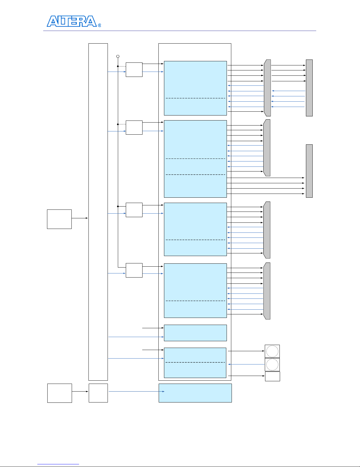
Clock inputs:
The clock input source of Stratix III FPGA comes from the clock buffer, HSTC connectors, GPIO
expansion headers, and SMA connector as indicated in Figure 2.19. Three of five clock inputs are
connected to the dedicated high speed clock input pins of the FPGA, which allows users to use any
of these clocks as a source clock for the PLL circuit.
Note: The 3 clock inputs connected to the dedicated inputs of the FPGA are (CLKIN_2, CLKIN_n1,
and CLKIN_p1 respectively).
Clock outputs:
Page 28

DE3 User Manual
25
The clock output of Stratix III FPGA includes HSTC connectors, GPIO expansion headers, SMA
connector, and SD card socket as shown in
Figure 2.19.
The associated pin assignments for clock buffer and SMA connectors to FPGA I/O pins are shown
in Table A-17.
Page 29
DE3 User Manual
26
50MHz
Oscillator
Adjustable
+3.3V
Level
Shift
Adjustable
Adjustable
Adjustable
+3.3V
+3.3V
50MHz
50MHz
VCCIO
CLK4p
50MHz
50MHz
50MHz
USB
Blaster
Circuit
12MHz
USB 2.0 OTG
CLK4n
HSTC A
CLKIN2
CLK5n
CLKIN_n1
CLK5p
CLKIN_p1
CLKIN_n1
CLKIN_p1
GPIO
CLKOUT_n1
CLKOUT_p1
PLL_B1_CLKOUT4
Bank 3C
Bank 2A
CLKIN_n0
CLKIN_p0
CLKIN_n0
CLKIN_p0
CLKOUT2
DIFFIO_RX_L34n
DIFFIO_RX_L34p
DIFFIO_TX_L33p
VCCIO
CLK6p
CLK6n
CLK7n
CLK7p
PLL_B2_CLKOUT4
Bank 4C
Bank 5A
DIFFIO_RX_R11n
DIFFIO_RX_R11p
DIFFIO_TX_R12p
DDR2
Bank 4A
DIFFIO_RX_B47n
DIFFOUT_B94n
VCCIO
CLK12p
CLK12n
CLK13n
CLK13p
PLL_T2_CLKOUT4
Bank 7C
Bank 6A
DIFFIO_RX_R34n
DIFFIO_RX_R34p
DIFFIO_TX_R33p
VCCIO
CLK14p
CLK14n
CLK15n
CLK15p
PLL_T1_CLKOUT4
Bank 8C
Bank 1A
DIFFIO_RX_L11n
DIFFIO_RX_L11p
DIFFIO_TX_L12p
Level
Shift
Level
Shift
Level
Shift
VCCIO
Bank 1C
CLK1p
VCCIO
Bank 5C
Bank 6C
CLK8p
CLK10p
EXT_CLK
SMA
CLK_OUT
PLL_R3_FB_CLKOUT0p
SMA
24MHz
Oscillator
High
Speed
Clock
Buffer
PLL_T1_CLKOUT3
PLL_T1_CLKOUT0n
PLL_T1_CLKOUT0p
PLL_T2_CLKOUT3
PLL_T2_CLKOUT0n
PLL_T2_CLKOUT0p
PLL_B2_CLKOUT3
PLL_B2_CLKOUT0n
PLL_B2_CLKOUT0p
PLL_B1_CLKOUT3
PLL_B1_CLKOUT0n
PLL_B1_CLKOUT0p
CLKOUT_n0
CLKOUT_p0
CLKOUT_n1
CLKOUT_p1
CLKOUT_n0
CLKOUT_p0
HSTC B
CLKIN2
CLKIN_n1
CLKIN_p1
CLKOUT_n1
CLKOUT_p1
CLKIN_n0
CLKIN_p0
CLKOUT2
CLKOUT_n0
CLKOUT_p0
DIFFIO_RX_B47p
DIFFOUT_B94p
DDR2_CLKn0
DDR2_CLKp1
DDR2_CLKn1
DDR2_CLKp1
HSTC C
CLKIN2
CLKIN_n1
CLKIN_p1
CLKOUT_n1
CLKOUT_p1
CLKIN_n0
CLKIN_p0
CLKOUT2
CLKOUT_n0
CLKOUT_p0
HSTC D
CLKIN2
CLKIN_n1
CLKIN_p1
CLKOUT_n1
CLKOUT_p1
CLKIN_n0
CLKIN_p0
CLKOUT2
CLKOUT_n0
CLKOUT_p0
50MHz
SD
card
SD_CLK
DIFFIO_TX_R31p
OSC_BA
OSC_BB
OSC_BC
OSC_BD
OSC1_50
OSC2_50
Stratix III
Figure 2.19. Clock connections of the DE3
Page 30
DE3 User Manual
27
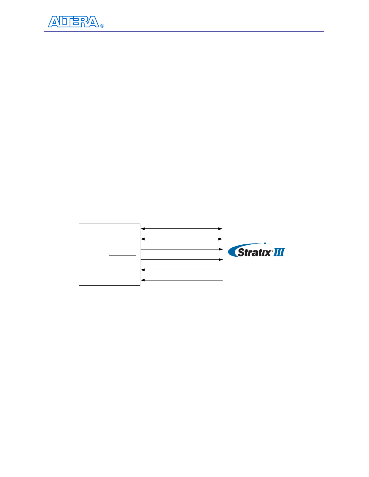
2.13 Using the Temperature Sensor
The DE3 board is equipped with a temperature sensor MAX1619, which provides temperature
sensing and over-temperature alert. These functions are achieved by connecting the temperature
sensor to the internal temperature sensing diode of the Stratix III device. The temperature status and
alarm threshold registers of the temperature sensor can be programmed by a two-wire SMBus,
which is connected to the Stratix III FPGA as shown in Figure 2.20. In addition, the 7-bit POR slave
address for this sensor is set to ‘0011000’.
There is an option of connecting a 2-pin +12V fan to JP2 for cooling purpose. The pin near the
HSTC connector C is for +12V, the other one is used for GND. When the temperature of the FPGA
device is over the threshold value set by users, the fan will be turned on. The pin assignments for
the associated interface are listed in Table A-18.
Finally, the detailed information of the temperature sensor device can be found in its datasheet,
which is available from the manufacturer’s web site, or in the Datasheet/Temperature_Sensor folder
of the DE3 System CD.
TEMP_CLK
TEMP_DATA
TEMP_INTn
TEMP_OVERn
Temperature
Sensor
TEMPDIODEp
TEMPDIODEn
DXP
DXN
ALERT
OVERT
SMBDATA
SMBCLK
Figure 2.20. Connections between the temperature sensor and Stratix III device
Page 31

DE3 User Manual
28
Chapter 3
Control Panel
3
The DE3 board comes with a PC-based Control Panel that allows users to access various
components onboard. The host computer communicates with the board via USB port. The tool can
be used to verify the functionality of components.
This chapter presents some basic functions of the Control Panel, illustrates its structure in block
diagram form, and finally describes its capabilities.
3.1 Control Panel Setup
The Control Panel software utility is located in the directory “/Tools/DE3_control_panel” in the
DE3 System CD. To execute the program, simply copy the whole folder to your host computer and
launch the control panel by double clicking the “DE3_Control_Panel.exe”.
The DE3_Control_Panel.exe will auto-detect the FPGA and download the control codes, the .sof
and .elf file, to the Stratix III device through USB-Blaster port.
To activate the Control Panel, perform the following steps:
1. Make sure Quartus II and NIOS II are installed successfully on your PC.
2. Connect the supplied USB cable to the USB Blaster port and the supplied power cord to
J18. Turn the power switch ON as shown in Figure 3.1.
3. Start the executable DE3_control_panel.exe on the host computer. Figure 3.2 will appear
and the Control Panel starts to auto-detect the FPGA and download the .sof and .elf files.
4. After the configuration file is programmed to the DE3 board, the FPGA device information
will be displayed on the window.
5. Note the Control Panel will occupy the USB port, users will not be able to download any
configuration file into the FPGA before you exit the Control Panel program.
6. The Control Panel is now ready, as shown in Figure 3.3
Page 32

DE3 User Manual
29
Figure 3.1. Setup of USB-Blaster cable and power cord
Figure 3.2. Download .sof and .elf files to the DE3 board
Page 33

DE3 User Manual
30
Figure 3.3. DE3 Control Panel is ready
If the connection between DE3 board and USB-Blaster is not established, or the DE3 board is not
powered on before running the DE3_control_panel.exe, the Control Panel will fail to detect the
FPGA and a warning message window will pop up as shown in Figure 3.4.
Figure 3.4. The DE3 Control Panel fails to download .sof file
Page 34

DE3 User Manual
31
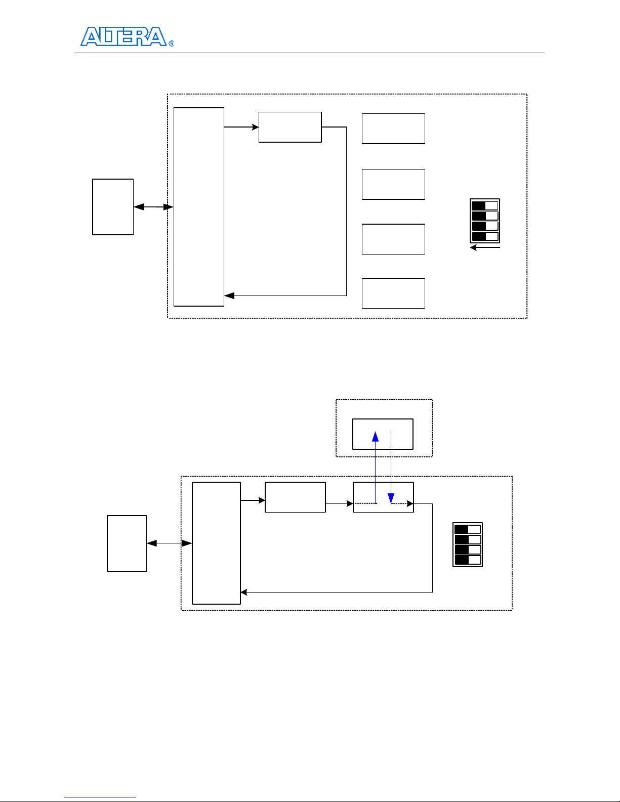
The concept of the DE3 Control Panel is illustrated in
Figure 3.5.The “Control Codes” which
performs the control functions is implemented in the FPGA board. It communicates with the
Control Panel window, which is active on the host computer, via the USB Blaster link. The
graphical users interface is used to issue commands to the control codes. It handles all requests and
performs data transfer between the computer and the DE3 board.
EPCS
128
Control
Codes
IO BANK POWER
Power Off / Write / Read
Figure 3.5. The DE3 Control Panel concept
The DE3 Control Panel can be used to light up LEDs, change the values displayed on 7-segment
displays, monitoring buttons/switches status, read/write the serial configuration devices (EPCS128),
access DDR2 SO-DIMM memory, read the information of SD Card, and setup the V
CCIO
level of
the I/O Groups.
3.2 Controlling the LEDs and 7-Segment Displays
One of the functions of the Control Panel is to set up the status of the LEDs and 7-segment displays.
The tab-window shown in Figure 3.6 indicates where you can directly turn all the LEDs on or off
individually by selecting them and clicking “Light All” or “Unlight All”.
Page 35

DE3 User Manual
32
Figure 3.6. Controlling LEDs
Figure 3.7 shows the interface of the 7-SEG and how to select desired patterns. The status of the
7-SEG patterns will be updated immediately.
Figure 3.7. Controlling 7-SEG display
Page 36

DE3 User Manual
33
3.3 SWITCH/BUTTON
Choose the Button tab as shown in Figure 3.8. This function is designed to monitor status of
switches and buttons from a graphic interface in real-time. It can be used to verify the functionality
of switches and buttons.
Figure 3.8. Monitoring Switches and Buttons
3.4 Memory Controller
The Control Panel can be used to write/read data to/from the DDR2 SO-DIMM memory on the DE3
board. We will describe how the DDR2 SO-DIMM is accessed. Click on the Memory tab to reach
the tab-window shown in Figure 3.9.
A 16-bit string can be written into the DDR2 SO-DIMM memory by three steps, namely specifying
the address of the desired location, entering the data to be written, and pressing the Write button.
Contents of the location can be read by pressing the Read button. Figure 3.10 depicts the result of
writing the hexadecimal value 7EFF to location 0x100, followed by reading the same location.
The Sequential Write function of the Control Panel is used to write the contents of a file to the serial
configuration device, as described below:
1. Specify the starting address in the Address box.
Page 37

DE3 User Manual
34
2. Specify the number of bytes to be written in the Length box. If the entire file is to be
loaded, a check mark can be placed in the File Length box instead of giving the number of
bytes.
3. To initiate the writing of data, click on the Write a File to Memory button.
4. When the Control Panel responds with the standard Windows dialog box asking for the
source file, specify the desired file in the usual manner.
The Sequential Read function is used to read the contents of the serial configuration device and
place them into a file as follows:
1. Specify the starting address in the Address box.
2. Specify the number of bytes to be copied into a file in the Length box. If the entire
contents of the serial configuration device are to be copied, then place a check mark in the
Entire Memory box.
3. Press Load Memory Content to a File button.
4. When the Control Panel responds with the standard Windows dialog box ask for the
destination file, users can specify the desired file in the usual manner.
Figure 3.9. Access DDR2 SO-DIMM memory
Page 38

DE3 User Manual
35
Figure 3.10. Writing the hexadecimal value 7EFF to location 0x100
3.5 USB2.0 OTG
Choose the USB tab to reach the window in Figure 3.11. The function is designed to monitor the
status of USB Hub in real-time.
Plug a USB device to any USB port of FPGA board, and both the device type and speed will be
displayed on the control window. Figure 3.11 shows a low-speed HID USB Mouse is plugged into
port 3.
Page 39

DE3 User Manual
36
Figure 3.11. Monitoring status of USB ports
3.6 SD CARD
Choose the SD-CARD tab to the window shown in Figure 3.12. The function is designed to read
the identification and specification of SD Card. Single-bit SD-MODE is used to access the SD Card.
This function can be used to verify the functionality of SD-CARD interface.
To gather the information, simply insert a SD Card to the FPGA board and press the Read button.
The SD-CARD identification and specification will be displayed on the control window
Page 40

DE3 User Manual
37
Figure 3.12. Reading the SD Card Identification and Specification
3.7 Temperature Monitor
Choose the Temperature tab to reach the window shown in Figure 3.13. The function is designed
to control temperature sensor through Control Panel. The temperatures of Stratix III and DE3 board
are shown on the right-hand side of the Control Panel.
When the temperature of Stratix III exceeds the Maximum setting of Over Temperature or Alert, a
warning message will be shown on the Control Panel. Click “Read” button to get current settings
for Over temperature and Alert. Users can enter the maximum and minimum temperatures for Over
temperature or Alert as required. Click the “Write” button to update the values entered.
Page 41

DE3 User Manual
38
Figure 3.13. Accessing the Temperature Sensor through Control Panel
3.8 I/O Group
Choose the I/O Group tab to reach the window shown in Figure 3.14. The function is designed to
read/write and control the V
CCIO
level of all I/O Groups of the DE3 board.
Click the “Read” button to enter the window shown in Figure 3.15. Current V
CCIO
level of all I/O
Groups will be displayed.
Page 42

DE3 User Manual
39
Figure 3.14. Accessing the power status of all I/O Groups
Figure 3.15. Reading the V
CCIO
level of all I/O Groups
Page 43

DE3 User Manual
40
3.9 Overall Structure of the DE3 Control Panel
The DE3 Control Panel communicates with control codes, which are instantiated in the Stratix III
FPGA..
To run the Control Panel, users must set it up first, as explained in Section 3.1. Figure 3.16 depicts
the structure of the Control Panel. Each input/output device is controlled by the NIOS II Processor
instantiated in the FPGA chip. The communication with the PC is done via the USB Blaster link.
The NIOS II interprets the commands sent from the PC and performs the appropriate actions.
Figure 3.16. The block diagram of the DE3 control panel
Page 44

DE3 User Manual
41
Chapter 4
DE3 System Builder
4
This chapter describes how to create a custom design project on the DE3 board by using DE3
System Builder.
4.1 Introduction
The DE3 System Builder is designed to assist users to create a Quartus II project for DE3 board
within minutes. The generated Quartus II project files include:
Quartus II Project File (.qpf)
Quartus II Setting File (.qsf)
Top-Level Deign File (.v)
Synopsis Design Constraints file (.sdc)
Encrypted Power Configuration Controller (.v)
Pin Assignment Document (.htm)
The DE3 System Builder not only can generate the files above, but also can provide error-checking
rules to prevent users from making the following common mistakes:
1. Board damaged for wrong pin/bank voltage assignment.
2. Board malfunction caused by wrong device connections or missing pin counts for
connected ends.
3. Performance dropped because of improper pin assignments.
4.2 General Design Flow
This section will introduce the general design flow to build a project for the DE3 board via the DE3
System Builder. The general design flow is illustrated in the Figure 4.1.
First of all, users should launch DE3 System Builder and create a new project according to the
requirement. When users complete the settings, the DE3 System Builder will generate three major
files, which include top-level deign file (.v), encrypted power configuration controller (.v), and
Quartus II setting file (.qsf).
Page 45

DE3 User Manual
42
The top-level deign file contains top-level verilog wrapper for users to add their own design/logic.
The encrypted power configuration controller file contains encrypted core which is generated by
user’s selection on I/O Group voltage. The Quartus II setting file contains information such as
FPGA device type, top-level pin assignment, and I/O standard for each user-defined I/O pin.
Next, users must be aware that they can never modify encrypted power configuration controller file.
User’s own design should be included within top-level deign file.
Finally, Quartus II programmer must be used to download SOF file to DE3 board using JTAG
interface.
Start
Launch
DE3 System Builder
Create New
DE3 System Builder
Project
.QPF
.QSF
.V
.HTML
.SDC
Generate
Quartuss II Project
and Document
Launch Quartus II and
Open Project
Add User Design/
Logic
Compile to generate
.SOF
Configure FPGA
End
Figure 4.1. The general design flow of building a design
for the DE3 board via the DE3 System Builder
Page 46

DE3 User Manual
43
4.3 Using DE3 System Builder
This section provides the detail procedures on how to use the DE3 System Builder.
Install and active the DE3 System Builder
The DE3 System Builder is located in the directory: "Tools\DE3_System_Builder" in
the DE3 System CD. Users can copy the whole folder to a host computer without
installing the utility. Before using the DE3 System Builder, perform the following steps:
Make sure the license file of the “Encrypted Power Configuration Controller
IP” is set in the Quartus II software. (Please refer to the section Add the License
File for Terasic Power Controller IP in the document named “Getting start with
Altera DE3 board” for more information on how to import a license file.)
Execute DE3_System_Builder.exe on the host computer. The DE3 System Builder
user-interface will appear, as shown in Figure 4.2.
Figure 4.2. The DE3 System Builder window
Add Board
On the left-hand side of the DE3 System Builder, there are many boards’ icons in the
Board Selection field. If users select a DE3 board and click Add button, a DE3
Configuration window will pop up. After the setting is completed, a DE3 board will be
added to the System Configuration field.
Page 47

DE3 User Manual
44
If users select any of the daughter boards in the Board Selection field, a window will
pop up and allow users to change the name of the daughter board. Click OK to add the
daughter board to System Configuration Filed.
DE3 Configuration
When users add a DE3 board, a DE3 Configuration window will pop up as shown in
Figure 4.3. This window allows users to configure many features for the DE3 board as
described below:
Figure 4.3. The DE3 Configuration window
Board Name: The board name will be set as the Quartus II project name when it is
created by DE3 System Builder.
FPGA Type: The FPGA device on DE3 board may be EP3SL150 or EP3SH340.
Users need to select the FPGA device and speed grade accordingly.
User I/O Components: Users can enable or disable the User I/O Component from
this field. If the User I/O component is enabled, the DE3 System Builder will
generate the port name, port connection rules (input/output) and the pin
assignments for the User I/O component on the Quartus II top-level file.
Page 48

DE3 User Manual
45
IO Group: There are four I/O Groups in the DE3 Configuration window. The
HSTC connector A, B, C, and D correspond to I/O Groups A, B, C, and D on DE3
board, respectively. Disabled I/O Groups will not be listed in the Quartus II
top-level file. There are three options for each I/O Group as listed below:
i. Type: Users can select a connector type for I/O Group A and B., as
the HSTC connector A and B share the same I/O bus with the GPIO
expansion headers and DDRII SO-DIMM socket.
ii. I/O standard: Users can select the I/O standard for the I/O Group.
iii. Name: Users can change the name of a connector.
I/O GROUP Voltage-level Indicator: This function will indicate the V
CCIO
level
for current I/O standard setting of the four I/O Croups. The status is same as the
LEDs on the DE3 board. Please refer to Section 2.4 for details.
Connection Between Two Connectors
When users add a DE3 board and daughter board in the System configuration field, it is
necessary to establish the connection in between. The port name, port connection rules
(input/output) and the pin assignment of the connector in the top-level file will be fully
compatible with this daughter board. The detailed steps for the connection setup are
shown below:
Establish and remove a connection between two connectors:
i. Move the mouse cursor to the upper connector as shown in Figure 4.4.
Figure 4.4. Step 1 of establishing a connection.
ii. Hold the left button of the mouse and Drag the mouse cursor to the
lower connector as shown in Figure 4.5.
Page 49

DE3 User Manual
46
Figure 4.5. Step 2 of establishing a connection
iii. Release the left mouse button and a green connection line will be
drawn between two connectors as shown in Figure 4.6.
Figure 4.6. Step 3 of establishing a connection
iv. Redo the steps i to iii will remove an established connection as shown
in Figure 4.7.
Figure 4.7. The step for removing a connection between two connectors
Warning message of an incorrect connection
If users try to establish a connection between two different types and I/O standard
of connectors, a warning message box will pop up as shown in Figure 4.8.
Page 50
DE3 User Manual
47
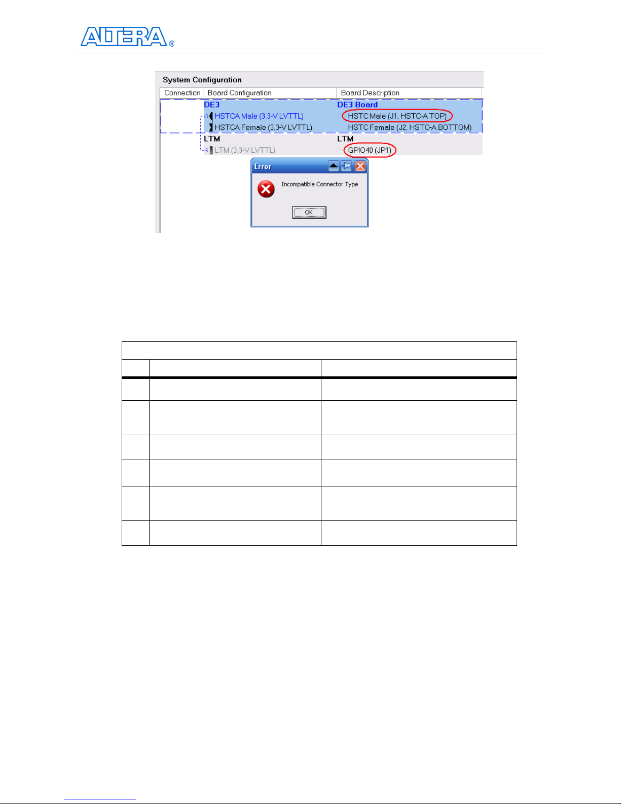
Figure 4.8. The error message box of an incorrect connection
Project Generation
When users press the Generate button, the DE3 System Builder will generate the
corresponding Quartus II files and documents as listed in the Table 4-1:
Table 4-1. The files generated by DE3 System Builder
No.
Filename Description
1 <Board name>.v Top level verilog file for Quartus II
2 IOV_<IO Group voltage level>.v
Encrypted Power Configuration
Controller IP
3 <Board name>.qpf Quartus II Project File
4 <Board name>.qsf Quartus II Setting File
5 <Board name>.sdc Synopsis Design Constraints file for
Quartus II
6 <Board name>.htm Pin Assignment Document
Users can use Quartus II software to add custom logic into the project and compile the
project to generate the SRAM Object File (.sof).
In addition, the Encrypted Power Configuration Controller IP is used to control the
V
CCIO
level of the I/O Groups. This IP file is included in the Quartus II top-level file as
listed in below:
Page 51

DE3 User Manual
48
//=================================================
// IO Group Voltage Configuration (Do not modify it)
//=================================================
IOV_A3V3_B3V3_C3V3_D3V3 IOV_Instance(
iCLK(OSC2_50),
iRST_n(1'b1),
iENABLE(1'b0),
oREADY(),
oERR(),
oERRCODE(),
oJVC_CLK(JVC_CLK),
oJVC_CS(JVC_CS),
oJVC_DATAOUT(JVC_DATAOUT),
iJVC_DATAIN(JVC_DATAIN)
);
Users should never modify this module. The filename of this IP varies from the V
CCIO
level of the I/O Group. For example, the filename IOV_A3V3_B1V8_C3V3_D2V5.v
means that the V
CCIO
voltage level of the I/O Group A, B, C, and D are 3.3V, 1.8V, 3.3V,
and 2.5V, respectively.
Project Open/Close/Save/Save As
The DE3 System also provides functions to open, close, and save user’s system
configuration file. Users can save the current system configuration information into
a .scf file and load it to the DE3 System Builder. All these functions can be found in the
File menu as indicated in Figure 4.9.
Figure 4.9. The File menu of the DE3 System Builder
Page 52

DE3 User Manual
49
4.4 Creating My First DE3 Project
This section provides an example on how to generate a Quartus II project to turn on LEDs of the
DE3 board via the DE3 System Builder. The detail procedures are described below:
1. Execute DE3_System_Builder.exe on the host computer.
2. Add a DE3 board :
Select a DE3 board’s icon in the Board Selection field and click Add button.
3. Configure the DE3 I/O interface:
After the above is completed, a DE3 Configuration window will pop up. Please follow
Figure 4.10 to modify the configuration as described below:
i. Change the Board Name from DE3 to MY_FISRT_DE3_PROJECT.
ii. Make sure the FPGA type is same as user’s DE3 board.
iii. Disable all the components and IO Group except the LED.
iv. Click OK button to complete the configuration.
Figure 4.10. The DE3 Configuration window
4. Complete the project:
Click Generate to complete this project. The DE3 System Builder will generate the
corresponding Quartus II project files under the directory specified by users.
Page 53

DE3 User Manual
50
5. Add user logic design:
i. Use Quartus II software to open the project generated.
ii. Open the top level file MY_FIRST_DE3_PROJECT.v and add the following
user logic:
//=======================================
// Structural coding
//=======================================
assign LEDR = 8'hff; // Turn OFF the LEDR0~LEDR7
assign LEDG = 8'hff; // Turn OFF the LEDG0~LEDG7
assign LEDB = 8'h00; // Turn ON the LEDB0~LEDB7
iii. Compile the project to generate the SRAM Object files (.sof)
6. Configure the FPGA device:
i. Before configuring the FPGA device on the DE3 board, please make sure all
the boards are removed from the DE3 board.
ii. Configure the FPGA device via the USB cable.
iii. Check the LED status of the I/O GROUP Voltage-level Indicator. The LEDs
should be turned off because all I/O groups are disabled.
Finally, check the status of the LED0~LED7 on the DE3 board. The LEDs
should be lightening in blue.
4.5 Connect TERASIC Daughter Boards to a DE3 Board
This section describes how to create a project when connecting a DE3 board with a Terasic daughter
board via the DE3 System Builder. The DE3 System Builder will provide the following features:
The I/O standard and the pin names of the HSTC connector pins will be fully compatible
with Terasic daughter board.
The DE3 System Builder will select the correct V
CCIO
voltage level of the I/O Group for
users automatically.
An example of connecting a Terasic Multimedia Touch Panel Daughter Board (MTDB) with DE3
board as shown in Figure 4.11 will be demonstrated. Detailed procedures are listed below:
1. Executable DE3_System_Builder.exe on the host computer.
2. Add a DE3 board.
3. Configure the DE3 I/O interface:
Please refer to the
Figure 4.12 to modify the related configuration as described below:
Page 54

DE3 User Manual
51
i. Change the Board Name from DE3 to DE3_MTDB.
ii. Make sure the FPGA type is same as user’s DE3 board.
iii. Disable all the components and IO Group except for IO Group C.
iv. Click OK button to complete the configuration.
MTDB
HSTC Connector D HSTC Connector A
HSTC Connector BHSTC Connector C
Figure 4.11 The hardware connection for the demonstration
Figure 4.12. The Configuration for the example
Page 55

DE3 User Manual
52
4. Add a Terasic daughter board:
i. Select a MTDB board from the Board Selection field and click Add button.
ii. A window will pop up and allows users to change the name of the daughter
board. Click OK to add the daughter to the system configuration field.
Figure
4.13 shows the DE3 board and MTDB board are in the system configuration
field..
Figure 4.13. The System Configuration field of the DE3 System Builder
5. Establish a connection between DE3 board and MTDB board:
i. In the System Configuration field, establish a connection from the HSTCC
Male connector of the DE3 board and the MTDB board shown in Figure 4.14.
Figure 4.14. Establish a connection between the DE3 board and the MTDB board
ii. After the connection is established, the DE3 System Builder will change the
I/O standard of the connector to fit with the daughter board automatically as
shown in Figure 4.15. The I/O standard of the HSTCC male connector has
been changed from 3.3-V LVTTL to 2.5V.
Page 56

DE3 User Manual
53
Figure 4.15. The connection between DE3 board and MTDB board
6. Complete the project:
Click Generate to complete this project.
7. Add custom design:
i. Use Quartus II software to open the project created previously.
ii. Open the top-level file DE3_MTDB.v, users can find that the DE3 System
Builder has created the I/O port name, I/O direction and pin assignments for
the MTDB board:
////////// HSTCC (J5 HSTC-C TOP/J6, HSTC-C BOTTOM), connect to
MTDB(MTDB Board) //////////
output HSTCC_ADC_DCLK;
input HSTCC_TX_CLK;
output HSTCC_ADC_DIN;
input HSTCC_ADC_PENIRQ_n;
output [7:0] HSTCC_LCD_DATA;
.
.
.
iii. Users can add the user logic into the project to access the MTDB board.
iv. Compile the project to generate the SRAM Object files (.sof)
8. Configure the FPGA device:
i. If the generated project is configured to FPGA device for the first time, please
make sure all the boards are removed from the DE3 board before powering up.
ii. Configure the FPGA device via the USB cable.
iii. Check the status of I/O Group indication LEDs to see if the voltage level for
I/O Group is correct.
iv. Power off the DE3 board and plug the MTDB board to the HSTC connector C
(J5) onboard.
v. Configure the FPGA device via the USB cable again and check the user logic
function for MTDB board.
4.6 Connect Multiple DE3 Boards
This section provides a demonstration on how to create a project when two DE3 boards are
connected via the DE3 System Builder. Figure 4.16 shows the connection for the two DE3 boards.
Detailed procedures are listed below:
Page 57

DE3 User Manual
54
Figure 4.16. The connection of two DE3 boards
1. Executable DE3_System_Builder.exe on the host computer.
2. Add a DE3.
3. Configure the DE3 I/O interface:
Please refer to the Figure 4.17 to modify the associated configuration as described
below:
i. Change the Board Name from DE3 to DE3_TOP.
ii. Make sure the FPGA Type is the same as user’s DE3 board.
iii. Click OK button to complete the configuration.
4. Add another DE3 board into system:
i. Repeat the step2 to step3 to add another DE3 board.
ii. Change the Board Name from DE3 to DE3_BOTTOM.
iii. Change all the type of I/O Groups to HSTC.
iv. Make sure the I/O standard of all I/O Groups is same as the other DE3 board.
5. Establish connections between two DE3 boards:
In the System Configuration field, established connection between two DE3 boards is
shown in Figure 4.18.
Page 58

DE3 User Manual
55
Figure 4.17. The DE3 Configuration window
Figure 4.18. The connection between the two DE3 boards
Page 59

DE3 User Manual
56
6. Complete the project:
Click Generate to complete this project, and the DE3 System Builder will generate two
Quartus II projects named DE3_TOP and DE3_BOTTOM.
7. Add custom design:
i. The DE3_System_Builder will generate the HSTC connector port name and
set the I/O direction to bi-directional in the top-level file:
////////// HSTCA (J1, HSTC-A TOP/J2, HSTC-A BOTTOM), connect to DE3
//////////
inout [129:0] HSTCA_IO;
inout HSTCA_SDA;
output HSTCA_SCL;
////////// HSTCB (J3, HSTC-B TOP/J4, HSTC-B BOTTOM), connect to DE3
//////////
inout [129:0] HSTCB_IO;
inout HSTCB_SDA;
output HSTCB_SCL;
.
.
.
ii. User can include user logic design to the top-level file and compile the project
to generate the SOF file.
8. Configure the FPGA device
4.7 Connect a Custom-Made Daughter Board to the DE3 Board
If users want to connect a custom-made daughter board to the DE3 board, the most important thing
is to make sure that both DE3 board and the custom daughter board support the same I/O standard.
The following example shows how to connect a custom daughter board with 3.3V I/O standard to
the GPIO connector of the DE3 board.
1. Executable DE3_System_Builder.exe on the host computer.
2. Add a DE3 board.
3. Configure the DE3 I/O interface:
Please refer to the Figure 4.19 to modify the associated configuration as described
below:
i. Change the Board Name from DE3 to DE3_CUSTOM_DESIGN.
ii. Make sure the FPGA type is the same as user’s DE3 board.
Page 60

DE3 User Manual
57
iii. Disable all the I/O Groups except for I/O Group A.
iv. Click OK button to complete the configuration.
Figure 4.19. The DE3 Configuration window
4. Complete the project:
Click Generate to complete this project.
5. Add custom logic design:
i. Users can include their own logic design to the top-level file generated by
DE3 System Builder and compile the project to generate the SRAM object
files (.sof).
6. Configure the FPGA device:
i. If the generated project is configured to FPGA device for the first time, please
make sure all the boards are removed from the DE3 board before powering up.
ii. Configure the FPGA device via the USB cable.
iii. Check the status of I/O Group indication LEDs to see if the voltage level of
I/O Group is correct.
iv. Power off the DE3 board and plug the custom-made board to the GPIO 0(J14)
of the DE3 board.
v. Configure the FPGA device via the USB cable again and check the user logic
function for the custom-made board.
Page 61

DE3 User Manual
58
Chapter 5
Examples of Advanced Demonstration
5
This chapter provides a number of examples of advanced circuits implemented on the DE3 board.
These circuits demonstrate the major features onboard, such as its SD card, USB host and device,
and DDR2. For each demonstration the Stratix III FPGA configuration file is provided, as well as
full source code in Verilog HDL code. All of the associated files can be found in the
DE3_demonstrations folder from the DE3 System CD. There are four sub-folders named 340, 260,
150ES, and 150 under the directory of DE3_demonstrations. The numbers correspond to the Stratix
III FPGA EP3SL340, EP3E260, EP3S150ES, and EP3S150 on DE3 board. For each of
demonstrations described in the following sections, we give the name of the project directory for its
files, which are sub-directories of the DE3_demonstrations folder.
5.1 USB Host
USB is a well-known communication standard used in many peripherals. The DE3 board provides a
complete USB solution for both host and device applications. In this demonstration, USB host
functions are implemented for USB mass-storage and Human-interface devices (HIDs) USB-Mouse.
The drivers of the above applications are implemented in NIOS II C code. All high-speed,
full-speed, and low-speed devices are supported in this demonstration.
Figure 5.1 shows the hardware system block diagram of this demonstration. The system requires a
50 MHz clock provided from the board. The PLL generates a 100 MHz clock for NIOS II processor
and high-speed controllers, and generate 10 MHz clock for low-speed peripherals, such as buttons.
A custom-defined SOPC ISP1761 controller, developed by TERASIC, is used to connect the
ISP1761 USB chip and NIOS II processor. Based on this controller, NIOS II processor can access
the register, memory, and interrupts of the USB chip. A PIO pin, named usb_reset_n, is connected to
the USB for performing hardware reset of the USB chip. The NIOS II program is stored in the
On-Chip Memory.
Page 62

DE3 User Manual
59
FPGA
SOPC
PIO
Controller
System Interconnect Fabric
NIOS II
JTAG
Timer
On-Chip
Memory
PIO
Controller
Button
LED
50MHz
PLL
ISP1761
Controller
ISP1761
Usb Chip
Port1
Port2
Port3
Figure 5.1. Hardware Block Diagram of the USB-Host Demonstration
Figure 5.2 shows the NIOS II software stack of this demonstration. NIOS PIO block is provided by
NIOS II System. The block provides basic IO functions IORD and IOWR to access hardware
directly. The function prototypes are defined in the header file <io.h>. The ISP 1761 HAL block
implements functions to access internal registers and memories of the USB chip ISP 1761, and
high/full/low speed transfer functions for isochronous, interrupt, control, and bulk transfers. USB
Host controller block implements control functions for ISP1761 Host Controller. USB protocol
block implements USB protocol, including USB-Hub protocol. The USB-Mouse Class Driver
implements functions to communicate with HID USB-Mouse. The USB mass-storage Class Driver
implements functions to communicate with Bulk-Only Transport USB mass-storage based on “USB
Floppy Interface” (UFI) Command Set. UFI is defined based on the SCSI-2 and SFF-8070i
command set. The FAT File System block implements reading functions for FAT16 and FAT 32 file
system. Long filename is supported in this function block.
The workflow of the main block is shown in Figure 5.3. The standard output of this program is
JTAG-URAT. In the demo batch file, the output message will be display in nios2-terminal. When
the program detects an USB mass-storage device, it will list the files in root directory. If a file
Page 63

DE3 User Manual
60
named “test.txt” is found, the program will dump the file contents. When an HID USB-Mouse is
detected, the program will poll the mouse status continuously and display the relative information in
standard output.
In this demonstration, NIOS II uses PIO mode to access the internal memory of ISP1761. For high
throughput application, DMA implementation and interrupt can enhance data transfer rate
significantly.
FAT File System
USB mass-storage
Class Driver
NIOS II PIO
USB-Mouse
Class Driver
ISP 1761 HAL
USB Host Controller
USB Protocol
Main
Figure 5.2. Software Stack of the USB-Host Demonstration
Page 64

DE3 User Manual
61
Enum Root Hub and
Enable 3 Ports
Hub Status Polling
New Device
Attached
USB Mouse
Attached
Usb Mouse
Detached
No
Yes No
Init Usb Mouse
Driver Instance
Yes
Polling Status of All
Existed Mouse
Instances
Dir root directory
Dump test.txt
content
Remove Associated
Mouse Instance
Yes
Init USB-Storage
Driver Instance
UnInit USB-Storage
Driver Instance
Yes
No
Associated
Mouse Instance
Exists
Yes
No
No
Init Host Controller
Start
USB
mass-storage
Attached
Figure 5.3. Software workflow of the USB-Host Demonstration
Demonstration Source Code
Quartus II Project directory: DE3_USB
FPGA Bit Stream: DE3_USB.sof
NIOS II Workspace: DE3_USB\Software\Project_Usb_Host
The NIOS II source code list is shown in Figure 5.4. Users can modify terasic_debug.h to configure
the debug message. Note, debug message may effects the USB performance, and possibly causes
malfunction in this demonstration.
Page 65

DE3 User Manual
62
FAT File System
USB mass-storage Class Driver
HID USB-Mouse Class Driver
ISP1761 HAL
(Hardware Abstration Layer)
Host Controller
USB Protocol
Main
Figure 5.4. Source Code List of the USB-Host Demonstration
Demonstration Batch File
Demo Batch File Folder: DE3_USB \Demo_Batch\usb_host
The demo batch file folders include the following files:
Batch File: de3_usb_host.bat, de3_usb_host_bashrc
FPAG Configuration File: DE3_USB.sof
NIOS II Program: usb_host.elf
Page 66

DE3 User Manual
63
Demonstration Setup
• Make sure Quartus II and NIOS II are installed.
• Power on DE3.
• Connect USB cable to DE3. The PC will need to install the USB Blaster driver for the first
time use.
• Execute the demo batch file “de3_usb_host.bat” under the batch file folder,
DE3_USB\demo_batch\usb_host.
• The LED of the three USB ports will be light after USB ports are configured completed.
• For USB mass-storage demonstration, copy test files to the root directory of USB-Disk.
• Plug USB mass-storage device or HID USB-Mouse into the USB ports in DE3, as shown in
Figure 5.5.
• The device information will be displayed in nios2-terminal, as shown in Figure 5.6.
Reference
ISP1761 Hi-Speed Universal Bus On-The-Go controller, Rev. 04 – 5 March 2007.
Universal Serial Bus Specification, Revision 2.0, April 27, 2000.
Enhanced Host Controller Interface Specification for Universal Serial Bus, Revision 1.0,
March 12, 2002.
Universal Serial Bus Mass Storage Class, Bulk-Only Transport, Revision 1.0, September
31, 1999.
Universal Serial Bus Mass Storage Class, UFI Command Specification, Revision 1.0,
December 14, 1998.
Universal Serial Bus, Device Class Definition for Human Interface Devices (HID),
Version 1.11, June 27, 2001.
Page 67

DE3 User Manual
64
Figure 5.5. Plug USB-Devices into DE3
Figure 5.6. Display Device Information
Page 68

DE3 User Manual
65
5.2 USB Device
Most USB applications and products operate as USB devices, rather than USB hosts. This
demonstration will show how the DE3 board can operate as a USB device, and be connected to a
host computer. In this demonstration, the USB port 1 (mini-AB port) on DE3 is configured as a
device port to connect with a host computer. The NIOS II processor communicates with host
computer through USB Bulk Transfer with user-defined command sets. The USB device driver is
implemented in NIOS C code. From the host computer side, a test program is used to communicate
with DE3. The test program can configure LED status and poll button status through the USB
connection.
The hardware system block diagram of this demonstration is the same as the USB Host. Figure 5.7
shows the NIOS II software stack of this demonstration. NIOS PIO block is provided from NIOS II
System. The block provides basic I/O functions IORD and IOWR to access hardware directly. The
function prototypes are defined in the header file <io.h>. The ISP 1761 HAL block implements
functions to access internal control/data registers of the USB chip ISP 1761. USB Peripheral
controller block implements control functions for ISP1761 Peripheral Controller. USB protocol
block implements USB protocol. USB Bulk Driver implements a device driver to provide two bulk
end-points, namely Bulk-In and Bulk-Out. Main program is implemented to communicate with a
host computer. It calls bulk-read function to receive commands from the host computer, and calls
bulk-write function to return data to the host computer.
NIOS II PIO
ISP 1761 HAL
USB Peripheral Controller
USB Protocol
USB Bulk Driver
Main
Figure 5.7. Software Stack of the USB-Device Demonstration
In the host computer, a test program named DE3_UsbControl.exe is used to communicate with DE3,
as shown in Figure 5.8. At the first time when the host when computer connected to DE3 USB
device port, a dialog will pop up to request a USB driver to be installed. The driver is available in
the current demo folder, named terasic_usb.sys and terasic_usb.inf. After the driver is installed,
users can launch the test program to communicate with the DE3.
Page 69

DE3 User Manual
66
Figure 5.8. User Interface of the DE3_UsbControl.exe
Demonstration Source Code
Quartus Project directory: DE3_USB
FPGA Bit Stream: DE3_USB.sof
NIOS II Workspace: DE3_USB\Software\Project_Usb_Device
The NIOS II source code list is shown in Figure 5.9. Users can modify terasic_debug.h to configure
the debug message. Note that any debug message may affect the USB performance, or even cause
malfunction in this demonstration.
Page 70

DE3 User Manual
67
ISP1761 HAL
(Hardware Abstration Layer)
Main
Bulk Driver
USB Protocol
ISP1761 Peripheral Controller
Figure 5.9. Source Code List of the USB-Device Demonstration
Demonstration Batch File
Demo Batch File Folder: DE3_USB \demo_batch\usb_device
The demo batch file includes the following files:
Batch File: de3_usb_device.bat, de3_usb_device_bashrc
FPAG Configure File: DE3_USB.sof
NIOS II Program: usb_device.elf
USB Driver for Windows XP: terasic_usb.sys and terasic_usb.inf
USB Test Program for Windows XP: DE3_UsbControl.exe
Demonstration Setup
It is suggested to run this demonstration under Windows XP.
Page 71

DE3 User Manual
68
Make sure Quartus II and NIOS II are installed.
Power on the DE3 board.
Connect USB Blaster to DE3 board and install driver for USB Blaster if necessary.
Execute the demo batch file “de3_usb_device.bat” under the batch file folder,
DE3_USB\demo_batch\usb_device.
Users may remove the USB Blaster once the FPAG configuration is completed.
Connect USB cable from a host computer to the mini-AB port in DE3, as shown in Figure
5.10.
For the first time the USB port of the host computer is connected to the min-AB port of the
DE3 board, a dialog will pop up to request a USB driver to be installed. The required
driver is available in the demo batch folder, DE3_USB\demo_batch\usb_device.
Launch DE3_UsbControl.exe under the batch file folder,
DE3_USB\demo_batch\usb_device.
Click “Connect” in DE3_UsbControl window.
After connection established, the button status in DE3 will be updated to the program
interface, and users can start to configure the LED status now.
PC Windows
USB Port
Terasic USB Driver
(terasic_usb.sys, terasic_usb.inf)
USB Cable
Figure 5.10. Connect USB ports for the USB-Device Demonstration.
5.3 SD Card
Many applications use a large external storage device, such as a SD card or CF card, to store data.
The DE3 board provides the hardware and software needed for SD card access. In this
Page 72

DE3 User Manual
69
demonstration we will show how to browse files stored in the root directory of a SD card and how
to read the file contents of a specific file. The SD card is required to be formatted as FAT File
System in advance. Long file name is supported in this demonstration.
Figure 5.11 shows the hardware system block diagram of this demonstration. The system requires a
50 MHz clock provided from the board. The PLL generates a 100 MHz clock for the NIOS II
processor and other controllers. Four PIO pins are connected to the SD card socket. SD 1-bit Mode
is used to access the SD card hardware. The SD 1-bit protocol and FAT File System function are all
implemented by NIOS II software. The software is stored in the on-chip memory.
FPGA
SOPC
PIO
Controller
System Interconnect Fabric
NIOS II
JTAG
Timer
On-Chip
Memory
PIO
Controller
Button
LED
50MHz
PLL
PIO
Controller
SD Card
Socket
Figure 5.11. Block Diagram of the SD Card Demonstration
Figure 5.12 shows the software stack of this demonstration. The NIOS PIO block provides basic IO
functions to access hardware directly. The functions are provided from NIOS II system and the
function prototype is defined in the header file <io.h>. The SD-CARD block implements SD 1-bit
mode protocol for communication with SD cards. The FAT File System block implements reading
function for FAT16 and FAT 32 file system. Long filename is supported. By calling the exported
FAT functions, users can browse files under the root directory of the SD card. Furthermore, users
Page 73
DE3 User Manual
70
can open a specified file and read the contents of the file.
The main block implements main control of this demonstration. When the program is executed, it
detects whether a SD card is inserted. If a SD card is found, it will check whether the SD card is
formatted as FAT file system. If a FAT file system is found, it searches all files in the root directory
of the FAT file system and displays their names in the nios2-terminal. If a text file named “test.txt”
is found, it will dump the file contents. If it successfully recognizes the FAT file system, it will turn
on the green LED. On the other hand, it will turn on the red LED if it fails to parse the FAT file
system or if there is no SD card found in the SD Card socket of the DE3 board. If users press
BUTTON3 of the DE3 board, the program will perform above process again.
Main
FAT File System
SD-CARD
NIOS II PIO
Figure 5.12. Software Stack of the SD Card Demonstration
Demonstration Source Code
Project directory: DE3_SDCARD
Bit stream used: DE3_SDCARD.sof
NIOS II Workspace: DE3_SDCARD\Software
Demonstration Batch File
Demo Batch File Folder: DE3_SDCARD \Demo_Batch
The demo batch file includes following files:
Batch File: de3_sdcard.bat, de3_sdcard_bashrc
FPAG Configure File: DE3_SDCARD.sof
NIOS II Program: DEMO_SDCARD.elf
Page 74

DE3 User Manual
71
Demonstration Setup
Make sure Quartus II and NIOS II are installed on your PC.
Power on the DE3 board.
Connect USB Blaster to the DE3 board and install USB Blaster driver if necessary.
Execute the demo batch file “de3_sdcard.bat” under the batch file folder,
DE3_SDCARD\demo_batch.
After NIOS II program is downloaded and executed successfully, a prompt message will be
displayed in nios2-terminal
Copy test files to the root directory of the SD Card.
Insert the SD card into the SD Card socket of DE3, as shown in Figure 5.13.
Press Button3 of the DE3 board to start reading SD Card.
The program will display SD Card information, as shown in Figure 5.14.
Figure 5.13. Insert SD Card for the SD-Card Demonstration
Page 75

DE3 User Manual
72
Figure 5.14. Display SD Card Information for the SD Card Demonstration
Page 76

DE3 User Manual
73
5.4 DDR2 SDRAM
Many applications use a high performance RAM, such as a DDR2 SDRAM, as temporary storage.
The DE3 board provides the hardware and software designs for accessing DDR2 SDRAM
SODIMM. In this demonstration, we show how to use Altera’s “DDR2 SDRAM High Performance
Controller” IP to build DDR2-SDRAM controller, and how to use NIOS processor to read and write
the SDRAM for hardware verification. The required DDR2-SDRAM SODIMM module should be
256M-Bytes DDR2-533 at least. In the demonstration, we only provide 256M-Bytes accessing for
SDRAM due to SOPC builder limitation. For none SOPC project, users can change the DDR2 IP
setting to support higher capacity of SDRAM.
Figure 5.15 shows the system block diagram of this demonstration. The system requires a 50 MHz
clock provided from the board. The DDR2 controller is configured as a 256M-Bytes DDR2-533
controller. The DDR2 IP generates one 266.667 MHZ clock as SDRAM’s data clock and one
half-rate system clock 133.333 MHZ for those controllers, e.g. NIOS processor, accessing the
SDRAM. In the SOPC, NIOS and On-Chip Memory are designed running with the 133.333 MHZ
clock, and the other controllers are designed running with 20 MHZ clock which is generated by the
PLL. The NIOS program is running in the 128K-Bytes on-chip memory.
Figure 5.15. Block Diagram of the DDR2 Demonstration
Page 77

DE3 User Manual
74
The system flow is controlled by a NIOS program. First, the NIOS program writes test patterns into
the whole 256M-Bytes SDRAM by calling standard library function – “memcpy”. Then, it calls
NIOS system function, alt_dache_flush_all, to make sure all data has been written to SDRAM.
Finally, it calls “memcpy” again to read data from SDRAM for data verification. The program will
show progress in JTAG-Terminal when writing/reading data to/from the SDRAM. When
verification process is completed, the result is displayed in the JTAG-Terminal.
Altera DDR2 SDRAM High Performance Controller
To use Altera DDR2 contrroler, users need to perform three major steps: 1). Create correct pin
assignment for DDR2. 2). Setup correct parameters in DDR2 controller dialog. 3). Execute TCL
files, generated by DDR2 IP, under your quartus project.
1. Pin Assignments
DE3_System builder can help users quickly generate accuracy pin assignments for DDR2. For DE3
configuration, select “DDR2-SO-DIMM” type, as shown Figure 5.16. For DDR2 configuration,
select “Altera DDR2 IP” Pin Name, as shown Figure 5.17. Then,
Figure 5.16. Select DDR2 SO-DIMM Type in DE3 Configuration
Page 78

DE3 User Manual
75
Figure 5.17. Select Altera DDR2 IP in DDR2 Configuration
2. DDR2 Parameter Settings
Figure 5.18 shows Memory Settings for DDR2 controller. The controller is configured as
DDR2-SDRAM, 266.667 MHZ, 64-bits width, Un-buffered DIMM, CAS 5.0, 1 DIMM. To see the
detail parameter information, as showing in Figure 5.19, users can click “modify parameters…”
button. User can change the SDRAM capacity in this setting dialog.
Figure 5.18. Memory Settings in DDR2 Controller
Page 79

DE3 User Manual
76
Figure 5.19. Parameter Settings in DDR2 Controller
Page 80

DE3 User Manual
77
Figure 5.20 shows PHY Settings for DDR2 controller. OCT and Differential DQS is enabled and
Board skew set as 50 ps.
Figure 5.20. PHY Settings in DDR2 Controller
3. Execute DDR2 TCL Files
When DDR2 controller is created, the IP will generate some TLC files. Users must execute these
TCL file first before start compiling, otherwise, Quartus will report error while compile. To execute
DDR2 TCL file, click “Tools Tcl Script…” to popup TCL scripts dialog, as shown in Figure 5.21 .
Then, execute the three marked TCl files individually.
Page 81

DE3 User Manual
78
Figure 5.21. Execute TCL under Quartus
Demonstration Source Code
Project directory: DE3_DDR2
Bit stream used: DE3_DDR2.sof
NIOS II Workspace: DE3_DDR2\Software
Demonstration Batch File
Demo Batch File Folder: DE3_DDR2 \Demo_Batch
The demo batch file includes following files:
Batch File: de3_ddr2.bat, de3_ddr2_bashrc
FPAG Configure File: DE3_DDR2_Q8.sof
NIOS II Program: DDR2_TEST.elf
Demonstration Setup
Make sure Quartus II and NIOS II are installed on your PC.
Make sure DDR2-SDRAM SODIMM is installed on your DE3 board, as shown in Figure
5.13.
Power on the DE3 board.
Connect USB Blaster to the DE3 board and install USB Blaster driver if necessary.
Execute the demo batch file “de3_ddr2.bat” under the batch file folder,
DE3_DDR2\demo_batch.
After NIOS II program is downloaded and executed successfully, a prompt message will be
displayed in nios2-terminal
Press Button1 or Button0 of the DE3 board to start SDRAM verify process.
The program will display progressing and result information, as shown in Figure 5.14.
Page 82

DE3 User Manual
79
Figure 5.22. Insert DDR2-SDRAM SODIMM for the DDR2 Demonstration
Figure 5.23. Display Progress and Result Information for the DDR2 Demonstration
Page 83

DE3 User Manual
80
Appendix A
Pin connections between components
and FPGA on the DE3 board
A
Appendix A: Pin connections between components and FPGA on the DE3 board
This appendix lists the connections between components and Stratix III FPGA on the DE3 board.
Push-Button Switches
Table A-1. Push-button switches pinout with FPGA
Board
Reference
Signal Name
FPGA
Pin No.
I/O
Standard
Description
BUTTON0 BUTTON[0] K1 3.3V High Logic Level when it is not pressed
BUTTON1 BUTTON[1] K2 3.3V High Logic Level when it is not pressed
BUTTON2 BUTTON[2] M4 3.3V High Logic Level when it is not pressed
BUTTON3 BUTTON[3] M3 3.3V High Logic Level when it is not pressed
CPU RESET CPU_RST_N U31
3.3V User reset push-button
RECONFIGURE
nCONFIG AE25 3.3V System re-configuration push-button
Slide Switches
Table A-2 Slide Switches pinout with FPGA
Board
Reference
Signal Name
FPGA
Pin No.
I/O
Standard
Description
SW0 SW0 W5 3.3V High Logic Level when SW is in upper position
SW1 SW1 W6 3.3V High Logic Level when SW is in upper position
SW2 SW2 W9 3.3V High Logic Level when SW is in upper position
SW3 SW3 W11 3.3V High Logic Level when SW is in upper position
Page 84

DE3 User Manual
81
8-Position Dip Switch
Table A-3 8-Position DIP switch pinout with FPGA
Board
Reference
Signal Name
FPGA
Pin No.
I/O
Standard
Description
SW4 DIP_SW0 R12 3.3V High Logic Level when SW is in down position
SW4 DIP_SW1 P5 3.3V High Logic Level when SW is in down position
SW4 DIP_SW2 R4 3.3V High Logic Level when SW is in down position
SW4 DIP_SW3 R3 3.3V High Logic Level when SW is in down position
SW4 DIP_SW4 P2 3.3V High Logic Level when SW is in down position
SW4 DIP_SW5 R1 3.3V High Logic Level when SW is in down position
SW4 DIP_SW6 T2 3.3V High Logic Level when SW is in down position
SW4 DIP_SW7 T1 3.3V High Logic Level when SW is in down position
RGB LEDs
Table A-4 RGB LEDs pinout with FPGA
Board
Reference
Signal Name
FPGA
Pin No.
I/O
Standard
Description
LED0 LEDR[0] AD1 3.3V Red color of LED0
LED1 LEDR[1] AC1 3.3V Red color of LED1
LED2 LEDR[2] AC2 3.3V Red color of LED2
LED3 LEDR[3] AB2 3.3V Red color of LED3
LED4 LEDR[4] AC4 3.3V Red color of LED4
LED5 LEDR[5] AB4 3.3V Red color of LED5
LED6 LEDR[6] AA3 3.3V Red color of LED6
LED7 LEDR[7] AB3 3.3V Red color of LED7
LED0 LEDG[0] AB1 3.3V Green color of LED0
LED1 LEDG[1] AA1 3.3V Green color of LED1
LED2 LEDG[2] Y1 3.3V Green color of LED2
LED3 LEDG[3] Y2 3.3V Green color of LED3
LED4 LEDG[4] Y3 3.3V Green color of LED4
LED5 LEDG[5] W3 3.3V Green color of LED5
LED6 LEDG[6] AA4 3.3V Green color of LED6
LED7 LEDG[7] Y4 3.3V Green color of LED7
LED0 LEDB[0] AB5 3.3V Blue color of LED0
Page 85

DE3 User Manual
82
LED1 LEDB[1] AB6 3.3V Blue color of LED1
LED2 LEDB[2] AA6 3.3V Blue color of LED2
LED3 LEDB[3] AA7 3.3V Blue color of LED3
LED4 LEDB[4] Y7 3.3V Blue color of LED4
LED5 LEDB[5] Y8 3.3V Blue color of LED5
LED6 LEDB[6] Y9
3.3V Blue color of LED6
LED7 LEDB[7] Y10 3.3V Blue color of LED7
7-Segment Display
Table A-5 7-Segment Display pinout with FPGA
Board
Reference
Signal Name
FPGA
Pin No.
I/O
Standard
Description
HEX0 HEX0_DP V3 3.3V Seven Segment Decimal Point 0
HEX0 HEX0_D0 W12 3.3V Seven Segment Digit 0[0]
HEX0 HEX0_D1 Y11
3.3V Seven Segment Digit 0[1]
HEX0 HEX0_D2 W10 3.3V Seven Segment Digit 0[2]
HEX0 HEX0_D3 W8 3.3V Seven Segment Digit 0[3]
HEX0 HEX0_D4 W7 3.3V Seven Segment Digit 0[4]
HEX0 HEX0_D5 Y5 3.3V Seven Segment Digit 0[5]
HEX0 HEX0_D6 Y6 3.3V Seven Segment Digit 0[6]
HEX1 HEX1_DP V4 3.3V Seven Segment Decimal Point 1
HEX1 HEX1_D0 P3 3.3V Seven Segment Digit 1[0]
HEX1 HEX1_D1 N4 3.3V Seven Segment Digit 1[1]
HEX1 HEX1_D2 N3 3.3V Seven Segment Digit 1[2]
HEX1 HEX1_D3 N1 3.3V Seven Segment Digit 1[3]
HEX1 HEX1_D4 M1 3.3V Seven Segment Digit 1[4]
HEX1 HEX1_D5 L1 3.3V Seven Segment Digit 1[5]
HEX1 HEX1_D6 L2 3.3V Seven Segment Digit 1[6]
Page 86

DE3 User Manual
83
HSTC Connectors
Table A-6 The odd pins of bank1 on HSTC connectors pinout with FPGA
Board
Reference
Signal Name
FPGA Pin No.
I/O
Standard
Description
HSTC
A(J1)
HSTC
B(J3)
HSTC
C(J5)
HSTC
D(J7)
3 CLKOUT_n0 AE19 AD16 L16 L20 Configurable HSTC connector CLKOUT n0
5 CLKOUT_p0 AD19 AD15 K16 L19 Configurable HSTC connector CLKOUT p0
9 TX_n0 AC26 AE7 L8 J30 Configurable HSTC connector IO TX_n[0]
11 TX_p0 AC25 AE8 L9 J29 Configurable HSTC connector IO TX_p[0]
15 TX_n1 AD27 AF5 M9 K28 Configurable HSTC connector IO TX_n[1]
17 TX_p1 AD26 AF6 M10 K27 Configurable HSTC connector IO TX_p[1]
21 TX_n2 AE28 AC8 K7 N25 Configurable HSTC connector IO TX_n[2]
23 TX_p2 AE27 AC9 K8 M24 Configurable HSTC connector IO TX_p[2]
27 TX_n3 AF29 AE5 J6 M27 Configurable HSTC connector IO TX_n[3]
29 TX_p3 AF28 AE6 J7 M26 Configurable HSTC connector IO TX_p[3]
33 TX_n4 AD29 AB10 N10 K30 Configurable HSTC connector IO TX_n[4]
35 TX_p4 AD28 AC11 N11 K29 Configurable HSTC connector IO TX_p[4]
39 TX_n5 AE30 AD6 K5 L29 Configurable HSTC connector IO TX_n[5]
41 TX_p5 AE29 AD7 K6 L28 Configurable HSTC connector IO TX_p[5]
45 TX_n6 AB27 AC7 N8 M28 Configurable HSTC connector IO TX_n[6]
47 TX_p6 AB26 AB8 N9 N27 Configurable HSTC connector IO TX_p[6]
51 TX_n7 AB25 AB9 L6 N26 Configurable HSTC connector IO TX_n[7]
53 TX_p7 AB24 AA10 L7 P25 Configurable HSTC connector IO TX_p[7]
57 TX_n8 AD31 AC5 L4 L32 Configurable HSTC connector IO TX_n[8]
59 TX_p8 AD30 AC6 L5 L31 Configurable HSTC connector IO TX_p[8]
Table A-7 The even pins of bank1 on HSTC connectors pinout with FPGA
Board
Reference
Signal Name
FPGA Pin No.
I/O
Standard
Description
HSTC
A
HSTC
B
HSTC
C
HSTC
D
2 PSNT_n HSTC connector present
4 CLKIN_n0 AE32 AE3 K3 J34 Configurable HSTC connector CLKIN n0
6 CLKIN_p0 AE31 AE4 K4 J33 Configurable HSTC connector CLKIN p0
10 RX_n0 AL33 AM1 D2 F32 Configurable HSTC connector IO RX_n[0]
12 RX_p0 AL32 AM2 D3 F31 Configurable HSTC connector IO RX_p[0]
Page 87

DE3 User Manual
84
16 RX_n1 AH31 AJ3 D1 C34 Configurable HSTC connector IO RX_n[1]
18 RX_p1 AH30 AJ4 C1 C33 Configurable HSTC connector IO RX_p[1]
22 RX_n2 AL34 AL1 G4 H32 Configurable HSTC connector IO RX_n[2]
24 RX_p2 AM34 AL2 G5 H31 Configurable HSTC connector IO RX_p[2]
28 RX_n3 AJ32 AG3 F3 D34 Configurable HSTC connector IO RX_n[3]
30 RX_p3 AJ31 AG4 F4 D33 Configurable HSTC connector IO RX_p[3]
34 RX_n4 AK34 AK1 E1 J32 Configurable HSTC connector IO RX_n[4]
36 RX_p4 AK33 AJ2 E2 J31 Configurable HSTC connector IO RX_p[4]
40 RX_n5 AG32 AJ1 H3 E34 Configurable HSTC connector IO RX_n[5]
42 RX_p5 AG31 AH2 H4 F33 Configurable HSTC connector IO RX_p[5]
46 RX_n6 AH34 AF3 G1 F34 Configurable HSTC connector IO RX_n[6]
48 RX_p6 AJ34 AF4 F1 G33 Configurable HSTC connector IO RX_p[6]
52 RX_n7 AF32 AH1 J3 K32 Configurable HSTC connector IO RX_n[7]
54 RX_p7 AF31 AG1 J4 K31 Configurable HSTC connector IO RX_p[7]
58 RX_n8 AG34 AF1 H1 G34 Configurable HSTC connector IO RX_n[8]
60 RX_p8 AH33 AF2 G2 H34 Configurable HSTC connector IO RX_p[8]
Table A-8 The odd pins of bank2 on HSTC connectors pinout with FPGA
Board
Reference
Signal Name
FPGA Pin No.
I/O
Standard
Description
HSTC
A
HSTC
B
HSTC
C
HSTC
D
63 CLKOUT_n1 AE18 AF16 K17 J19 Configurable HSTC connector CLKOUT n1
65 CLKOUT_p1 AD18 AE16 L17 K19 Configurable HSTC connector CLKOUT p1
69 TX_n9 AM21 AK15 A15 H20 Configurable HSTC connector IO TX_n[9]
71 TX_p9 AP20 AG15 C14 E20 Configurable HSTC connector IO TX_p[9]
75 TX_n10 AJ20 AN13 F15 A21 Configurable HSTC connector IO TX_n[10]
77 TX_p10 AJ21 AP14 D15 A22 Configurable HSTC connector IO TX_p[10]
81 TX_n11 AL22 AP13 D14 C23 Configurable HSTC connector IO TX_n[11]
83 TX_p11 AM22 AM12 E13 B22 Configurable HSTC connector IO TX_p[11]
87 TX_n12 AP26 AP11 A12 A26 Configurable HSTC connector IO TX_n[12]
89 TX_p12 AP23 AP9 A9 A24 Configurable HSTC connector IO TX_p[12]
93 TX_n13 AD21 AF15 K15 J20 Configurable HSTC connector IO TX_n[13]
95 TX_p13 AE20 AE15 L14 K20 Configurable HSTC connector IO TX_p[13]
99 TX_n14 AE22 AE14 K14 K22 Configurable HSTC connector IO TX_n[14]
101 TX_p14 AE21 AE13 K13 K21 Configurable HSTC connector IO TX_p[14]
105 TX_n15 AK24 AM11 D13 E25 Configurable HSTC connector IO TX_n[15]
107 TX_p15 AL25 AK10 D10 C24 Configurable HSTC connector IO TX_p[15]
Page 88

DE3 User Manual
85
111 TX_n16 AJ23 AP8 G13 C27 Configurable HSTC connector IO TX_n[16]
113 TX_p16 AK22 AM8 E11 A27 Configurable HSTC connector IO TX_p[16]
117 TX_n17 AH23 AM7 G12 A29 Configurable HSTC connector IO TX_n[17]
119 TX_p17 AJ24 AP6 F11 C28 Configurable HSTC connector IO TX_p[17]
Table A-9 The even pins of bank2 on HSTC connectors pinout with FPGA
Board
Reference
Signal Name
FPGA Pin No.
I/O
Standard
Description
HSTC
A
HSTC
B
HSTC
C
HSTC
D
64 CLKIN_n1 AP19 AP15 A16 A20 Configurable HSTC connector CLKIN n1
66 CLKIN_p1 AN19 AN15 B16 B20 Configurable HSTC connector CLKIN p1
70 RX_n9 AP21 AJ15 A14 F20 Configurable HSTC connector IO RX_n[9]
72 RX_p9 AN21 AH15 B14 G20 Configurable HSTC connector IO RX_p[9]
76 RX_n10 AP22 AJ14 A13 F21 Configurable HSTC connector IO RX_n[10]
78 RX_p10 AN22 AH14 B13 G21 Configurable HSTC connector IO RX_p[10]
82 RX_n11 AL21 AP12 E14 A23 Configurable HSTC connector IO RX_n[11]
84 RX_p11 AK21 AN12 F14 B23 Configurable HSTC connector IO RX_p[11]
88 RX_n12 AP24 AP10 A11 A25 Configurable HSTC connector IO RX_n[12]
90 RX_p12 AN24 AN10 B11 B25 Configurable HSTC connector IO RX_p[12]
94 RX_n13 AP25 AN9 A10 B26 Configurable HSTC connector IO RX_n[13]
96 RX_p13 AN25 AM9 B10 C26 Configurable HSTC connector IO RX_p[13]
100 RX_n14 AG21 AF14 H14 J21 Configurable HSTC connector IO RX_n[14]
102 RX_p14 AF21 AF13 J14 J22 Configurable HSTC connector IO RX_p[14]
106 RX_n15 AM23 AL12 C12 D24 Configurable HSTC connector IO RX_n[15]
108 RX_p15 AL23 AK12 D12 D25 Configurable HSTC connector IO RX_p[15]
112 RX_n16 AM24 AL11 C11 D23 Configurable HSTC connector IO RX_n[16]
114 RX_p16 AL24 AL10 D11 E23 Configurable HSTC connector IO RX_p[16]
118 RX_n17 AJ22 AP7 F12 A28 Configurable HSTC connector IO RX_n[17]
120 RX_p17 AH22 AN7 F13 B28 Configurable HSTC connector IO RX_p[17]
Page 89

DE3 User Manual
86
Table A-10 The odd pins of bank3 on HSTC connectors pinout with FPGA
Board
Reference
Signal Name
FPGA Pin No.
I/O
Standard
Description
HSTC
A
HSTC
B
HSTC
C
HSTC
D
121 POWER_ON
The POWER ON control signal is to
enable/diable I/O power from DE3. It
will be kept as logic high always,
except when DE3 control panel
sends power-off command. This
control signal can be neglected
when designing your daughter card,
if such functionality is not required.
123 CLKOUT_2 AA24 AD4 P11 M29 Configurable HSTC connector CLKOUT 2
125 TDO JTAG Data Out
129 TCK JTAG Clock
131 SDA V29 T9 T5 R30
3.3V I2C Data
133 TX_n18 AM28 AJ13 A6 H23 Configurable HSTC connector IO TX_n[18]
135 TX_p18 AP29 AG12 C7 F22 Configurable HSTC connector IO TX_p[18]
137 TX_n19 AK25 AL8 E10 D27 Configurable HSTC connector IO TX_n[19]
139 TX_p19 AM26 AJ10 D8 F25 Configurable HSTC connector IO TX_p[19]
141 TX_n20 AK27 AJ9 D7 D28 Configurable HSTC connector IO TX_n[20]
143 TX_p20 AL28 AL7 E8 F26 Configurable HSTC connector IO TX_p[20]
145 TX_n21 AP32 AP5 A5 A33 Configurable HSTC connector IO TX_n[21]
147 TX_p21 AP30 AP2 A3 A30 Configurable HSTC connector IO TX_p[21]
149 TX_n22 AH25 AN6 J12 B29 Configurable HSTC connector IO TX_n[22]
151 TX_p22 AF23 AM6 G10 C29 Configurable HSTC connector IO TX_p[22]
153 TX_n23 AH26 AM4 J11 D31 Configurable HSTC connector IO TX_n[23]
155 TX_p23 AF24 AL4 G9 C31 Configurable HSTC connector IO TX_p[23]
157 TX_n24 AH27 AK6 C6 G27 Configurable HSTC connector IO TX_n[24]
159 TX_p24 AJ27 AJ6 D6 F27 Configurable HSTC connector IO TX_p[24]
161 TX_n25 AJ29 AF11 F9 K24 Configurable HSTC connector IO TX_n[25]
163 TX_p25 AJ26 AE11 G8 J24 Configurable HSTC connector IO TX_p[25]
165 TX_n26 AL29 AF10 F8 K25 Configurable HSTC connector IO TX_n[26]
167 TX_p26 AM29 AE10 F6 J25 Configurable HSTC connector IO TX_p[26]
169 TX_n27 AE24 AD13 M13 K23 Configurable HSTC connector IO TX_n[27]
171 TX_p27 AE23 AE12 L13 L22 Configurable HSTC connector IO TX_p[27]
173 TX_n28 AL20 AL13 C17 E22 Configurable HSTC connector IO TX_n[28]
Page 90

DE3 User Manual
87
175 TX_p28 AM18 AK13 C15 D22 Configurable HSTC connector IO TX_p[28]
177 TX_n29 AK18 AM15 D17 D20 Configurable HSTC connector IO TX_n[29]
179 TX_p29 AL18 AL15 E17 C20 Configurable HSTC connector IO TX_p[29]
Table A-11 The even pins of bank3 on HSTC connectors pinout with FPGA
Board
Reference
Signal Name
FPGA Pin No.
I/O
Standard
Description
HSTC
A
HSTC
B
HSTC
C
HSTC
D
124 CLKIN_2 AP18 AP16 A17 A19 Configurable
HSTC connector CLKIN 2
126 TDI JTAG Data In
130 TMS JTAG Mode Select
132 SCL W28 T8 T4 R29
3.3V I2C Clock
134 RX_n18 AP27 AJ12 A8 F23 Configurable HSTC connector IO RX_n[18]
136 RX_p18 AN27 AH12 B8 G23 Configurable HSTC connector IO RX_p[18]
138 RX_n19 AP28 AJ11 A7 F24 Configurable HSTC connector IO RX_n[19]
140 RX_p19 AN28 AH11 B7 G24 Configurable HSTC connector IO RX_p[19]
142 RX_n20 AL27 AL9 C9 D26 Configurable HSTC connector IO RX_n[20]
144 RX_p20 AL26 AK9 D9 E26 Configurable HSTC connector IO RX_p[20]
146 RX_n21 AP31 AP4 A4 A31 Configurable HSTC connector IO RX_n[21]
148 RX_p21 AN31 AN4 B4 B31 Configurable HSTC connector IO RX_p[21]
150 RX_n22 AP33 AP3 A2 A32 Configurable HSTC connector IO RX_n[22]
152 RX_p22 AN33 AN3 B2 B32 Configurable HSTC connector IO RX_p[22]
154 RX_n23 AH24 AM5 G11 C30 Configurable HSTC connector IO RX_n[23]
156 RX_p23 AG24 AL5 H11 D30 Configurable HSTC connector IO RX_p[23]
158 RX_n24 AN30 AK7 B5 E28 Configurable HSTC connector IO RX_n[24]
160 RX_p24 AM30 AJ7 C5 F28 Configurable HSTC connector IO RX_p[24]
162 RX_n25 AM32 AJ8 C3 E29 Configurable HSTC connector IO RX_n[25]
164 RX_p25 AM31 AH8 C4 F29 Configurable HSTC connector IO RX_p[25]
166 RX_n26 AM19 AM14 C16 C21 Configurable HSTC connector IO RX_n[26]
168 RX_p26 AL19 AL14 D16 D21 Configurable HSTC connector IO RX_p[26]
170 RX_n27 AD22 AD12 K11 L23 Configurable HSTC connector IO RX_n[27]
172 RX_p27 AC22 AC12 K12 M23 Configurable HSTC connector IO RX_p[27]
174 RX_n28 AK19 AM17 E16 C18 Configurable HSTC connector IO RX_n[28]
176 RX_p28 AJ19 AL17 F16 D18 Configurable HSTC connector IO RX_p[28]
178 RX_n29 AF20 AK16 J16 E19 Configurable HSTC connector IO RX_n[29]
180 RX_p29 AF19 AJ16 J15 F19 Configurable HSTC connector IO RX_p[29]
Page 91
DE3 User Manual
88
GPIO Expansion Header
Table A-12 GPIO Expansion Header 0 pinout with FPGA
Board
Reference
Signal Name
FPGA
Pin No.
I/O
Standard
Description
J10-1 GPIO0_CLKINn0 AE32 Configurable
GPIO Expansion 0 Clock In
J10-3 GPIO0_CLKINp0 AE31 Configurable
GPIO Expansion 0 Clock In
J10-19 GPIO0_CLKOUTn0 AE19 Configurable
GPIO Expansion 0 PLL Out
J10-21 GPIO_CLKOUTp0 AD19 Configurable
GPIO Expansion 0 PLL Out
J10-2 GPIO0_D0 AL33 Configurable
GPIO Expansion 0 IO[0]
J10-4 GPIO0_D1 AL32 Configurable
GPIO Expansion 0 IO[1]
J10-5 GPIO0_D2 AL34 Configurable
GPIO Expansion 0 IO[2]
J10-6 GPIO0_D3 AH31 Configurable
GPIO Expansion 0 IO[3]
J10-7 GPIO0_D4 AM34 Configurable
GPIO Expansion 0 IO[4]
J10-8 GPIO0_D5 AH30 Configurable
GPIO Expansion 0 IO[5]
J10-9 GPIO0_D6 AK34 Configurable
GPIO Expansion 0 IO[6]
J10-10 GPIO0_D7 AJ32 Configurable
GPIO Expansion 0 IO[7]
J10-13 GPIO0_D8 AK33 Configurable
GPIO Expansion 0 IO[8]
J10-14 GPIO0_D9 AJ31 Configurable
GPIO Expansion 0 IO[9]
J10-15 GPIO0_D10 AH34 Configurable
GPIO Expansion 0 IO[10]
J10-16 GPIO0_D11 AG32 Configurable
GPIO Expansion 0 IO[11]
J10-17 GPIO0_D12 AJ34 Configurable
GPIO Expansion 0 IO[12]
J10-18 GPIO0_D13 AG31 Configurable
GPIO Expansion 0 IO[13]
J10-20 GPIO0_D14 AF32 Configurable
GPIO Expansion 0 IO[14]
J10-22 GPIO0_D15 AF31 Configurable
GPIO Expansion 0 IO[15]
J10-23 GPIO0_D16 AP21 Configurable
GPIO Expansion 0 IO[16]
J10-24 GPIO0_D17 AG34 Configurable
GPIO Expansion 0 IO[17]
J10-25 GPIO0_D18 AN21 Configurable
GPIO Expansion 0 IO[18]
J10-26 GPIO0_D19 AH33 Configurable
GPIO Expansion 0 IO[19]
J10-27 GPIO0_D20 AL21 Configurable
GPIO Expansion 0 IO[20]
J10-28 GPIO0_D21 AP22 Configurable
GPIO Expansion 0 IO[21]
J10-31 GPIO0_D22 AK21 Configurable
GPIO Expansion 0 IO[22]
J10-32 GPIO0_D23 AN22 Configurable
GPIO Expansion 0 IO[23]
J10-33 GPIO0_D24 AP25 Configurable
GPIO Expansion 0 IO[24]
J10-34 GPIO0_D25 AP24 Configurable
GPIO Expansion 0 IO[25]
J10-35 GPIO0_D26 AN25 Configurable
GPIO Expansion 0 IO[26]
Page 92

DE3 User Manual
89
J10-36 GPIO0_D27 AN24 Configurable
GPIO Expansion 0 IO[27]
J10-37 GPIO0_D28 AM23 Configurable
GPIO Expansion 0 IO[28]
J10-38 GPIO0_D29 AG21 Configurable
GPIO Expansion 0 IO[29]
J10-39 GPIO0_D30 AL23 Configurable
GPIO Expansion 0 IO[30]
J10-40 GPIO0_D31 AF21 Configurable
GPIO Expansion 0 IO[31]
Table A-13 GPIO Expansion Header 1 pinout with FPGA
Board
Reference
Signal Name
FPGA
Pin No.
I/O
Standard
Description
J11-1 GPIO_CLKINn1 AP19 Configurable
GPIO Expansion 1 Clock In
J11-3 GPIO_CLKINp1 AN19 Configurable
GPIO Expansion 1 Clock In
J11-19 GPIO_CLKOUTn1 AE18 Configurable
GPIO Expansion 1 PLL Out
J11-21 GPIO_CLKOUTp1 AD18 Configurable
GPIO Expansion 1 PLL Out
J11-2 GPIO1_D0 AC26 Configurable
GPIO Expansion 1 IO[0]
J11-4 GPIO1_D1 AC25 Configurable
GPIO Expansion 1 IO[1]
J11-5 GPIO1_D2 AE28 Configurable
GPIO Expansion 1 IO[2]
J11-6 GPIO1_D3 AD27 Configurable
GPIO Expansion 1 IO[3]
J11-7 GPIO1_D4 AE27 Configurable
GPIO Expansion 1 IO[4]
J11-8 GPIO1_D5 AD26 Configurable
GPIO Expansion 1 IO[5]
J11-9 GPIO1_D6 AD29 Configurable
GPIO Expansion 1 IO[6]
J11-10 GPIO1_D7 AF29 Configurable
GPIO Expansion 1 IO[7]
J11-13 GPIO1_D8 AD28 Configurable
GPIO Expansion 1 IO[8]
J11-14 GPIO1_D9 AF28 Configurable
GPIO Expansion 1 IO[9]
J11-15 GPIO1_D10 AB27 Configurable
GPIO Expansion 1 IO[10]
J11-16 GPIO1_D11 AE30 Configurable
GPIO Expansion 1 IO[11]
J11-17 GPIO1_D12 AB26 Configurable
GPIO Expansion 1 IO[12]
J11-18 GPIO1_D13 AE29 Configurable
GPIO Expansion 1 IO[13]
J11-20 GPIO1_D14 AB25 Configurable
GPIO Expansion 1 IO[14]
J11-22 GPIO1_D15 AB24 Configurable
GPIO Expansion 1 IO[15]
J11-23 GPIO1_D16 AM21 Configurable
GPIO Expansion 1 IO[16]
J11-24 GPIO1_D17 AD31 Configurable
GPIO Expansion 1 IO[17]
J11-25 GPIO1_D18 AP20 Configurable
GPIO Expansion 1 IO[18]
J11-26 GPIO1_D19 AD30 Configurable
GPIO Expansion 1 IO[19]
J11-27 GPIO1_D20 AL22 Configurable
GPIO Expansion 1 IO[20]
J11-28 GPIO1_D21 AJ20 Configurable
GPIO Expansion 1 IO[21]
J11-31 GPIO1_D22 AM22 Configurable
GPIO Expansion 1 IO[22]
Page 93

DE3 User Manual
90
J11-32 GPIO1_D23 AJ21 Configurable
GPIO Expansion 1 IO[23]
J11-33 GPIO1_D24 AD21 Configurable
GPIO Expansion 1 IO[24]
J11-34 GPIO1_D25 AP26 Configurable
GPIO Expansion 1 IO[25]
J11-35 GPIO1_D26 AE20 Configurable
GPIO Expansion 1 IO[26]
J11-36 GPIO1_D27 AP23 Configurable
GPIO Expansion 1 IO[27]
J11-37 GPIO1_D28 AK24 Configurable
GPIO Expansion 1 IO[28]
J11-38 GPIO1_D29 AE22 Configurable
GPIO Expansion 1 IO[29]
J11-39 GPIO1_D30 AL25 Configurable
GPIO Expansion 1 IO[30]
J11-40 GPIO1_D31 AE21 Configurable
GPIO Expansion 1 IO[31]
DDR2 SO-DIMM Socket
Table A-14 DDR2 SO-DIMM socket pinout with FPGA
Board
Reference
Signal Name
FPGA
Pin No.
I/O
Standard
Description
J9-114 DDR2_ODT0 AM15 SSTL-18 Class I
DDR2 On Die Termination[0]
J9-119 DDR2_ODT1 AJ16 SSTL-18 Class I
DDR2 On Die Termination[1]
J9-30 DDR2_CLK_p0 AE4 SSTL-18 Class I
Clock p0 for DDR2
J9-32 DDR2_CLK_n0 AE3 SSTL-18 Class I
Clock n0 for DDR2
J9-164 DDR2_CLK_p1 AE11 SSTL-18 Class I
Clock p1 for DDR2
J9-166 DDR2_CLK_n1 AF11 SSTL-18 Class I
Clock n1 for DDR2
J9-79 DDR2_CKE0 AF6 SSTL-18 Class I
Clock Enable pin 0 for DDR2
J9-80 DDR2_CKE1 AC11 SSTL-18 Class I
Clock Enable pin 1 for DDR2
J9-5 DDR2_DQ0 AM1 SSTL-18 Class I
DDR2 Data [0]
J9-7 DDR2_DQ1 AM2 SSTL-18 Class I
DDR2 Data [1]
J9-17 DDR2_DQ2
AL1
SSTL-18 Class I
DDR2 Data [2]
J9-19 DDR2_DQ3
AL2
SSTL-18 Class I
DDR2 Data [3]
J9-4 DDR2_DQ4
AE7
SSTL-18 Class I
DDR2 Data [4]
J9-6 DDR2_DQ5 AE8 SSTL-18 Class I
DDR2 Data [5]
J9-14 DDR2_DQ6 AC8 SSTL-18 Class I
DDR2 Data [6]
J9-16 DDR2_DQ7 AC9 SSTL-18 Class I
DDR2 Data [7]
J9-23 DDR2_DQ8 AG3 SSTL-18 Class I
DDR2 Data [8]
J9-25 DDR2_DQ9 AG4 SSTL-18 Class I
DDR2 Data [9]
J9-35 DDR2_DQ10 AJ1 SSTL-18 Class I
DDR2 Data [10]
J9-37 DDR2_DQ11 AH2 SSTL-18 Class I
DDR2 Data [11]
J9-20 DDR2_DQ12 AE5 SSTL-18 Class I
DDR2 Data [12]
Page 94

DE3 User Manual
91
J9-22 DDR2_DQ13 AE6 SSTL-18 Class I
DDR2 Data [13]
J9-36 DDR2_DQ14 AD6 SSTL-18 Class I
DDR2 Data [14]
J9-38 DDR2_DQ15 AD7 SSTL-18 Class I
DDR2 Data [15]
J9-43 DDR2_DQ16 AF3 SSTL-18 Class I
DDR2 Data [16]
J9-45 DDR2_DQ17 AF4 SSTL-18 Class I
DDR2 Data [17]
J9-55 DDR2_DQ18 AF1 SSTL-18 Class I
DDR2 Data [18]
J9-57 DDR2_DQ19 AF2 SSTL-18 Class I
DDR2 Data [19]
J9-44 DDR2_DQ20 AC7 SSTL-18 Class I
DDR2 Data [20]
J9-46 DDR2_DQ21 AB8 SSTL-18 Class I
DDR2 Data [21]
J9-56 DDR2_DQ22 AC5 SSTL-18 Class I
DDR2 Data [22]
J9-58 DDR2_DQ23 AC6 SSTL-18 Class I
DDR2 Data [23]
J9-61 DDR2_DQ24 AJ15 SSTL-18 Class I
DDR2 Data [24]
J9-63 DDR2_DQ25 AH15 SSTL-18 Class I
DDR2 Data [25]
J9-73 DDR2_DQ26 AP12 SSTL-18 Class I
DDR2 Data [26]
J9-75 DDR2_DQ27 AN12 SSTL-18 Class I
DDR2 Data [27]
J9-62 DDR2_DQ28 AK15 SSTL-18 Class I
DDR2 Data [28]
J9-64 DDR2_DQ29 AG15 SSTL-18 Class I
DDR2 Data [29]
J9-74 DDR2_DQ30 AP13 SSTL-18 Class I
DDR2 Data [30]
J9-76 DDR2_DQ31 AM12 SSTL-18 Class I
DDR2 Data [31]
J9-123 DDR2_DQ32 AP10 SSTL-18 Class I
DDR2 Data [32]
J9-125 DDR2_DQ33 AN10 SSTL-18 Class I
DDR2 Data [33]
J9-135 DDR2_DQ34 AF14 SSTL-18 Class I
DDR2 Data [34]
J9-137 DDR2_DQ35 AF13 SSTL-18 Class I
DDR2 Data [35]
J9-124 DDR2_DQ36 AP11 SSTL-18 Class I
DDR2 Data [36]
J9-126 DDR2_DQ37 AP9 SSTL-18 Class I
DDR2 Data [37]
J9-134 DDR2_DQ38 AE14 SSTL-18 Class I
DDR2 Data [38]
J9-136 DDR2_DQ39 AE13 SSTL-18 Class I
DDR2 Data [39]
J9-141 DDR2_DQ40 AL12 SSTL-18 Class I
DDR2 Data [40]
J9-143 DDR2_DQ41 AK12 SSTL-18 Class I
DDR2 Data [41]
J9-151 DDR2_DQ42 AP7 SSTL-18 Class I
DDR2 Data [42]
J9-153 DDR2_DQ43 AN7 SSTL-18 Class I
DDR2 Data [43]
J9-140 DDR2_DQ44 AM11 SSTL-18 Class I
DDR2 Data [44]
J9-142 DDR2_DQ45 AK10 SSTL-18 Class I
DDR2 Data [45]
J9-152 DDR2_DQ46 AM7 SSTL-18 Class I
DDR2 Data [46]
J9-154 DDR2_DQ47 AP6 SSTL-18 Class I
DDR2 Data [47]
J9-157 DDR2_DQ48 AJ12 SSTL-18 Class I
DDR2 Data [48]
J9-159 DDR2_DQ49 AH12 SSTL-18 Class I
DDR2 Data [49]
Page 95
DE3 User Manual
92
J9-173 DDR2_DQ50 AL9 SSTL-18 Class I
DDR2 Data [50]
J9-175 DDR2_DQ51 AK9 SSTL-18 Class I
DDR2 Data [51]
J9-158 DDR2_DQ52 AJ13 SSTL-18 Class I
DDR2 Data [52]
J9-160 DDR2_DQ53 AG12 SSTL-18 Class I
DDR2 Data [53]
J9-174 DDR2_DQ54 AJ9 SSTL-18 Class I
DDR2 Data [54]
J9-176 DDR2_DQ55 AL7 SSTL-18 Class I
DDR2 Data [55]
J9-179 DDR2_DQ56 AP4 SSTL-18 Class I
DDR2 Data [56]
J9-181 DDR2_DQ57 AN4 SSTL-18 Class I
DDR2 Data [57]
J9-189 DDR2_DQ58 AM5 SSTL-18 Class I
DDR2 Data [58]
J9-191 DDR2_DQ59 AL5 SSTL-18 Class I
DDR2 Data [59]
J9-180 DDR2_DQ60 AP5 SSTL-18 Class I
DDR2 Data [60]
J9-182 DDR2_DQ61 AP2 SSTL-18 Class I
DDR2 Data [61]
J9-192 DDR2_DQ62 AM4 SSTL-18 Class I
DDR2 Data [62]
J9-194 DDR2_DQ63 AL4 SSTL-18 Class I
DDR2 Data [63]
J9-107 DDR2_BA0 AM17 SSTL-18 Class I
DDR2 Bank Address [0]
J9-106 DDR2_BA1 AE12 SSTL-18 Class I
DDR2 Bank Address [1]
J9-85 DDR2_BA2 AP14 SSTL-18 Class I
DDR2 Bank Address [2]
J9-102 DDR2_A0 AE10 SSTL-18 Class I
DDR2 Address [0]
J9-101 DDR2_A1 AD12 SSTL-18 Class I
DDR2 Address [1]
J9-100 DDR2_A2 AF10 SSTL-18 Class I
DDR2 Address [2]
J9-99 DDR2_A3 AL14 SSTL-18 Class I
DDR2 Address [3]
J9-98 DDR2_A4 AJ6 SSTL-18 Class I
DDR2 Address [4]
J9-97 DDR2_A5 AM14 SSTL-18 Class I
DDR2 Address [5]
J9-94 DDR2_A6 AK6 SSTL-18 Class I
DDR2 Address [6]
J9-92 DDR2_A7 AM6 SSTL-18 Class I
DDR2 Address [7]
J9-93 DDR2_A8 AJ7 SSTL-18 Class I
DDR2 Address [8]
J9-91 DDR2_A9 AK7 SSTL-18 Class I
DDR2 Address [9]
J9-105 DDR2_A10 AC12 SSTL-18 Class I
DDR2 Address [10]
J9-90 DDR2_A11 AJ10 SSTL-18 Class I
DDR2 Address [11]
J9-89 DDR2_A12 AM8 SSTL-18 Class I
DDR2 Address [12]
J9-116 DDR2_A13 AL15 SSTL-18 Class I
DDR2 Address [13]
J9-86 DDR2_A14 AE15 SSTL-18 Class I
DDR2 Address [14]
J9-84 DDR2_A15 AA10 SSTL-18 Class I
DDR2 Address [15]
J9-11 DDR2_DQSn0 AJ3 SSTL-18 Class I
DDR2 Data Strobe n[0]
J9-13 DDR2_DQSp0 AJ4 SSTL-18 Class I
DDR2 Data Strobe p[0]
J9-29 DDR2_DQSn1 AK1 SSTL-18 Class I
DDR2 Data Strobe n[1]
J9-31 DDR2_DQSp1 AJ2 SSTL-18 Class I
DDR2 Data Strobe p[1]
Page 96
DE3 User Manual
93
J9-49 DDR2_DQSn2 AH1 SSTL-18 Class I
DDR2 Data Strobe n[2]
J9-51 DDR2_DQSp2 AG1 SSTL-18 Class I
DDR2 Data Strobe p[2]
J9-68 DDR2_DQSn3 AJ14 SSTL-18 Class I
DDR2 Data Strobe n[3]
J9-70 DDR2_DQSp3 AH14 SSTL-18 Class I
DDR2 Data Strobe p[3]
J9-129 DDR2_DQSn4 AN9 SSTL-18 Class I
DDR2 Data Strobe n[4]
J9-131 DDR2_DQSp4 AM9 SSTL-18 Class I
DDR2 Data Strobe p[4]
J9-146 DDR2_DQSn5 AL11 SSTL-18 Class I
DDR2 Data Strobe n[5]
J9-148 DDR2_DQSp5 AL10 SSTL-18 Class I
DDR2 Data Strobe p[5]
J9-167 DDR2_DQSn6 AJ11 SSTL-18 Class I
DDR2 Data Strobe n[6]
J9-169 DDR2_DQSp6 AH11 SSTL-18 Class I
DDR2 Data Strobe p[6]
J9-186 DDR2_DQSn7 AP3 SSTL-18 Class I
DDR2 Data Strobe n[7]
J9-188 DDR2_DQSp7 AN3 SSTL-18 Class I
DDR2 Data Strobe p[7]
J9-10 DDR2_DM0 AF5 SSTL-18 Class I
DDR2 Data Mask [0]
J9-26 DDR2_DM1 AB10 SSTL-18 Class I
DDR2 Data Mask [1]
J9-52 DDR2_DM2 AB9 SSTL-18 Class I
DDR2 Data Mask [2]
J9-67 DDR2_DM3 AN13 SSTL-18 Class I
DDR2 Data Mask [3]
J9-130 DDR2_DM4 AF15 SSTL-18 Class I
DDR2 Data Mask [4]
J9-147 DDR2_DM5 AP8 SSTL-18 Class I
DDR2 Data Mask [5]
J9-170 DDR2_DM6 AL8 SSTL-18 Class I
DDR2 Data Mask [6]
J9-185 DDR2_DM7 AN6 SSTL-18 Class I
DDR2 Data Mask [7]
J9-108 DDR2_RAS_n AL13 SSTL-18 Class I
DDR2 Row Address Strobe
J9-113 DDR2_CAS_n AD13 SSTL-18 Class I
DDR2 Column Address Strobe
J9-109 DDR2_WE_n AL17 SSTL-18 Class I
DDR2 Write Enable
J9-110 DDR2_CS_n0 AM16 SSTL-18 Class I
DDR2 Chip Select [0]
J9-115 DDR2_CS_n1 AL16 SSTL-18 Class I
DDR2 Chip Select [1]
J9-198 DDR2_SA0 U6 3.3V DDR2 Presence-detect address input
[0]
J9-200 DDR2_SA1 T7 3.3V DDR2 Presence-detect address input
[1]
J9-197 DDR2_SCL T8 3.3V DDR2 I2C Clock
J9-195 DDR2_SDA T9 3.3V DDR2 I2C Data
Page 97

DE3 User Manual
94
USB Host/Device Controller
Table A-15 The USB2.0 OTG pinout with FPGA
Board
Reference
Signal Name
FPGA
Pin No.
I/O
Standard
Description
U2-H16 OTG_A1 N32 3.3V OTG Address [1]
U2-H15 OTG_A2 L34
3.3V OTG Address [2]
U2-H14 OTG_A3 M31 3.3V OTG Address [3]
U2-F16 OTG_A4 N33
3.3V OTG Address [4]
U2-F15 OTG_A5 M33 3.3V OTG Address [5]
U2-F14 OTG_A6 M34 3.3V OTG Address [6]
U2-E15 OTG_A7 N34 3.3V OTG Address [7]
U2-D16 OTG_A8 N31 3.3V OTG Address [8]
U2-C16 OTG_A9 P34 3.3V OTG Address [9]
U2-C15 OTG_A10 P31 3.3V OTG Address [10]
U2-B16 OTG_A11 P32 3.3V OTG Address [11]
U2-B15 OTG_A12 R34 3.3V OTG Address [12]
U2-A15 OTG_A13 R33 3.3V OTG Address [13]
U2-B14 OTG_A14 R32 3.3V OTG Address [14]
U2-A14 OTG_A15 T32
3.3V OTG Address [15]
U2-A13 OTG_A16 U32 3.3V OTG Address [16]
U2-C12 OTG_A17 R31 3.3V OTG Address [17]
U2-R3 OTG_D0 Y25 3.3V OTG Data [0]
U2-T3 OTG_D1 AA27 3.3V OTG Data [1]
U2-R4 OTG_D2 Y26 3.3V OTG Data [2]
U2-P5 OTG_D3 AA30 3.3V OTG Data [3]
U2-T5 OTG_D4 AB29 3.3V OTG Data [4]
U2-R5 OTG_D5 AA28 3.3V OTG Data [5]
U2-R6 OTG_D6 Y31 3.3V OTG Data [6]
U2-P7 OTG_D7 AA31 3.3V OTG Data [7]
U2-T7 OTG_D8 Y32
3.3V OTG Data [8]
U2-T8 OTG_D9 Y34
3.3V OTG Data [9]
U2-P9 OTG_D10 AB31 3.3V OTG Data [10]
U2-T9 OTG_D11 AA32 3.3V OTG Data [11]
U2-T10 OTG_D12 AA33 3.3V OTG Data [12]
U2-P11 OTG_D13 AD34 3.3V OTG Data [13]
Page 98

DE3 User Manual
95
U2-T11 OTG_D14 AA34 3.3V OTG Data [14]
U2-R11 OTG_D15 AC34 3.3V OTG Data [15]
U2-R12 OTG_D16 AB30 3.3V OTG Data [16]
U2-T13 OTG_D17 AB33 3.3V OTG Data [17]
U2-R13 OTG_D18 AD33 3.3V OTG Data [18]
U2-T14 OTG_D19 AB34 3.3V OTG Data [19]
U2-T15 OTG_D20 AB32 3.3V OTG Data [20]
U2-R15 OTG_D21 V24 3.3V OTG Data [21]
U2-T16 OTG_D22 W26 3.3V OTG Data [22]
U2-R16 OTG_D23 V25 3.3V OTG Data [23]
U2-P16 OTG_D24 W30 3.3V OTG Data [24]
U2-N15 OTG_D25 W27 3.3V OTG Data [25]
U2-M15 OTG_D26 W31 3.3V OTG Data [26]
U2-M16 OTG_D27 W24 3.3V OTG Data [27]
U2-L16 OTG_D28 Y23 3.3V OTG Data [28]
U2-L15 OTG_D29 Y29 3.3V OTG Data [29]
U2-K16 OTG_D30 Y28 3.3V OTG Data [30]
U2-K14 OTG_D31 AA29 3.3V OTG Data [31]
U2-A12 OTG_CS_n P28 3.3V OTG Chip Select
U2-B11 OTG_WE_n N29 3.3V OTG Write Enable
U2-B12 OTG_OE_n N30 3.3V OTG Output Enable
U2-B10 OTG_HC_IRQ P29 3.3V OTG Host Controller IRQ
U2-A10 OTG_DC_IRQ R27 3.3V OTG Peripheral Controller IRQ
U2-B6 OTG_RESET_n T23
3.3V OTG Reset
U2-B9 OTG_HC_DREQ R28 3.3V
OTG DMA Controller request for Host
Controller
U2-A8 OTG__HC_DACK R25
3.3V
OTG DMA Controller request
Acknowledgement
U2-A9 OTG_DC_DREQ R26 3.3V
OTG DMA Controller request for the Peripheral
Controller
U2-B8 OTG_DC_DACK R24 3.3V
Peripheral Controller DMA request
acknowledgement
U2-F1 12MHz OTG CLK input
U2-J1 PSW1 Power Switch for port 1
U2-H1 DM1 Downstream data minus port 1
U2-J2 DP1 Downstream data plus port 1
U2-B2 USB_ID ID input to detect the default host or peripheral
Page 99

DE3 User Manual
96
setting when port 1 is in OTG mode
JP1 :
Open port1 set to peripheral
Close port 1 set to host
U2-M1 PSW2 Power Switch for port 2
U2-L1 DM2 Downstream data minus port 2
U2-M2 DP2 Downstream data plus port 2
U2-T1 PSW3 Power Switch for port 3
U2-P1 DM3 Downstream data minus port 3
U2-R1 DP3 Downstream data plus port 3
SD Card Socket
Table A-16 The SD card socket pinout with FPGA
Board
Reference
Signal Name
FPGA
Pin No.
I/O
Standard
Description
J12-5 SD_CLK P8 3.3V Clock for SD
J12-11 SD_WPn N5 3.3V Write Protection for SD
J12-7 SD_DAT0 P7 3.3V Data bit 0 for SD
J12-2 SD_CMD R10 3.3V Command for SD
Clock
Table A-17 The clock pinout with FPGA
Board
Reference
Signal Name
FPGA
Pin No.
I/O
Standard
Description
U19-3 OSC_BA AN18 Configurable
Clock input for I/O Group A
U19-5 OSC_BB AN16 Configurable
Clock input for I/O Group B
U19-7 OSC_BC B17 Configurable
Clock input for I/O Group C
U19-10 OSC_BD B19 Configurable
Clock input for I/O Group D
U19-12 OSC1_50 T33
3.3V Clock input for I/O Bank 1
U19-14 OSC2_50 W2 3.3V Clock input for I/O Bank 5
J10 EXT_CLK U2 3.3V External Clock input for I/O Bank 6 from
SMA
J11 CLK_OUT V10
3.3V PLL clock output to SMA
Page 100

DE3 User Manual
97
Temperature Sensor
Table A-18 The Temperature Sensor pinout with FPGA
Board
Reference
Signal Name
FPGA
Pin No.
I/O
Standard
Description
U5-3 TEMPDIODEn D4 3.3V
Negative pin of Temperature Diode in Stratix III
U5-4 TEMPDIODEp E5 3.3V Positive pin of Temperature Diode in Stratix III
U5-9 TEMP_OVERn Overtemperature Alarm
U5-11 TEMP_INTn N2 3.3V SMBus Alert (interrupt)
U5-12 TEMP_DATA P1 3.3V SMBus Data
U5-14 TEMP_CLK P4 3.3V SMBus Clock
 Loading...