


ADC-SoC
User Manual
1
www.terasic.com
December 22, 2016

ADC-SoC
User Manual
1
www.terasic.com
December 22, 2016
CONTENTS
Chapter 1 ADC-SoC Development Kit ............................................................... 3
1.1 Package Contents ............................................................................................................................. 3
1.2 ADC-SoC System CD ...................................................................................................................... 4
1.3 Getting Help ..................................................................................................................................... 4
Chapter 2 Introduction of the ADC-SoC Board ................................................... 5
2.1 Layout and Components ................................................................................................................... 5
2.2 Block Diagram of the ADC-SoC Board ........................................................................................... 7
Chapter 3 Using the ADC-SoC Board .............................................................. 10
3.1 Settings of FPGA Configuration Mode .......................................................................................... 10
3.2 Configuration of Cyclone V SoC FPGA on ADC-SoC .................................................................. 11
3.3 Board Status Elements .................................................................................................................... 16
3.4 Board Reset Elements..................................................................................................................... 17
3.5 Clock Circuitry ............................................................................................................................... 19
3.6 Peripherals Connected to the FPGA ............................................................................................... 20
3.6.1 User Push-buttons, Switches and LEDs ............................................................................. 20
3.6.2 2x20 GPIO Expansion Headers .......................................................................................... 23
3.6.3 Arduino Uno R3 Expansion Header ................................................................................... 24
3.6.4 A/D Converter and Analog Input ...................................................................................... 26
3.6.5 High-Speed A/D Converter ................................................................................................ 28
3.7 Peripherals Connected to Hard Processor System (HPS) ............................................................... 31
3.7.1 User Push-buttons and LEDs ............................................................................................. 31
3.7.2 Gigabit Ethernet ................................................................................................................ 32
3.7.3 UART ................................................................................................................................. 33
3.7.4 DDR3 Memory ................................................................................................................... 34
3.7.5 Micro SD Card Socket ........................................................................................................ 36

ADC-SoC
User Manual
2
www.terasic.com
December 22, 2016
3.7.6 USB 2.0 OTG PHY ............................................................................................................... 37
3.7.7 G-sensor ............................................................................................................................ 38
3.7.8 LTC Connector ................................................................................................................... 39
3.7.9 Real-Time Clock ................................................................................................................. 40
Chapter 4 Examples For FPGA ....................................................................... 43
4.1 ADC-SoC Factory Configuration ................................................................................................... 43
4.2 LTC2308 ADC Reading ................................................................................................................. 44
4.3 HIGH SPEED ADC AD9254 ......................................................................................................... 47
Chapter 5 Examples for HPS SoC ............................................................. 50
5.1 Users LED and KEY ...................................................................................................................... 50
5.2 I2C Interfaced G-sensor ................................................................................................................. 56
Chapter 6 Examples for using both HPS SoC and FGPA ............................. 59
6.1 HPS Control FPGA LED ................................................................................................................ 59
Chapter 7 Programming the EPCS Device ........................................................ 63
7.1 Before Programming Begins .......................................................................................................... 63
7.2 Convert .SOF File to .JIC File ........................................................................................................ 63
7.3 Write JIC File into the EPCS Device ............................................................................................. 68
7.4 Erase the EPCS Device .................................................................................................................. 69
7.5 EPCS Programming via nios-2-flash-programmer ......................................................................... 70
Chapter 8 Appendix A ....................................................................................... 71
8.1 Revision History ............................................................................................................................. 71
8.2 Copyright Statement ....................................................................................................................... 71

ADC-SoC
User Manual
3
www.terasic.com
December 22, 2016
PPaacckkaaggee CCoonntteennttss
Chapter 1
ADC-SoC
Development Kit
The ADC-SoC Development Kit presents a robust hardware design platform built around the Intel
System-on-Chip (SoC) FPGA, which combines the latest dual-core Cortex-A9 embedded cores
with industry-leading programmable logic for ultimate design flexibility. Users can now leverage
the power of tremendous re-configurability paired with a high-performance, low-power processor
system. Intel’s SoC integrates an ARM-based hard processor system (HPS) consisting of processor,
peripherals and memory interfaces tied seamlessly with the FPGA fabric using a high-bandwidth
interconnect backbone. The ADC-SoC development board is equipped with high-speed DDR3
memory, high-speed and low-speed Analog-to-Digital capabilities, Ethernet networking, and much
more that promise many exciting applications.
The ADC-SoC Development Kit contains all the tools needed to use the board in conjunction with a
computer that runs the Microsoft Windows XP or later.
1.1
Figure 1-1 shows a photograph of the ADC-SoC package.
Figure 1-1 The ADC-SoC package contents

ADC-SoC
User Manual
4
www.terasic.com
December 22, 2016
AADDCC--SSooCC SSyysstteemm CCDD
GGeettttiinngg HHeellpp
The ADC-SoC package includes:
The ADC-SoC development board
USB cable Type A to Mini-B for FPGA programming or UART control
USB cable Type A to Micro-B for USB OTG connect to PC
5V DC power adapter
microSD Card (Installed)
1.2
The ADC-SoC System CD contains all the documents and supporting materials associated with
ADC-SoC, including the user manual, system builder, reference designs, and device datasheets.
Users can download this system CD from the link: http://ADC-SoC.terasic.com/cd.
1.3
Here is the address where you can get help if you encounter any problems:
Terasic Technologies
9F., No.176, Sec.2, Gongdao 5th Rd, East Dist, Hsinchu City, 30070. Taiwan
Email: support@terasic.com
Tel.: +886-3-575-0880
Website: ADC-SoC.terasic.com

ADC-SoC
User Manual
5
www.terasic.com
December 22, 2016
LLaayyoouutt aanndd CCoommppoonneennttss
Chapter 2
Introduction of the
ADC-SoC Board
This chapter provides an introduction to the features and design characteristics of the board.
2.1
Figure 2-1 and Figure 2-2 shows a photograph of the board. It depicts the layout of the board and
indicates the location of the connectors and key components.
Figure 2-1 ADC-SoC development board (top view)

ADC-SoC
User Manual
6
www.terasic.com
December 22, 2016
Figure 2-2 ADC-SoC development board (bottom view)
The ADC-SoC board has many features that allow users to implement a wide range of designed
circuits, from simple circuits to various multimedia projects.
The following hardware is provided on the board:
FPGA
Cyclone® V SE 5CSEMA4U23C6N device
Serial configuration device – EPCS128
USB-Blaster II onboard for programming; JTAG Mode
2 push-buttons
4 slide switches
8 green user LEDs
Three 50MHz clock sources from the clock generator
One 40-pin expansion header
One Arduino expansion header (Uno R3 compatibility), can connect with Arduino shields.
One 10-pin Analog input expansion header. (shared with Arduino Analog input)
500Ksps A/D converter, 4-wire SPI interface with FPGA
Two high speed 14-bit AD Converter with 150MSPS

ADC-SoC
User Manual
7
www.terasic.com
December 22, 2016
BBlloocckk DDiiaaggrraamm ooff tthhee AADDCC--SSooCC BBooaarrdd
HPS (Hard Processor System)
925MHz Dual-core ARM Cortex-A9 processor
1GB DDR3 SDRAM (32-bit data bus)
1 Gigabit Ethernet PHY with RJ45 connector
USB OTG port, USB Micro-AB connector
Micro SD card socket
Accelerometer (I2C interface + interrupt)
UART to USB, USB Mini-B connector
Warm reset button and cold reset button
One user button and one user LED
LTC 2x7 expansion header
RTC (Real-time clock)
2.2
Figure 2-3 is the block diagram of the board. All the connections are established through the
Cyclone V SoC FPGA device to provide maximum flexibility for users. Users can configure the
FPGA to implement any system design.
Figure 2-3 Block diagram of ADC-SoC

ADC-SoC
User Manual
8
www.terasic.com
December 22, 2016
FFPPGGAA DDeevviiccee
CCoonnffiigguurraattiioonn aanndd DDeebbuug
g
MMeemmoorryy DDeevviiccee
CCoommmmuunniiccaattiioonn
CCoonnnneeccttoorrss
AADDCC
HHiigghh--SSppeeeedd AADDCC
Detailed information about Figure 2-3 are listed below.
Cyclone V SoC 5CSEMA4U23C6N Device
Dual-core ARM Cortex-A9 (HPS)
40K programmable logic elements
2,460 Kbits embedded memory
5 fractional PLLs
2 hard memory controllers
Serial configuration device – EPCS128 on FPGA
Onboard USB-Blaster II (Mini-B USB connector)
1GB (2x256Mx16) DDR3 SDRAM on HPS
Micro SD card socket on HPS
One USB 2.0 OTG (ULPI interface with USB Micro-AB connector)
UART to USB (USB Mini-B connector)
10/100/1000 Ethernet
One 40-pin expansion headers
Arduino expansion header
One 10-pin ADC input header
One LTC connector (one SPI Master, one I2C and one GPIO interface )
12-Bit Resolution, 500Ksps Sampling Rate. SPI Interface.
8-Channel Analog Input. Input Range : 0V ~ 4.096V.
14-Bit Resolution, 150MSPS Sampling Rate.
Two channel Input with SMA connector.

ADC-SoC
User Manual
9
www.terasic.com
December 22, 2016
SSwwiittcchheess,, BBuuttttoonnss,, aanndd IInnddiiccaattoorrss
SSeennssoorrss
RReeaall--TTiimmee CClloocckk
PPoowweerr
3 user Keys (FPGA x2, HPS x1)
4 user switches (FPGA x4)
9 user LEDs (FPGA x8, HPS x 1)
2 HPS reset buttons (HPS_RESET_n and HPS_WARM_RST_n)
G-Sensor on HPS
On-Board Real-Time Clock (RTC).
On-Board battery holder for RTC.
5V DC input

ADC-SoC
User Manual
10
www.terasic.com
December 22, 2016
SSeettttiinnggss ooff FFPPGGAA CCoonnffiigguurraattiioonn MMooddee
Chapter 3
Using the ADC-SoC
Board
This chapter provides an instruction to use the board and describes the peripherals.
3.1
When the ADC-SoC board is powered on, the FPGA can be configured from EPCS or HPS.
The MSEL[4:0] pins are used to select the configuration scheme. It is implemented as a 6-pin DIP
switch SW10 on the ADC-SoC board, as shown in Figure 3-1.
Table 3-1 shows the relation between MSEL[4:0] and DIP switch (SW10).
Figure 3-1 DIP switch (SW10) setting of FPP x32 mode

ADC-SoC
User Manual
11
www.terasic.com
December 22, 2016
Board Reference
Signal Name
Description
Default
SW10.1
MSEL0
Use these pins to set the FPGA
Configuration scheme
ON (“0”)
SW10.2
MSEL1
OFF (“1”)
SW10.3
MSEL2
ON (“0”)
SW10.4
MSEL3
ON (“0”)
SW10.5
MSEL4
OFF (“1”)
SW10.6
N/A
N/A
N/A
Configuration
SW10.1
MSEL0
SW10.2
MSEL1
SW10.3
MSEL2
SW10.4
MSEL3
SW10.5
MSEL4
SW10.6
Description
AS
ON
OFF
ON
ON
OFF
N/A
FPGA configured from EPCS
FPPx32 (Default)
ON
OFF
ON
OFF
ON
N/A
FPGA configured from HPS
software: Linux (default)
FPPx16
ON
ON
ON
ON
ON
N/A
FPGA configured from HPS
software: U-Boot, with image
stored on the SD card, like
LXDE Desktop or console Linux
with frame buffer edition.
CCoonnffiigguurraattiioonn ooff CCyycclloonnee VV SSooCC FFPPGGAA oonn AADDCC--SSooCC
Table 3-1 FPGA Configuration Mode Switch (SW10)
Table 3-2 shows MSEL[4:0] setting for FPGA configure, and default setting is FPPx32 mode on
ADC-SoC.
Figure 3-1 shows MSEL[4:0] setting of AS mode, which is also the default setting on ADC-SoC
board. When the board is powered on and MSEL[4:0] set to “10010”, the FPGA is configured
from EPCS, which is pre-programmed with the default code. If developers wish to configure FPGA
from an application software running on Linux, the MSEL[4:0] needs to be set to “01010” before
the programming process begins. If developers using the "Linux Console with frame buffer" or
"Linux LXDE Desktop" SD Card image, the MSEL[4:0] needs to be set to “00000” before the
board is powered on.
Table 3-2 MSEL Pin Settings for FPGA Configure of ADC-SoC
3.2
There are two types of programming method supported by ADC-SoC:
1. JTAG programming: It is named after the IEEE standards Joint Test Action Group.
ADC-SoC
User Manual
12
www.terasic.com
December 22, 2016
The configuration bit stream is downloaded directly into the Cyclone V SoC FPGA. The FPGA will
retain its current status as long as the power keeps applying to the board; the configuration
information will be lost when the power is off.
2. AS programming: The other programming method is Active Serial configuration.
The configuration bit stream is downloaded into the serial configuration device (EPCS128), which
provides non-volatile storage for the bit stream. The information is retained within EPCS128 even if
the ADC-SoC board is turned off. When the board is powered on, the configuration data in the
EPCS128 device is automatically loaded into the Cyclone V SoC FPGA.
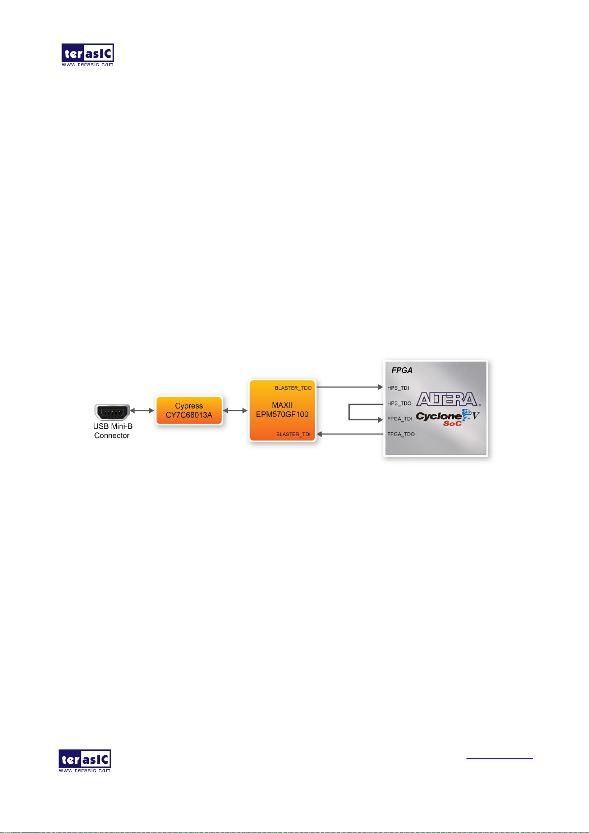
JTAG Chain on ADC-SoC Board
The FPGA device can be configured through JTAG interface on ADC-SoC board, but the JTAG
chain must form a closed loop, which allows Quartus II programmer to the detect FPGA device.
Figure 3-2 illustrates the JTAG chain on ADC-SoC board.
Figure 3-2 Path of the JTAG chain
Configure the FPGA in JTAG Mode
There are two devices (FPGA and HPS) on the JTAG chain. The following shows how the FPGA is
programmed in JTAG mode step by step.
Open the Quartus II programmer and click “Auto Detect”, as circled in Figure 3-3

ADC-SoC
User Manual
13
www.terasic.com
December 22, 2016
Figure 3-3 Detect FPGA device in JTAG mode
Select detected device associated with the board, as circled in Figure 3-4.
Figure 3-4 Select 5CSEMA4 device
Both FPGA and HPS are detected, as shown in Figure 3-5.

ADC-SoC
User Manual
14
www.terasic.com
December 22, 2016
Figure 3-5 FPGA and HPS detected in Quartus programmer
Right click on the FPGA device and open the .sof file to be programmed, as highlighted in Figure
3-6.
Figure 3-6 Open the .sof file to be programmed into the FPGA device
Select the .sof file to be programmed, as shown in Figure 3-7.

ADC-SoC
User Manual
15
www.terasic.com
December 22, 2016
Figure 3-7 Select the .sof file to be programmed into the FPGA device
Click “Program/Configure” check box and then click “Start” button to download the .sof file into
the FPGA device, as shown in Figure 3-8.
Configure the FPGA in AS Mode
Figure 3-8 Program .sof file into the FPGA device
ADC-SoC
User Manual
16
www.terasic.com
December 22, 2016
BBooaarrdd SSttaattuuss EElleemmeennttss
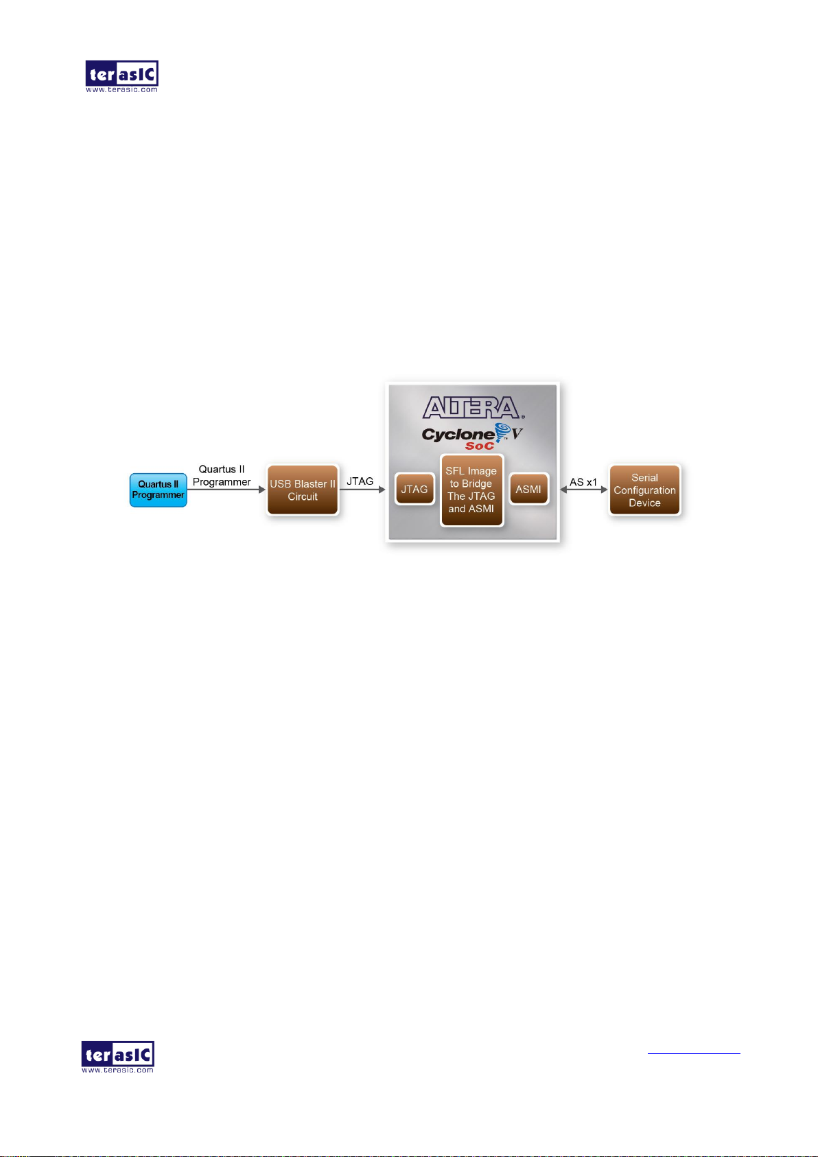
The ADC-SoC board uses a serial configuration device (EPCS128) to store configuration data for
the Cyclone V SoC FPGA. This configuration data is automatically loaded from the serial
configuration device chip into the FPGA when the board is powered up.
Users need to use Serial Flash Loader (SFL) to program the serial configuration device via JTAG
interface. The FPGA-based SFL is a soft intellectual property (IP) core within the FPGA that bridge
the JTAG and Flash interfaces. The SFL Megafunction is available in Quartus II. Figure 3-9 shows
the programming method when adopting SFL solution.
Please refer to Chapter 8: Steps of Programming the Serial Configuration Device for the basic
programming instruction on the serial configuration device.
Figure 3-9 Programming a serial configuration device with SFL solution
3.3
In addition to the 9 LEDs that FPGA/HPS device can control, there are 6 indicators which can
indicate the board status (as shown in Figure 3-10), please refer the details in Table 3-3.

ADC-SoC
User Manual
17
www.terasic.com
December 22, 2016
Board Reference
LED Name
Description
LED9
3.3-V Power
Illuminate when 3.3V power is active.
LED10
CONF_DONE
Illuminates when the FPGA is successfully configured.
LED11
JTAG_TX
Illuminate when data is transferred from JTAG to USB Host.
LED12
JTAG_RX
Illuminate when data is transferred from USB Host to JTAG.
TXD
UART TXD
Illuminate when data is transferred from FT232R to USB Host.
RXD
UART RXD
Illuminate when data is transferred from USB Host to FT232R.
BBooaarrdd RReesseett EElleemmeennttss
Figure 3-10 LED Indicators on ADC-SoC
Table 3-3 LED Indicators
3.4
There are two HPS reset buttons on ADC-SoC, HPS (cold) reset and HPS warm reset, as shown in
Figure 3-11. Table 3-4 describes the purpose of these two HPS reset buttons. Figure 3-12 is the
reset tree for ADC-SoC.

ADC-SoC
User Manual
18
www.terasic.com
December 22, 2016
Board Reference
Signal Name
Description
KEY4
HPS_RESET_N
Cold reset to the HPS, Ethernet PHY and USB host device.
Active low input which resets all HPS logics that can be reset.
KEY3
HPS_WARM_RST_N
Warm reset to the HPS block. Active low input affects the
system reset domain for debug purpose.
Figure 3-11 HPS cold reset and warm reset buttons on ADC-SoC
Table 3-4 Description of Two HPS Reset Buttons on ADC-SoC
Figure 3-12 HPS reset tree on ADC-SoC board

ADC-SoC
User Manual
19
www.terasic.com
December 22, 2016
CClloocckk CCiirrccuuiittrryy
Signal Name
FPGA Pin No.
Description
I/O Standard
FPGA_CLK1_50
PIN_V11
50 MHz clock input
3.3V
FPGA_CLK2_50
PIN_Y13
50 MHz clock input
3.3V
3.5
Figure 3-13 shows the default frequency of all external clocks to the Cyclone V SoC FPGA. A
clock generator is used to distribute clock signals with low jitter. The two 50MHz clock signals
connected to the FPGA are used as clock sources for user logic. Three 25MHz clock signal are
connected to two HPS clock inputs, and the other one is connected to the clock input of Gigabit
Ethernet Transceiver. One 24MHz clock signal is connected to the USB controller for USB Blaster
II circuit and FPGA. One 24MHz clock signals are connected to the clock inputs of USB OTG PHY.
The associated pin assignment for clock inputs to FPGA I/O pins is listed in Table 3-5.
Figure 3-13 Block diagram of the clock distribution on ADC-SoC
Table 3-5 Pin Assignment of Clock Inputs

ADC-SoC
User Manual
20
www.terasic.com
December 22, 2016
FPGA_CLK3_50
PIN_E11
50 MHz clock input (share with FPGA_CLK1_50)
3.3V
HPS_CLK1_25
PIN_E20
25 MHz clock input
3.3V
HPS_CLK2_25
PIN_D20
25 MHz clock input
3.3V
PPeerriipphheerraallss CCoonnnneecctteedd ttoo tthhee FFPPGGAA
Pushbutton releasedPushbutton depressed
Before
Debouncing
Schmitt Trigger
Debounced
3.6
This section describes the interfaces connected to the FPGA. Users can control or monitor different
interfaces with user logic from the FPGA.
3.6.1 User Push-buttons, Switches and LEDs
The board has two push-buttons connected to the FPGA, as shown in Figure 3-14. Schmitt trigger
circuit is implemented and act as switch debounce in Figure 3-15 for the push-buttons connected.
The two push-buttons named KEY0 and KEY1 coming out of the Schmitt trigger device are
connected directly to the Cyclone V SoC FPGA. The push-button generates a low logic level or
high logic level when it is pressed or not, respectively. Since the push-buttons are debounced, they
can be used as clock or reset inputs in a circuit.
Figure 3-14 Connections between the push-buttons and the Cyclone V SoC FPGA
Figure 3-15 Switch debouncing

ADC-SoC
User Manual
21
www.terasic.com
December 22, 2016
There are four slide switches connected to the FPGA, as shown in Figure 3-16. These switches are
not debounced and to be used as level-sensitive data inputs to a circuit. Each switch is connected
directly and individually to the FPGA. When the switch is set to the DOWN position (towards the
edge of the board), it generates a low logic level to the FPGA. When the switch is set to the UP
position, a high logic level is generated to the FPGA.
Figure 3-16 Connections between the slide switches and the Cyclone V SoC FPGA
There are also eight user-controllable LEDs connected to the FPGA. Each LED is driven directly
and individually by the Cyclone V SoC FPGA; driving its associated pin to a high logic level or low
level to turn the LED on or off, respectively. Figure 3-17 shows the connections between LEDs and
Cyclone V SoC FPGA. Table 3-6, Table 3-7 and Table 3-8 list the pin assignment of user
push-buttons, switches, and LEDs.
Figure 3-17 Connections between the LEDs and the Cyclone V SoC FPGA

ADC-SoC
User Manual
22
www.terasic.com
December 22, 2016
Signal Name
FPGA Pin No.
Description
I/O Standard
SW[0]
PIN_Y11
Slide Switch[0]
3.3V
SW[1]
PIN_AA11
Slide Switch[1]
3.3V
SW[2]
PIN_AD5
Slide Switch[2]
3.3V
SW[3]
PIN_AE6
Slide Switch[3]
3.3V
Signal Name
FPGA Pin No.
Description
I/O Standard
KEY[0]
PIN_AH17
Push-button[0]
3.3V
KEY[1]
PIN_AH16
Push-button[1]
3.3V
Signal Name
FPGA Pin No.
Description
I/O Standard
LED[0]
PIN_W15
LED [0]
3.3V
LED[1]
PIN_AA24
LED [1]
3.3V
LED[2]
PIN_V16
LED [2]
3.3V
LED[3]
PIN_V15
LED [3]
3.3V
LED[4]
PIN_AF26
LED [4]
3.3V
LED[5]
PIN_AE26
LED [5]
3.3V
LED[6]
PIN_Y16
LED [6]
3.3V
LED[7]
PIN_AA23
LED [7]
3.3V
Table 3-6 Pin Assignment of Slide Switches
Table 3-7 Pin Assignment of Push-buttons
Table 3-8 Pin Assignment of LEDs
ADC-SoC
User Manual
23
www.terasic.com
December 22, 2016
Supplied Voltage
Max. Current Limit
5V
1A (depend on the power adapter specification.)
3.3V
1.5A
GPIO 1 (JP7)
PIN_Y15
GPIO_1[0]
1 2
GPIO_1[1]
PIN_AC24
PIN_AA15
GPIO_1[2]
3 4
GPIO_1[3]
PIN_AD23
PIN_AG28
GPIO_1[4]
5 6
GPIO_1[5]
PIN_AF28
PIN_AE25
GPIO_1[6]
7 8
GPIO_1[7]
PIN_AF27
PIN_AG26
GPIO_1[8]
9 10
GPIO_1[9]
PIN_AH27
5V
11 12
GND PIN_AG25
GPIO_1[10]
13 14
GPIO_1[11]
PIN_AH26
PIN_AH24
GPIO_1[12]
15 16
GPIO_1[13]
PIN_AF25
PIN_AG23
GPIO_1[14]
17 18
GPIO_1[15]
PIN_AF23
PIN_AG24
GPIO_1[16]
19 20
GPIO_1[17]
PIN_AH22
PIN_AH21
GPIO_1[18]
21 22
GPIO_1[19]
PIN_AG21
PIN_AH23
GPIO_1[20]
23 24
GPIO_1[21]
PIN_AA20
PIN_AF22
GPIO_1[22]
25 26
GPIO_1[23]
PIN_AE22
PIN_AG20
GPIO_1[24]
27 28
GPIO_1[25]
PIN_AF21
3.3V
29 30
GND PIN_AG19
GPIO_1[26]
31 32
GPIO_1[27]
PIN_AH19
PIN_AG18
GPIO_1[28]
33 34
GPIO_1[29]
PIN_AH18
PIN_AF18
GPIO_1[30]
35 36
GPIO_1[31]
PIN_AF20
PIN_AG15
GPIO_1[32]
37 38
GPIO_1[33]
PIN_AE20
PIN_AE19
GPIO_1[34]
39 40
GPIO_1[35]
PIN_AE17
3.6.2 2x20 GPIO Expansion Headers
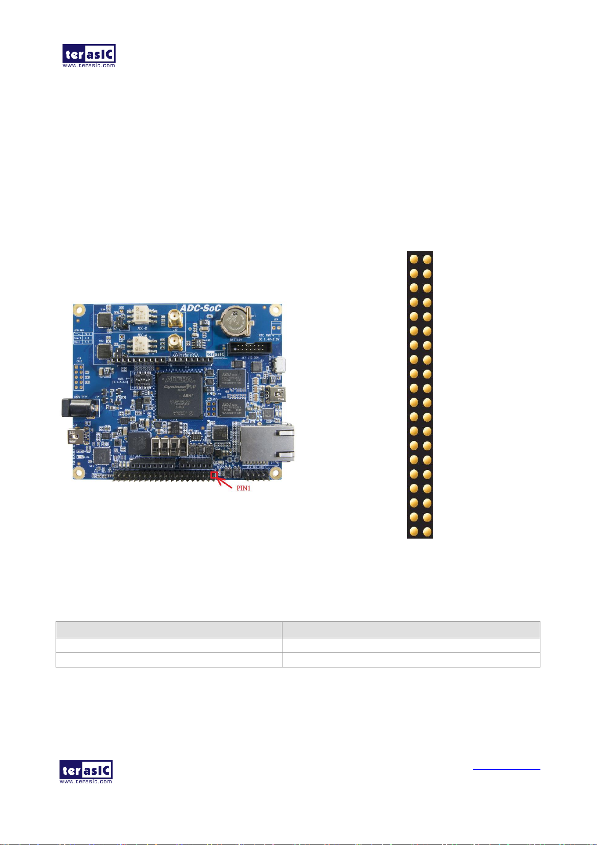
The board has one 40-pin expansion headers. Each header has 36 user pins connected directly to the
Cyclone V SoC FPGA. It also comes with DC +5V (VCC5), DC +3.3V (VCC3P3), and two GND
pins. Figure 3-18 shows the I/O distribution of the GPIO connector. The maximum power
consumption allowed for a daughter card connected to one or two GPIO ports is shown in Table 3-9
and Table 3-10 shows all the pin assignments of the GPIO connector.
Figure 3-18 GPIO Pin Arrangement
Table 3-9 Voltage and Max. Current Limit of Expansion Header(s)

ADC-SoC
User Manual
24
www.terasic.com
December 22, 2016
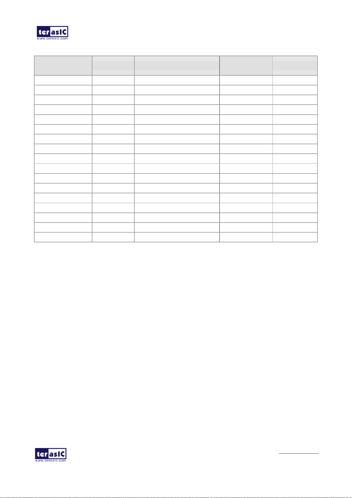
Signal Name
FPGA Pin No.
Description
I/O Standard
GPIO_1[0]
PIN_Y15
GPIO Connection 1[0]
3.3V
GPIO_1[1]
PIN_AC24
GPIO Connection 1[1]
3.3V
GPIO_1[2]
PIN_AA15
GPIO Connection 1[2]
3.3V
GPIO_1[3]
PIN_AD23
GPIO Connection 1[3]
3.3V
GPIO_1[4]
PIN_AG28
GPIO Connection 1[4]
3.3V
GPIO_1[5]
PIN_AF28
GPIO Connection 1[5]
3.3V
GPIO_1[6]
PIN_AE25
GPIO Connection 1[6]
3.3V
GPIO_1[7]
PIN_AF27
GPIO Connection 1[7]
3.3V
GPIO_1[8]
PIN_AG26
GPIO Connection 1[8]
3.3V
GPIO_1[9]
PIN_AH27
GPIO Connection 1[9]
3.3V
GPIO_1[10]
PIN_AG25
GPIO Connection 1[10]
3.3V
GPIO_1[11]
PIN_AH26
GPIO Connection 1[11]
3.3V
GPIO_1[12]
PIN_AH24
GPIO Connection 1[12]
3.3V
GPIO_1[13]
PIN_AF25
GPIO Connection 1[13]
3.3V
GPIO_1[14]
PIN_AG23
GPIO Connection 1[14]
3.3V
GPIO_1[15]
PIN_AF23
GPIO Connection 1[15]
3.3V
GPIO_1[16]
PIN_AG24
GPIO Connection 1[16]
3.3V
GPIO_1[17]
PIN_AH22
GPIO Connection 1[17]
3.3V
GPIO_1[18]
PIN_AH21
GPIO Connection 1[18]
3.3V
GPIO_1[19]
PIN_AG21
GPIO Connection 1[19]
3.3V
GPIO_1[20]
PIN_AH23
GPIO Connection 1[20]
3.3V
GPIO_1[21]
PIN_AA20
GPIO Connection 1[21]
3.3V
GPIO_1[22]
PIN_AF22
GPIO Connection 1[22]
3.3V
GPIO_1[23]
PIN_AE22
GPIO Connection 1[23]
3.3V
GPIO_1[24]
PIN_AG20
GPIO Connection 1[24]
3.3V
GPIO_1[25]
PIN_AF21
GPIO Connection 1[25]
3.3V
GPIO_1[26]
PIN_AG19
GPIO Connection 1[26]
3.3V
GPIO_1[27]
PIN_AH19
GPIO Connection 1[27]
3.3V
GPIO_1[28]
PIN_AG18
GPIO Connection 1[28]
3.3V
GPIO_1[29]
PIN_AH18
GPIO Connection 1[29]
3.3V
GPIO_1[30]
PIN_AF18
GPIO Connection 1[30]
3.3V
GPIO_1[31]
PIN_AF20
GPIO Connection 1[31]
3.3V
GPIO_1[32]
PIN_AG15
GPIO Connection 1[32]
3.3V
GPIO_1[33]
PIN_AE20
GPIO Connection 1[33]
3.3V
GPIO_1[34]
PIN_AE19
GPIO Connection 1[34]
3.3V
GPIO_1[35]
PIN_AE17
GPIO Connection 1[35]
3.3V
Table 3-10 Show all Pin Assignment of Expansion Headers
3.6.3 Arduino Uno R3 Expansion Header
The board provides Arduino Uno revision 3 compatibility expansion header which comes with four

ADC-SoC
User Manual
25
www.terasic.com
December 22, 2016
independent headers. The expansion header has 17 user pins (16pins GPIO and 1pin Reset)
connected directly to the Cyclone V SoC FPGA. 6-pins Analog input connects to ADC, and also
provides DC +9V (VCC9), DC +5V (VCC5), DC +3.3V (VCC3P3 and IOREF), and three GND
pins.
Please refer to Figure 3-19 for detailed pin-out information. The blue font represents the Arduino
Uno R3 board pin-out definition.
The 16 GPIO pins are provided to the Arduino Header for digital I/O. Table 3-11 lists the all the pin
assignments of the Arduino Uno connector (digital), signal names relative to the Cyclone V SoC
FPGA.
Figure 3-19 lists the all the pin-out signal name of the Arduino Uno connector.
The blue font represents the Arduino pin-out definition.
ADC-SoC
User Manual
26
www.terasic.com
December 22, 2016
Schematic
Signal Name
FPGA Pin No.
Description
Specific features
For Arduino
I/O Standard
Arduino_IO0
PIN_AG13
Arduino IO0
RXD
3.3-V
Arduino_IO1
PIN_AF13
Arduino IO1
TXD
3.3-V
Arduino_IO2
PIN_AG10
Arduino IO2
3.3-V
Arduino_IO3
PIN_AG9
Arduino IO3
3.3-V
Arduino_IO4
PIN_U14
Arduino IO4
3.3-V
Arduino_IO5
PIN_U13
Arduino IO5
3.3-V
Arduino_IO6
PIN_AG8
Arduino IO6
3.3-V
Arduino_IO7
PIN_AH8
Arduino IO7
3.3-V
Arduino_IO8
PIN_AF17
Arduino IO8
3.3-V
Arduino_IO9
PIN_AE15
Arduino IO9
3.3-V
Arduino_IO10
PIN_AF15
Arduino IO10
SS
3.3-V
Arduino_IO11
PIN_AG16
Arduino IO11
MOSI
3.3-V
Arduino_IO12
PIN_AH11
Arduino IO12
MISO
3.3-V
Arduino_IO13
PIN_AH12
Arduino IO13
SCK
3.3-V
Arduino_IO14
PIN_AH9
Arduino IO14
SDA
3.3-V
Arduino_IO15
PIN_AG11
Arduino IO15
SCL
3.3-V
Arduino_Reset_n
PIN_AH7
Reset signal, low active.
3.3-V
Table 3-11 Pin Assignments for Arduino Uno Expansion Header connector
Besides 16 pins for digital GPIO, there are also 6 analog inputs on the Arduino Uno R3 Expansion
Header (ADC_IN0 ~ ADC_IN5). Consequently, we use ADC LTC2308 from Linear Technology on
the board for possible future analog-to-digital applications. We will introduce in the next section.
3.6.4 A/D Converter and Analog Input
The ADC-SoC has an analog-to-digital converter (LTC2308).
The LTC2308 is a low noise, 500ksps, 8-channel, 12-bit ADC with a SPI/MICROWIRE compatible
serial interface. This ADC includes an internal reference and a fully differential sample-and-hold
circuit to reduce common mode noise. The internal conversion clock allows the external serial
output data clock (SCK) to operate at any frequency up to 40MHz.
It can be configured to accept eight input signals at inputs ADC_IN0 through ADC_IN7. These
eight input signals are connected to a 2x5 header, as shown in Figure 3-20.

ADC-SoC
User Manual
27
www.terasic.com
December 22, 2016
Figure 3-20 Signals of the 2x5 Header
These Analog inputs are shared with the Arduino's analog input pin (ADC_IN0 ~ ADC_IN5),
Figure 3-21 shows the connections between the FPGA, 2x5 header, Arduino Analog input, and the
A/D converter.
More information about the A/D converter chip is available in its datasheet. It can be found on
manufacturer’s website or in the directory \Datasheet\ADC of ADC-SoC system CD.
Figure 3-21 Connections between the FPGA, 2x5 header, and the A/D converter
ADC-SoC
User Manual
28
www.terasic.com
December 22, 2016
Signal Name
FPGA Pin No.
Description
I/O Standard
ADC_SCK
PIN_V10
Serial Data Clock
3.3V
ADC_SDO
PIN_AD4
Serial Data Out (ADC to FPGA)
3.3V
ADC_SDI
PIN_AC4
Serial Data Input (FPGA to ADC)
3.3V
ADC_CONVST
PIN_U9
Conversion Start
3.3V
Table 3-12 Pin Assignment of ADC
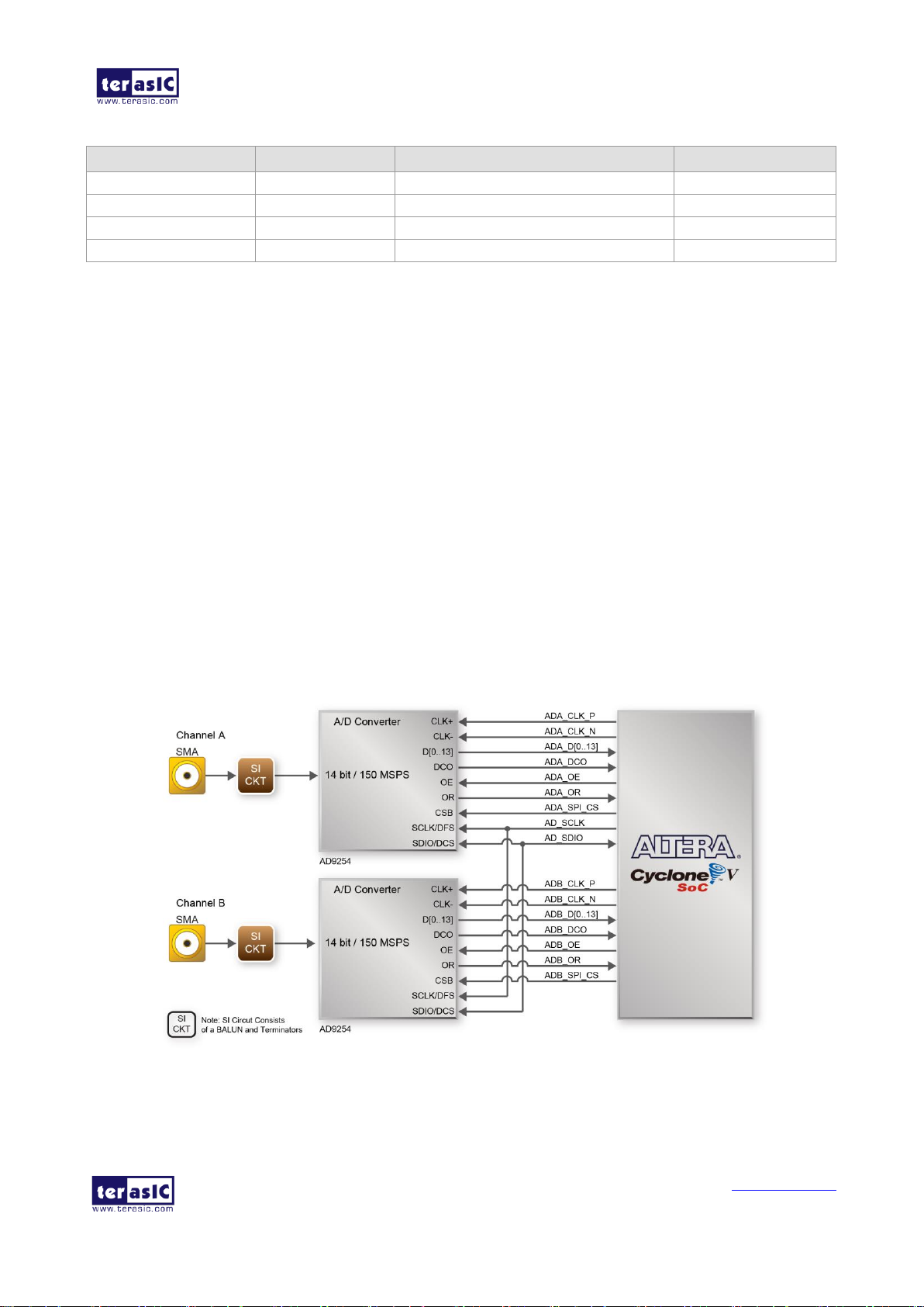
3.6.5 High-Speed A/D Converter
This board is populated with two A/D converters, which are ADI AD9254 devices, for high speed
and high-performance applications. The device uses a multistage differential pipeline architecture
with output error correction logic to provide 14-bit accuracy at 150 MSPS data rate and guarantees
no missing codes over the full operating temperature range.
The inputs to these A/D converters are transformer-coupled to create a balanced input. The
signal-to-noise ratio for the system is up to 72 dB for input signals from 1 MHz to the Nyquist
frequency of the converter. The maximum differential input voltage to the converter is 2Vpp. Usable
voltage input to the SMA connector is approximately 512 mV when it’s driven from a 50 Ohm
source.
Figure 3-22 shows the connections between the FPGA, High-Speed ADC, and SMA connector.
Table 3-13 lists the pin assignment of ADC interface connected to the FPGA.
Figure 3-22 Connections between the FPGA and High-Speed ADC.

ADC-SoC
User Manual
29
www.terasic.com
December 22, 2016
Signal Name
FPGA Pin No.
Description
I/O Standard
ADA_CLK_P
PIN_AG5
Clock Input (+)
3.3V
ADA_CLK_N
PIN_AH4
Clock Input (-)
3.3V
ADA_D0
PIN_AC22
Data Output Bit 0
3.3V
ADA_D1
PIN_AC23
Data Output Bit 1
3.3V
ADA_D2
PIN_AD17
Data Output Bit 2
3.3V
ADA_D3
PIN_AH3
Data Output Bit 3
3.3V
ADA_D4
PIN_AF7
Data Output Bit 4
3.3V
ADA_D5
PIN_AH13
Data Output Bit 5
3.3V
ADA_D6
PIN_AF4
Data Output Bit 6
3.3V
ADA_D7
PIN_AH14
Data Output Bit 7
3.3V
ADA_D8
PIN_AE9
Data Output Bit 8
3.3V
ADA_D9
PIN_AE7
Data Output Bit 9
3.3V
ADA_D10
PIN_AE8
Data Output Bit 10
3.3V
ADA_D11
PIN_AE4
Data Output Bit 11
3.3V
ADA_D12
PIN_AE23
Data Output Bit 12
3.3V
ADA_D13
PIN_AE24
Data Output Bit 13
3.3V
ADA_DCO
PIN_V12
Data Clock Output
3.3V
ADA_OE
PIN_Y17
Output Enable (Active Low)
3.3V
ADA_OR
PIN_AG14
Out-of-Range Indicator
3.3V
ADA_SPI_CS
PIN_AA19
Serial Port Interface Chip Select
(Active Low)
3.3V
ADA_PWDN
PIN_Y18
Power-Down (Not Connection )
3.3V
ADB_CLK_P
PIN_E8
Clock Input (+)
3.3V
ADB_CLK_N
PIN_D8
Clock Input (-)
3.3V
ADB_D0
PIN_AH2
Data Output Bit 0
3.3V
ADB_D1
PIN_AH5
Data Output Bit 1
3.3V
ADB_D2
PIN_AF5
Data Output Bit 2
3.3V
ADB_D3
PIN_AG6
Data Output Bit 3
3.3V
ADB_D4
PIN_AF6
Data Output Bit 4
3.3V
ADB_D5
PIN_AH6
Data Output Bit 5
3.3V
ADB_D6
PIN_AF8
Data Output Bit 6
3.3V
ADB_D7
PIN_AF9
Data Output Bit 7
3.3V
ADB_D8
PIN_AF10
Data Output Bit 8
3.3V
ADB_D9
PIN_AF11
Data Output Bit 9
3.3V
ADB_D10
PIN_AD10
Data Output Bit 10
3.3V
ADB_D11
PIN_AE11
Data Output Bit 11
3.3V
ADB_D12
PIN_AD11
Data Output Bit 12
3.3V
ADB_D13
PIN_AE12
Data Output Bit 13
3.3V
ADB_DCO
PIN_D12
Data Clock Output
3.3V
ADB_OE
PIN_T12
Output Enable (Active Low)
3.3V
ADB_OR
PIN_AD12
Out-of-Range Indicator
3.3V
ADB_SPI_CS
PIN_AD19
Serial Port Interface Chip Select
(Active Low)
3.3V
Table 3-13 Pin Assignment of High-Speed ADC AD9254 devices.

ADC-SoC
User Manual
30
www.terasic.com
December 22, 2016
ADB_PWDN
PIN_T13
Power-Down (Not Connection )
3.3V
AD_SCLK
PIN_T11
Serial Port Interface (SPI) Clock
(Serial Port Mode)
3.3V
AD_SDIO
PIN_U11
Serial Port Interface (SPI) Data
Input/output (Serial Port Mode)
3.3V
Part reference
Jumper Status
Description
Input range
J25
Open
Set VREF = 1.0 V
Differential Span to 2.0 Vpp
2.0 Vpp
Short
Set VREF = 0.5 V
Differential Span to 1.0 Vpp
1.0 Vpp
J26
Open
Set VREF = 1.0 V
Differential Span to 2.0 Vpp
2.0 Vpp
Short
Set VREF = 0.5 V
Differential Span to 1.0 Vpp
1.0 Vpp
J21 (Channel A) and J23 (Channel B) are standard through-hole SMA connectors used to interface
the AD9254 A/D converter input with SMA cables, as shown in Figure 3-23. Users can connect the
input signal through the SMA connector via a 50 ohm coaxial cable.
J25 (Channel A) and J26 (Channel B) are 2-pin jumpers for the selection of input range, as shown in
Figure 3-23. The input range is adjustable by varying the reference voltage applied to the AD9254,
using either the internal reference or an externally applied reference voltage. The input span of the
ADC tracks reference voltage changes linearly.
When the jumper is open, the SENSE pin is connected to ground through a 1K resistor and the
reference amplifier switch is connected to the internal resistor divider. This would set the VREF to
1.0V and Differential Span to 2.0Vpp.
When the jumper is shorted, the SENSE pin is connected to the VREF and this would switch the
reference amplifier input to the SENSE pin. The completed loop will provide a 0.5V reference
output and set the Differential Span to 1.0Vpp.
Table 3-14 lists the details of each combination for the jumper settings.
The datasheet of ADI AD9254 contains more information about the A/D converter chip. It is
available from the manufacturer’s website or in the directory \Datasheet\ADC of ADC-SoC system
CD.
Table 3-14 Jumper settings for the selection of input range

ADC-SoC
User Manual
31
www.terasic.com
December 22, 2016
PPeerriipphheerraallss CCoonnnneecctteedd ttoo HHaarrdd PPrroocceessssoorr SSyysstteemm ((HHPPSS))
33..77..1
1
UUsseerr PPuusshh--bbuuttttoonnss aanndd LLEEDDss
Signal Name
FPGA Pin No.
HPS GPIO
Register/bit
Function
HPS_KEY
PIN_J18
GPIO54
GPIO1[25]
I/O
Figure 3-23 SMA connectors and jumper locations on the board.
3.7
This section introduces the interfaces connected to the HPS section of the Cyclone V SoC FPGA.
Users can access these interfaces via the HPS processor.
Similar to the FPGA, the HPS also has its set of switches, buttons, LEDs, and other interfaces
connected exclusively. Users can control these interfaces to monitor the status of HPS.
Table 3-15 gives the pin assignment of all the LEDs, switches, and push-buttons.
Table 3-15 Pin Assignment of LEDs, Switches and Push-buttons

ADC-SoC
User Manual
32
www.terasic.com
December 22, 2016
HPS_LED
PIN_A20
GPIO53
GPIO1[24]
I/O
33..77..2
2
GGiiggaabbiitt EEtthheerrnneett
Signal Name
FPGA Pin No.
Description
I/O Standard
HPS_ENET_TX_EN
PIN_A12
GMII and MII transmit enable
3.3V
HPS_ENET_TX_DATA[0]
PIN_A16
MII transmit data[0]
3.3V
HPS_ENET_TX_DATA[1]
PIN_J14
MII transmit data[1]
3.3V
HPS_ENET_TX_DATA[2]
PIN_A15
MII transmit data[2]
3.3V
HPS_ENET_TX_DATA[3]
PIN_D17
MII transmit data[3]
3.3V
HPS_ENET_RX_DV
PIN_J13
GMII and MII receive data valid
3.3V
The board supports Gigabit Ethernet transfer by an external Micrel KSZ9031RN PHY chip and
HPS Ethernet MAC function. The KSZ9031RN chip with integrated 10/100/1000 Mbps Gigabit
Ethernet transceiver also supports RGMII MAC interface. Figure 3-24 shows the connections
between the HPS, Gigabit Ethernet PHY, and RJ-45 connector.
The pin assignment associated to Gigabit Ethernet interface is listed in Table 3-16. More
information about the KSZ9031RN PHY chip and its datasheet, as well as the application notes,
which are available on the manufacturer’s website.
Figure 3-24 Connections between the HPS and Gigabit Ethernet
Table 3-16 Pin Assignment of Gigabit Ethernet PHY

ADC-SoC
User Manual
33
www.terasic.com
December 22, 2016
HPS_ENET_RX_DATA[0]
PIN_A14
GMII and MII receive data[0]
3.3V
HPS_ENET_RX_DATA[1]
PIN_A11
GMII and MII receive data[1]
3.3V
HPS_ENET_RX_DATA[2]
PIN_C15
GMII and MII receive data[2]
3.3V
HPS_ENET_RX_DATA[3]
PIN_A9
GMII and MII receive data[3]
3.3V
HPS_ENET_RX_CLK
PIN_J12
GMII and MII receive clock
3.3V
HPS_ENET_RESET_N
PIN_B14
Hardware Reset Signal
3.3V
HPS_ENET_MDIO
PIN_E16
Management Data
3.3V
HPS_ENET_MDC
PIN_A13
Management Data Clock Reference
3.3V
HPS_ENET_INT_N
PIN_B14
Interrupt Open Drain Output
3.3V
HPS_ENET_GTX_CLK
PIN_J15
GMII Transmit Clock
3.3V
LED (State)
LED (Definition)
Link /Activity
LEDG
LEDY
LEDG
LEDY
H H OFF
OFF
Link off
L H ON
OFF
1000 Link / No Activity
Toggle
H
Blinking
OFF
1000 Link / Activity (RX, TX)
H L OFF
ON
100 Link / No Activity
H
Toggle
OFF
Blinking
100 Link / Activity (RX, TX)
L L ON
ON
10 Link/ No Activity
Toggle
Toggle
Blinking
Blinking
10 Link / Activity (RX, TX)
33..77..3
3
UUAARRTT
There are two LEDs, green LED (LEDG) and yellow LED (LEDY), which represent the status of
Ethernet PHY (KSZ9031RN). The LED control signals are connected to the LEDs on the RJ45
connector. The state and definition of LEDG and LEDY are listed in Table 3-17. For instance, the
connection from board to Gigabit Ethernet is established once the LEDG lights on.
Table 3-17 State and Definition of LED Mode Pins
The board has one UART interface connected for communication with the HPS. This interface
doesn’t support HW flow control signals. The physical interface is implemented by UART-USB
onboard bridge from a FT232R chip to the host with an USB Mini-B connector. More information
about the chip is available on the manufacturer’s website, or in the directory
\Datasheets\UART_TO_USB of ADC-SoC system CD. Figure 3-25 shows the connections between
the HPS, FT232R chip, and the USB Mini-B connector. Table 3-18 lists the pin assignment of
UART interface connected to the HPS.

ADC-SoC
User Manual
34
www.terasic.com
December 22, 2016
Signal Name
FPGA Pin No.
Description
I/O Standard
HPS_UART_RX
PIN_A22
HPS UART Receiver
3.3V
HPS_UART_TX
PIN_B21
HPS UART Transmitter
3.3V
HPS_CONV_USB_N
PIN_C6
Reserve
3.3V
33..77..4
4
DDDDRR33 MMeemmoorryy
Signal Name
FPGA Pin No.
Description
I/O Standard
HPS_DDR3_A[0]
PIN_C28
HPS DDR3 Address[0]
SSTL-15 Class I
HPS_DDR3_A[1]
PIN_B28
HPS DDR3 Address[1]
SSTL-15 Class I
HPS_DDR3_A[2]
PIN_E26
HPS DDR3 Address[2]
SSTL-15 Class I
HPS_DDR3_A[3]
PIN_D26
HPS DDR3 Address[3]
SSTL-15 Class I
HPS_DDR3_A[4]
PIN_J21
HPS DDR3 Address[4]
SSTL-15 Class I
HPS_DDR3_A[5]
PIN_J20
HPS DDR3 Address[5]
SSTL-15 Class I
Figure 3-25 Connections between the HPS and FT232R Chip
Table 3-18 Pin Assignment of UART Interface
The DDR3 devices connected to the HPS are the exact same model as the ones connected to the
FPGA. The capacity is 1GB and the data bandwidth is in 32-bit, comprised of two x16 devices with
a single address/command bus. The signals are connected to the dedicated Hard Memory Controller
for HPS I/O banks and the target speed is 400 MHz. Table 3-19 lists the pin assignment of DDR3
and its description with I/O standard.
Table 3-19 Pin Assignment of DDR3 Memory

ADC-SoC
User Manual
35
www.terasic.com
December 22, 2016
HPS_DDR3_A[6]
PIN_C26
HPS DDR3 Address[6]
SSTL-15 Class I
HPS_DDR3_A[7]
PIN_B26
HPS DDR3 Address[7]
SSTL-15 Class I
HPS_DDR3_A[8]
PIN_F26
HPS DDR3 Address[8]
SSTL-15 Class I
HPS_DDR3_A[9]
PIN_F25
HPS DDR3 Address[9]
SSTL-15 Class I
HPS_DDR3_A[10]
PIN_A24
HPS DDR3 Address[10]
SSTL-15 Class I
HPS_DDR3_A[11]
PIN_B24
HPS DDR3 Address[11]
SSTL-15 Class I
HPS_DDR3_A[12]
PIN_D24
HPS DDR3 Address[12]
SSTL-15 Class I
HPS_DDR3_A[13]
PIN_C24
HPS DDR3 Address[13]
SSTL-15 Class I
HPS_DDR3_A[14]
PIN_G23
HPS DDR3 Address[14]
SSTL-15 Class I
HPS_DDR3_BA[0]
PIN_A27
HPS DDR3 Bank Address[0]
SSTL-15 Class I
HPS_DDR3_BA[1]
PIN_H25
HPS DDR3 Bank Address[1]
SSTL-15 Class I
HPS_DDR3_BA[2]
PIN_G25
HPS DDR3 Bank Address[2]
SSTL-15 Class I
HPS_DDR3_CAS_n
PIN_A26
DDR3 Column Address Strobe
SSTL-15 Class I
HPS_DDR3_CKE
PIN_L28
HPS DDR3 Clock Enable
SSTL-15 Class I
HPS_DDR3_CK_n
PIN_N20
HPS DDR3 Clock
Differential 1.5-V SSTL Class I
HPS_DDR3_CK_p
PIN_N21
HPS DDR3 Clock p
Differential 1.5-V SSTL Class I
HPS_DDR3_CS_n
PIN_L21
HPS DDR3 Chip Select
SSTL-15 Class I
HPS_DDR3_DM[0]
PIN_G28
HPS DDR3 Data Mask[0]
SSTL-15 Class I
HPS_DDR3_DM[1]
PIN_P28
HPS DDR3 Data Mask[1]
SSTL-15 Class I
HPS_DDR3_DM[2]
PIN_W28
HPS DDR3 Data Mask[2]
SSTL-15 Class I
HPS_DDR3_DM[3]
PIN_AB28
HPS DDR3 Data Mask[3]
SSTL-15 Class I
HPS_DDR3_DQ[0]
PIN_J25
HPS DDR3 Data[0]
SSTL-15 Class I
HPS_DDR3_DQ[1]
PIN_J24
HPS DDR3 Data[1]
SSTL-15 Class I
HPS_DDR3_DQ[2]
PIN_E28
HPS DDR3 Data[2]
SSTL-15 Class I
HPS_DDR3_DQ[3]
PIN_D27
HPS DDR3 Data[3]
SSTL-15 Class I
HPS_DDR3_DQ[4]
PIN_J26
HPS DDR3 Data[4]
SSTL-15 Class I
HPS_DDR3_DQ[5]
PIN_K26
HPS DDR3 Data[5]
SSTL-15 Class I
HPS_DDR3_DQ[6]
PIN_G27
HPS DDR3 Data[6]
SSTL-15 Class I
HPS_DDR3_DQ[7]
PIN_F28
HPS DDR3 Data[7]
SSTL-15 Class I
HPS_DDR3_DQ[8]
PIN_K25
HPS DDR3 Data[8]
SSTL-15 Class I
HPS_DDR3_DQ[9]
PIN_L25
HPS DDR3 Data[9]
SSTL-15 Class I
HPS_DDR3_DQ[10]
PIN_J27
HPS DDR3 Data[10]
SSTL-15 Class I
HPS_DDR3_DQ[11]
PIN_J28
HPS DDR3 Data[11]
SSTL-15 Class I
HPS_DDR3_DQ[12]
PIN_M27
HPS DDR3 Data[12]
SSTL-15 Class I
HPS_DDR3_DQ[13]
PIN_M26
HPS DDR3 Data[13]
SSTL-15 Class I
HPS_DDR3_DQ[14]
PIN_M28
HPS DDR3 Data[14]
SSTL-15 Class I
HPS_DDR3_DQ[15]
PIN_N28
HPS DDR3 Data[15]
SSTL-15 Class I
HPS_DDR3_DQ[16]
PIN_N24
HPS DDR3 Data[16]
SSTL-15 Class I
HPS_DDR3_DQ[17]
PIN_N25
HPS DDR3 Data[17]
SSTL-15 Class I
HPS_DDR3_DQ[18]
PIN_T28
HPS DDR3 Data[18]
SSTL-15 Class I
HPS_DDR3_DQ[19]
PIN_U28
HPS DDR3 Data[19]
SSTL-15 Class I
HPS_DDR3_DQ[20]
PIN_N26
HPS DDR3 Data[20]
SSTL-15 Class I
HPS_DDR3_DQ[21]
PIN_N27
HPS DDR3 Data[21]
SSTL-15 Class I
HPS_DDR3_DQ[22]
PIN_R27
HPS DDR3 Data[22]
SSTL-15 Class I
HPS_DDR3_DQ[23]
PIN_V27
HPS DDR3 Data[23]
SSTL-15 Class I

ADC-SoC
User Manual
36
www.terasic.com
December 22, 2016
HPS_DDR3_DQ[24]
PIN_R26
HPS DDR3 Data[24]
SSTL-15 Class I
HPS_DDR3_DQ[25]
PIN_R25
HPS DDR3 Data[25]
SSTL-15 Class I
HPS_DDR3_DQ[26]
PIN_AA28
HPS DDR3 Data[26]
SSTL-15 Class I
HPS_DDR3_DQ[27]
PIN_W26
HPS DDR3 Data[27]
SSTL-15 Class I
HPS_DDR3_DQ[28]
PIN_R24
HPS DDR3 Data[28]
SSTL-15 Class I
HPS_DDR3_DQ[29]
PIN_T24
HPS DDR3 Data[29]
SSTL-15 Class I
HPS_DDR3_DQ[30]
PIN_Y27
HPS DDR3 Data[30]
SSTL-15 Class I
HPS_DDR3_DQ[31]
PIN_AA27
HPS DDR3 Data[31]
SSTL-15 Class I
HPS_DDR3_DQS_n[0]
PIN_R16
HPS DDR3 Data Strobe n[0]
Differential 1.5-V SSTL Class I
HPS_DDR3_DQS_n[1]
PIN_R18
HPS DDR3 Data Strobe n[1]
Differential 1.5-V SSTL Class I
HPS_DDR3_DQS_n[2]
PIN_T18
HPS DDR3 Data Strobe n[2]
Differential 1.5-V SSTL Class I
HPS_DDR3_DQS_n[3]
PIN_T20
HPS DDR3 Data Strobe n[3]
Differential 1.5-V SSTL Class I
HPS_DDR3_DQS_p[0]
PIN_R17
HPS DDR3 Data Strobe p[0]
Differential 1.5-V SSTL Class I
HPS_DDR3_DQS_p[1]
PIN_R19
HPS DDR3 Data Strobe p[1]
Differential 1.5-V SSTL Class I
HPS_DDR3_DQS_p[2]
PIN_T19
HPS DDR3 Data Strobe p[2]
Differential 1.5-V SSTL Class I
HPS_DDR3_DQS_p[3]
PIN_U19
HPS DDR3 Data Strobe p[3]
Differential 1.5-V SSTL Class I
HPS_DDR3_ODT
PIN_D28
HPS DDR3 On-die Termination
SSTL-15 Class I
HPS_DDR3_RAS_n
PIN_A25
DDR3 Row Address Strobe
SSTL-15 Class I
HPS_DDR3_RESET_n
PIN_V28
HPS DDR3 Reset
SSTL-15 Class I
HPS_DDR3_WE_n
PIN_E25
HPS DDR3 Write Enable
SSTL-15 Class I
HPS_DDR3_RZQ
PIN_D25
External reference ball for
output drive calibration
1.5 V
33..77..5
5
MMiiccrroo SSDD CCaarrdd SSoocckkeett
The board supports Micro SD card interface with x4 data lines. It serves not only an external
storage for the HPS, but also an alternative boot option for ADC-SoC board. Figure 3-26 shows
signals connected between the HPS and Micro SD card socket.
Table 3-20 lists the pin assignment of Micro SD card socket to the HPS.

ADC-SoC
User Manual
37
www.terasic.com
December 22, 2016
Signal Name
FPGA Pin No.
Description
I/O Standard
HPS_SD_CLK
PIN_B8
HPS SD Clock
3.3V
HPS_SD_CMD
PIN_D14
HPS SD Command Line
3.3V
HPS_SD_DATA[0]
PIN_C13
HPS SD Data[0]
3.3V
HPS_SD_DATA[1]
PIN_B6
HPS SD Data[1]
3.3V
HPS_SD_DATA[2]
PIN_B11
HPS SD Data[2]
3.3V
HPS_SD_DATA[3]
PIN_B9
HPS SD Data[3]
3.3V
33..77..6
6
UUSSBB 22..00 OOTTGG PPHHYY
Figure 3-26 Connections between the FPGA and SD card socket
Table 3-20 Pin Assignment of Micro SD Card Socket
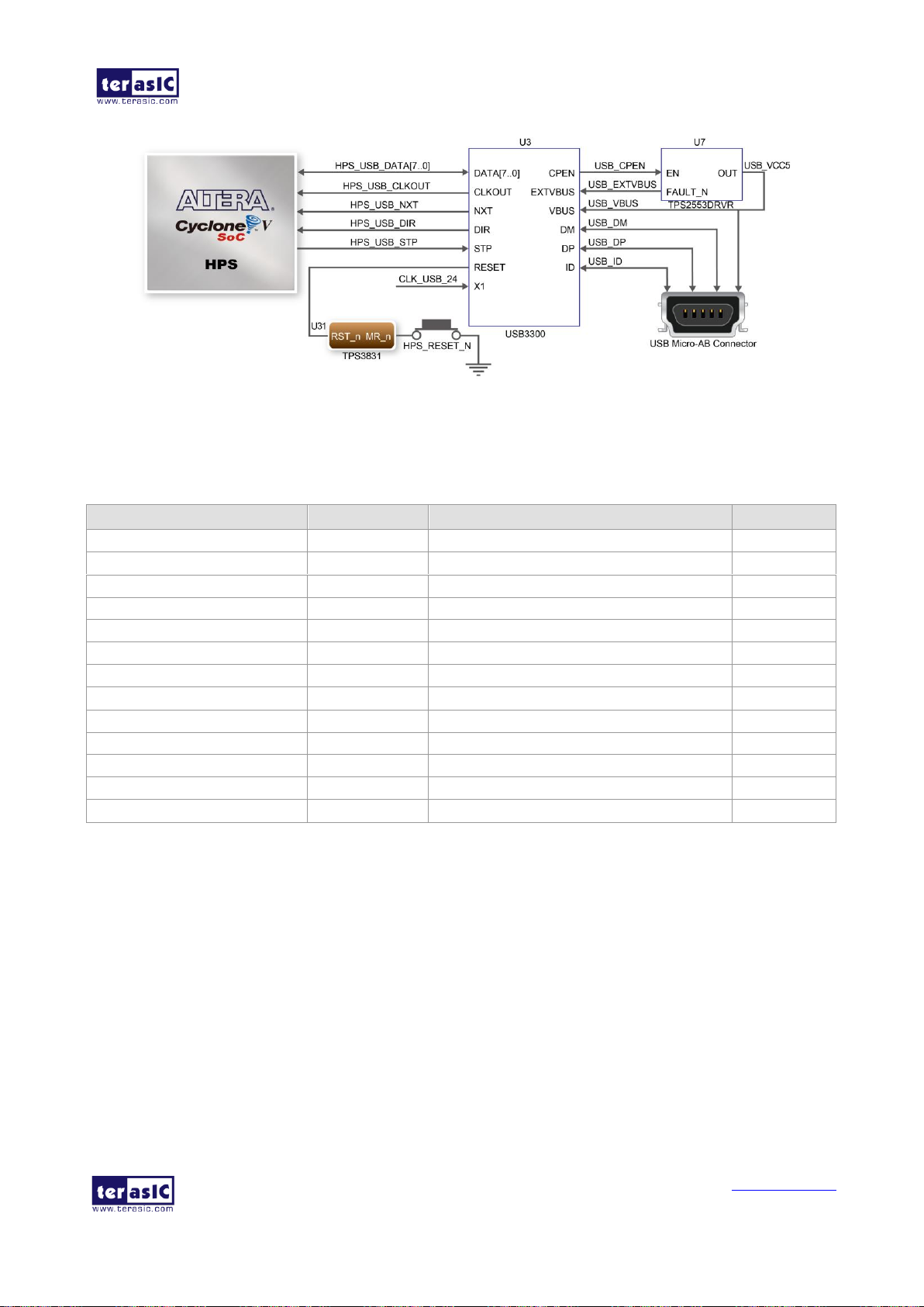
The board provides USB interfaces using the SMSC USB3300 controller. A SMSC USB3300
device in a 32-pin QFN package device is used to interface to a single Type AB Micro-USB
connector. This device supports UTMI+ Low Pin Interface (ULPI) to communicate to USB 2.0
controller in HPS. As defined by OTG mode, the PHY can operate in Host or Device modes. When
operating in Host mode, the interface will supply the power to the device through the Micro-USB
interface. Figure 3-27 shows the connections of USB PTG PHY to the HPS. Table 3-21 lists the pin
assignment of USB OTG PHY to the HPS.
ADC-SoC
User Manual
38
www.terasic.com
December 22, 2016
Signal Name
FPGA Pin No.
Description
I/O Standard
HPS_USB_CLKOUT
PIN_G4
60MHz Reference Clock Output
3.3V
HPS_USB_DATA[0]
PIN_C10
HPS USB_DATA[0]
3.3V
HPS_USB_DATA[1]
PIN_F5
HPS USB_DATA[1]
3.3V
HPS_USB_DATA[2]
PIN_C9
HPS USB_DATA[2]
3.3V
HPS_USB_DATA[3]
PIN_C4
HPS USB_DATA[3]
3.3V
HPS_USB_DATA[4]
PIN_C8
HPS USB_DATA[4]
3.3V
HPS_USB_DATA[5]
PIN_D4
HPS USB_DATA[5]
3.3V
HPS_USB_DATA[6]
PIN_C7
HPS USB_DATA[6]
3.3V
HPS_USB_DATA[7]
PIN_F4
HPS USB_DATA[7]
3.3V
HPS_USB_DIR
PIN_E5
Direction of the Data Bus
3.3V
HPS_USB_NXT
PIN_D5
Throttle the Data
3.3V
HPS_USB_RESET
PIN_H12
HPS USB PHY Reset
3.3V
HPS_USB_STP
PIN_C5
Stop Data Stream on the Bus
3.3V
33..77..7
7
GG--sseennssoorr
Figure 3-27 Connections between the HPS and USB OTG PHY
Table 3-21 Pin Assignment of USB OTG PHY
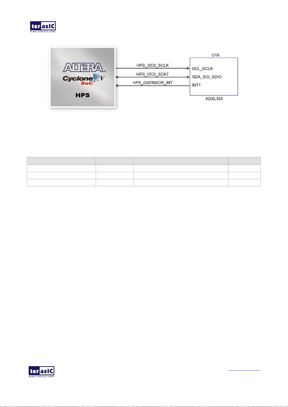
The board comes with a digital accelerometer sensor module (ADXL345), commonly known as
G-sensor. This G-sensor is a small, thin, ultralow power assumption 3-axis accelerometer with
high-resolution measurement. Digitalized output is formatted as 16-bit in two’s complement and
can be accessed through I2C interface. The I2C address of G-sensor is 0xA6/0xA7. More
information about this chip can be found in its datasheet, which is available on manufacturer’s
website or in the directory \Datasheet\G-Sensor folder of ADC-SoC system CD. Figure 3-28 shows
the connections between the HPS and G-sensor. Table 3-22 lists the pin assignment of G-senor to
the HPS.
ADC-SoC
User Manual
39
www.terasic.com
December 22, 2016
Signal Name
FPGA Pin No.
Description
I/O Standard
HPS_GSENSOR_INT
PIN_A17
HPS GSENSOR Interrupt Output
3.3V
HPS_I2C0_SCLK
PIN_C18
HPS I2C0 Clock
3.3V
HPS_I2C0_SDAT
PIN_A19
HPS I2C0 Data
3.3V
33..77..8
8
LLTTCC CCoonnnneeccttoorr
Figure 3-28 Connections between HPS and G-Sensor device.
Table 3-22 Pin Assignment of G-senor
The board has a 14-pin header, which is originally used to communicate with various daughter
cards from Linear Technology. It is connected to the SPI Master and I2C ports of HPS. The
communication with these two protocols is bi-directional. The 14-pin header can also be used for
GPIO, SPI, or I2C based communication with the HPS. Connections between the HPS and LTC
connector are shown in Figure 3-29, and the pin assignment of LTC connector is listed in Table
3-23.

ADC-SoC
User Manual
40
www.terasic.com
December 22, 2016
Signal Name
FPGA Pin No.
Description
I/O Standard
HPS_LTC_GPIO
PIN_H13
HPS LTC GPIO
3.3V
HPS_I2C1_SCLK
PIN_B21
HPS I2C1 Clock
3.3V
HPS_I2C1_SDAT
PIN_A21
HPS I2C1 Data
3.3V
HPS_SPIM_CLK
PIN_C19
SPI Clock
3.3V
HPS_SPIM_MISO
PIN_B19
SPI Master Input/Slave Output
3.3V
HPS_SPIM_MOSI
PIN_B16
SPI Master Output /Slave Input
3.3V
HPS_SPIM_SS
PIN_C16
SPI Slave Select
3.3V
33..77..9
9
RReeaall--TTiimmee CClloocckk
Figure 3-29 Connections between the HPS and LTC connector
Table 3-23 Pin Assignment of LTC Connector
This board is populated with a real-time clock (RTC) DS1339C, which is a low-power clock / date
device manufactured by MAXIM. The clock/date provides seconds, minutes, hours, day, date,
month, and year information. The date at the end of the month is automatically adjusted for months
less than 31 days, including correction for leap year. The clock operates in either 24-hour or 12-hour
format with AM/PM indicator.

ADC-SoC
User Manual
41
www.terasic.com
December 22, 2016
Signal Name
FPGA Pin No.
Description
I/O Standard
HPS_I2C0_SCLK
PIN_C18
HPS I2C0 Clock
3.3V
HPS_I2C0_SDAT
PIN_A19
HPS I2C0 Data
3.3V
The I2C address of RTC is 0xD0/0xD1 and its I2C bus is shared with the G-sensor (ADXL345).
The datasheet of DS1339C has more information about this chip. It is available on manufacturer’s
website or in the directory \Datasheet\RTC folder of ADC-SoC system CD. Figure 3-30 shows the
connections between the HPS and G-sensor / RTC. Table 3-24 lists the pin assignment of RTC to
the HPS.
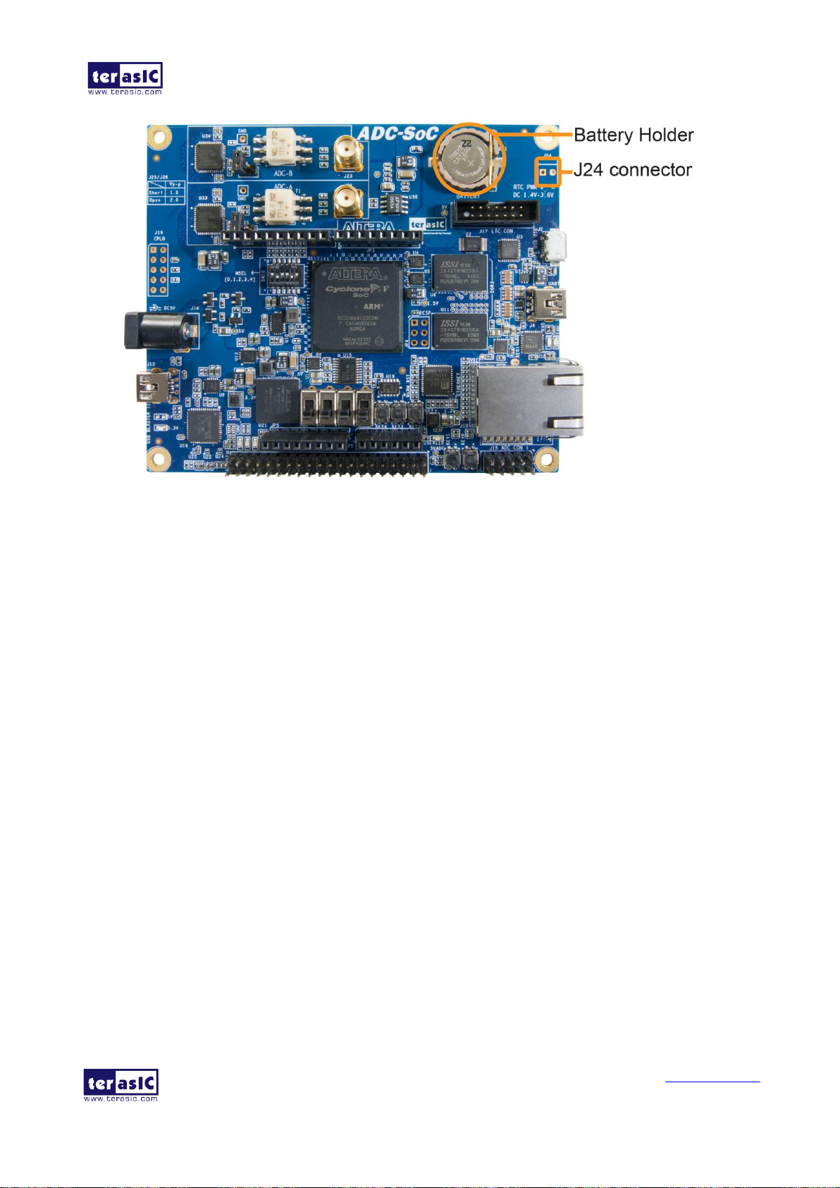
The RTC device allows the system to maintain accurate time after the main power is turned off.
This board also provides a battery holder for the unit to run after the power is turned off. Users need
to install a CR1220 button cell battery in the battery holder. Users can also solder a connector (pitch
2.54) at the J24 position using an external power supply (input voltage range 1.4V to 3.6V) for the
RTC to run. The battery holder and J24 connector are located at the top right of the board, as shown
in Figure 3-31.
Table 3-24 Pin Assignment of RTC
Figure 3-30 Connections between HPS and G-Sensor / RTC device.
ADC-SoC
User Manual
42
www.terasic.com
December 22, 2016
Figure 3-31 battery holder and J24 connector location.

ADC-SoC
User Manual
43
www.terasic.com
December 22, 2016
AADDCC--SSooCC FFaaccttoorryy CCoonnffiigguurraattiioonn
Chapter 4
Examples For FPGA
This chapter provides examples of advanced designs implemented by RTL or Qsys on the
ADC-SoC board. These reference designs cover the features of peripherals connected to the FPGA,
such as A/D Converter. All the associated files can be found in the directory \Demonstrations\FPGA
of ADC-SoC System CD.
Installation of Demonstrations
Install the demonstrations on your computer:
Copy the folder Demonstrations to a local directory of your choice. It is important to make sure the
path to your local directory contains NO space. Otherwise it will lead to error in Nios II.
Note Quartus II v16.1 or later is required for all ADC-SoC demonstrations to support Cyclone V
SoC device.
4.1
The ADC-SoC board has a default configuration bit-stream pre-programmed, which demonstrates
some of the basic features on board. The setup required for this demonstration and the location of its
files are shown below.
Demonstration Setup, File Locations, and Instructions
Project directory: ADC_SOC_Default
Bitstream used: ADC_SOC_Default.sof or ADC_SOC_Default.jic
Power on the ADC-SoC board with the USB cable connected to the USB-Blaster II port. If
necessary (that is, if the default factory configuration is not currently stored in the EPCS
device), download the bit stream to the board via JTAG interface.
You should now be able to observe the LEDs are blinking.
For the ease of execution, a demo_batch folder is provided in the project. It is able to not only

ADC-SoC
User Manual
44
www.terasic.com
December 22, 2016
LLTTCC22330088 AADDCC RReeaaddiinngg
load the bit stream into the FPGA in command line, but also program or erase .jic file to the
EPCS by executing the test.bat file shown in Figure 4-1
If users want to program a new design into the EPCS device, the easiest method is to copy the
new .sof file into the demo_batch folder and execute the test.bat. Option “2” will convert
the .sof to .jic and option”3” will program .jic file into the EPCS device.
Figure 4-1 Command line of the batch file to program the FPGA and EPCS device
4.2
This demonstration illustrates steps to evaluate the performance of the 8-channel 12-bit A/D
Converter LTC2308. The DC 5.0V on the 2x5 header is used to drive the analog signals by a
trimmer potentiometer. The voltage can be adjusted within the range between 0 and 4.096V. The
12-bit voltage measurement is displayed on the NIOS II console. Figure 4-2 shows the block
diagram of this demonstration.
If the input voltage is -2.0V ~ 2.0V, a pre-scale circuit can be used to adjust it to 0 ~ 4V.

ADC-SoC
User Manual
45
www.terasic.com
December 22, 2016
Figure 4-2 Block diagram of ADC reading
Figure 4-3 depicts the pin arrangement of the 2x5 header. This header is the input source of ADC
convertor in this demonstration. Users can connect a trimmer to the specified ADC channel
(ADC_IN0 ~ ADC_IN7) that provides voltage to the ADC convert. The FPGA will read the
associated register in the convertor via serial interface and translates it to voltage value to be
displayed on the Nios II console.
Figure 4-3 Pin distribution of the 2x5 Header for the ADC

ADC-SoC
User Manual
46
www.terasic.com
December 22, 2016
System Requirements
The following items are required for this demonstration.
ADC-SoC board x1
Trimmer Potentiometer x1
Wire Strip x3
Demonstration File Locations
Hardware project directory: ADC_SOC_ADC
Bitstream used: ADCSOC_ADC.sof
Software project directory: ADC_SOC_ADC \software
Demo batch file : ADC_SOC_ADC \demo_batch\ test.bat
Demonstration Setup and Instructions
Connect the trimmer to corresponding ADC channel on the 2x5 header, as shown in Figure 4-4,
as well as the +5V and GND signals. The setup shown above is connected to ADC channel 0.
Execute the demo batch file test.bat to load the bitstream and software execution file to the
FPGA.
The Nios II console will display the voltage of the specified channel voltage result information
Figure 4-4 Hardware setup for the ADC reading demonstration

ADC-SoC
User Manual
47
www.terasic.com
December 22, 2016
HHIIGGHH SSPPEEEEDD AADDCC AADD99225544
4.3
This demo takes the waveform of an external signal generator as the input of ADC-SoC via ADC-A
and/or ADC-B through SMA_A and/or SMA_B connector, respectively. Users can observe the
original incoming waveform and the rectified waveform by the FPGA simultaneously. Figure 4-5
shows the block diagram of this demonstration.
Figure 4-5 Block diagram of HIGH-SPEED-ADC
The function of each block is listed below:
PLL: This block takes the 50MHz clock on ADC-SoC and generates the SYS_CLK (150MHz) for
the two ADC IC and FPGA.
ADC-A/B: These blocks represent the two AD9254 IC on ADC-SoC. Each one is 14-bit high-speed
parallel Analog-to-Digital converter. .
TWO_CH_ADC_SYNC: This block synchronizes the data of AD9254 with SYS_CLK.
ADC_RD_DET: This block has two functions performed by the two submodules. (1) the module
WAVE_RECT takes the absolute value of incoming waveform. (2) the module SIGNAL_DET
serves as the detector of incoming signal, which generates 1 or 0, depending on the absolute value
of incoming signal is greater or less than the threshold, respectively.
USB_Blaster : This block establishes connection to the host PC and it can be used to observe the
waveform of incoming signal in real time and the rectified waveform in SignalTap II in Quartus
software.

ADC-SoC
User Manual
48
www.terasic.com
December 22, 2016
System Requirements
The following items are required for this demonstration.
ADC-SoC Board x1
Signal Generator x1
SMA Cable x1
Demonstration File Locations
Hardware project directory: ADC_SoC_HIGH_SPEED_ADC
Bitstream used: ADC_SoC_HIGH_SPEED_ADC.sof
Demo batch file : ADC_SoC_HIGH_SPEED_ADC\demo_batch\ test.bat
SignalTapeII file : ADC_SoC_HIGH_SPEED_ADC\demo_batch\ViewWave.stp
Demonstration Setup and Instructions
Connect the output of a signal generator to the SMA connector J21 (ADC-A) or J23 (ADC-B)
of ADC-SoC, as shown in Figure 4-6.
Figure 4-6 Hardware setup for the HIGH-SPEED-ADC
Connect the 5V adapter to the J14 of ADC-SoC. Connect the J13 of ADC-SoC to the host PC
Execute the demo batch file test.bat to load the bitstream file to the FPGA.
Open ViewWave.stp and click RUN to observe the waveform change of incoming signal in real
via mini USB cable.

ADC-SoC
User Manual
49
www.terasic.com
December 22, 2016
time, as shown in Figure 4-7. The LED0 and LED1 correspond to ADC-A and ADC-B,
respectively. They will lit when the incoming signal exceeds the threshold.
Signal comes in from Channel A
Signal comes in from Channel B
Figure 4-7 SignalTape II viewer for the HIGH-SPEED-ADC
(1) SADA_D and SADB_D correspond to the 14-bit incoming parallel data from the two
AD9254 IC.
(2) PD_A and PD_B represent the absolute values of the two ADC.
(3) HAVE_A and HAVE_B are either 1 or 0, depending on the absolute value of ADC is greater
or less than the threshold, respectively.

ADC-SoC
User Manual
50
www.terasic.com
December 22, 2016
UUsseerrss LLEEDD aanndd KKEEYY
Chapter 5
Examples for
HPS SoC
This chapter provides several C-code examples based on the Terasic Linux BPS. These examples
demonstrate major features of peripherals connected to HPS interface on ADC-SoC board such as
users LED/KEY, I2C interfaced G-sensor. All the associated files can be found in the directory
Demonstrations/SOC of the ADC-SoC System CD.
Installation of the Demonstrations
To install the demonstrations on the host computer:
Copy the directory Demonstrations into a local directory of your choice. SoC EDS v16.1 is
required for users to compile the c-code project.
5.1
This demonstration shows how to control the users LED and KEY by accessing the register of
GPIO controller through the memory-mapped device driver. The memory-mapped device driver
allows developer to access the system physical memory.
Function Block Diagram
Figure 5-1 shows the function block diagram of this demonstration. The users LED and KEY are
connected to the GPIO1 controller in HPS. The behavior of GPIO controller is controlled by the
register in GPIO controller. The registers can be accessed by application software through the
memory-mapped device driver, which is built into SoC Linux.

ADC-SoC
User Manual
51
www.terasic.com
December 22, 2016
Figure 5-1 Block diagram of GPIO demonstration
Block Diagram of GPIO Interface
The HPS provides three general-purpose I/O (GPIO) interface modules. Figure 5-2 shows the block
diagram of GPIO Interface. GPIO[28..0] is controlled by the GPIO0 controller and GPIO[57..29] is
controlled by the GPIO1 controller. GPIO[70..58] and input-only GPI[13..0] are controlled by the
GPIO2 controller.
GPIO Register Block
The behavior of I/O pin is controlled by the registers in the register block. There are three 32-bit
Figure 5-2 Block diagram of GPIO Interface

ADC-SoC
User Manual
52
www.terasic.com
December 22, 2016
registers in the GPIO controller used in this demonstration. The registers are:
gpio_swporta_dr: write output data to output I/O pin
gpio_swporta_ddr: configure the direction of I/O pin
gpio_ext_porta: read input data of I/O input pin
The gpio_swporta_ddr configures the LED pin as output pin and drives it high or low by writing
data to the gpio_swporta_dr register. The first bit (least significant bit) of gpio_swporta_dr
controls the direction of first IO pin in the associated GPIO controller and the second bit controls
the direction of second IO pin in the associated GPIO controller and so on. The value "1" in the
register bit indicates the I/O direction is output, while the value "0" in the register bit indicates the
I/O direction is input.
The first bit of gpio_swporta_dr register controls the output value of first I/O pin in the associated
GPIO controller, the second bit controls the output value of second I/O pin in the associated GPIO
controller and so on. The value "1" in the register bit indicates the output value is high, and the
value "0" indicates the output value is low.
The status of KEY can be queried by reading the value of gpio_ext_porta register. The first bit
represents the input status of first IO pin in the associated GPIO controller, and the second bit
represents the input status of second IO pin in the associated GPIO controller and so on. The value
"1" in the register bit indicates the input state is high, and the value "0" indicates the input state is
low.
GPIO Register Address Mapping
The registers of HPS peripherals are mapped to HPS base address space 0xFC000000 with 64KB
size. The registers of the GPIO1 controller are mapped to the base address 0xFF708000 with 4KB
size, and the registers of the GPIO2 controller are mapped to the base address 0xFF70A000 with
4KB size, as shown in Figure 5-3.

ADC-SoC
User Manual
53
www.terasic.com
December 22, 2016
#include <stdio.h>
#include <unistd.h>
#include <fcntl.h>
#include <sys/mman.h>
Figure 5-3 GPIO address map
Software API
Developers can use the following software API to access the register of GPIO controller.
open: open memory mapped device driver
mmap: map physical memory to user space
alt_read_word: read a value from a specified register
alt_write_word: write a value into a specified register
munmap: clean up memory mapping
close: close device driver.
Developers can also use the following MACRO to access the register
alt_setbits_word: set specified bit value to one for a specified register
alt_clrbits_word: set specified bit value to zero for a specified register
The program must include the following header files to use the above API to access the registers of
GPIO controller.

ADC-SoC
User Manual
54
www.terasic.com
December 22, 2016
#include "hwlib.h"
#include "socal/socal.h"
#include "socal/hps.h"
#include "socal/alt_gpio.h"
LED and KEY Control
Figure 5-4 shows the HPS users LED and KEY pin assignment for the ADC-SoC board. The LED
is connected to HPS_GPIO53 and the KEY is connected to HPS_GPIO54. They are controlled by
the GPIO1 controller, which also controls HPS_GPIO29 ~ HPS_GPIO57.
Figure 5-4 Pin assignment of LED and KEY
Figure 5-5 shows the gpio_swporta_ddr register of the GPIO1 controller. The bit-0 controls the
pin direction of HPS_GPIO29. The bit-24 controls the pin direction of HPS_GPIO53, which
connects to HPS_LED, the bit-25 controls the pin direction of HPS_GPIO54, which connects to
HPS_KEY , and so on. The pin direction of HPS_LED and HPS_KEY are controlled by the bit-24
and bit-25 in the gpio_swporta_ddr register of the GPIO1 controller, respectively. Similarly, the
output status of HPS_LED is controlled by the bit-24 in the gpio_swporta_dr register of the
GPIO1 controller. The status of KEY can be queried by reading the value of the bit-24 in the
gpio_ext_porta register of the GPIO1 controller.
The following mask is defined in the demo code to control LED and KEY direction and LED’s
Figure 5-5 gpio_swporta_ddr register in the GPIO1 controller
ADC-SoC
User Manual
55
www.terasic.com
December 22, 2016
#define USER_IO_DIR (0x01000000)
#define BIT_LED (0x01000000)
#define BUTTON_MASK (0x02000000)
alt_setbits_word( ( virtual_base +
( ( uint32_t )( ALT_GPIO1_SWPORTA_DDR_ADDR ) &
( uint32_t )( HW_REGS_MASK ) ) ), USER_IO_DIR );
alt_setbits_word( ( virtual_base +
( ( uint32_t )( ALT_GPIO1_SWPORTA_DR_ADDR ) &
( uint32_t )( HW_REGS_MASK ) ) ), BIT_LED );
alt_read_word( ( virtual_base +
( ( uint32_t )( ALT_GPIO1_EXT_PORTA_ADDR ) &
( uint32_t )( HW_REGS_MASK ) ) ) );
output value.
The following statement is used to configure the LED associated pins as output pins.
The following statement is used to turn on the LED.
The following statement is used to read the content of gpio_ext_porta register. The bit mask is used
to check the status of the key.
Demonstration Source Code
Build tool: SoC EDS V16.1
Project directory: \Demonstration\SoC\hps_gpio
Binary file: hps_gpio
Build command: make ('make clean' to remove all temporal files)
Execute command: ./hps_gpio
Demonstration Setup
Connect a USB cable to the USB-to-UART connector (J4) on the ADC-SoC board and the host
PC.
Copy the executable file "hps_gpio" into the microSD card under the "/home/root" folder in
Linux.
Insert the booting micro SD card into the ADC-SoC board.
Power on the ADC-SoC board.

ADC-SoC
User Manual
56
www.terasic.com
December 22, 2016
II22CC IInntteerrffaacceedd GG--sseennssoorr
Launch PuTTY and establish connection to the UART port of Putty. Type "root" to login
Linux.
Type "./hps_gpio " in the UART terminal of PuTTY to start the program.
HPS_LED will flash twice and users can control the user LED with push-button.
Press HPS_KEY to light up HPS_LED.
Press "CTRL + C" to terminate the application.
5.2
This demonstration shows how to control the G-sensor by accessing its registers through the built-in
I2C kernel driver in Terasic Linux BSP.
Function Block Diagram
Figure 5-6 shows the function block diagram of this demonstration. The G-sensor on the ADC-SoC
board is connected to the I2C0 controller in HPS. The G-Sensor I2C 7-bit device address is 0x53.
The system I2C bus driver is used to access the register files in the G-sensor. The G-sensor interrupt
signal is connected to the PIO controller. This demonstration uses polling method to read the
register data.
Figure 5-6 Block diagram of the G-sensor demonstration
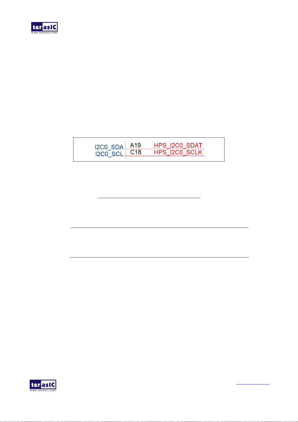
ADC-SoC
User Manual
57
www.terasic.com
December 22, 2016
I2C Driver
The procedures to read a register value from G-sensor register files by the existing I2C bus driver in
the system are:
1. Open I2C bus driver "/dev/i2c-0": file = open("/dev/i2c-0", O_RDWR);
2. Specify G-sensor's I2C address 0x53: ioctl(file, I2C_SLAVE, 0x53);
3. Specify desired register index in g-sensor: write(file, &Addr8, sizeof(unsigned char));
4. Read one-byte register value: read(file, &Data8, sizeof(unsigned char));
The G-sensor I2C bus is connected to the I2C0 controller, as shown in the Figure 5-7. The driver
name given is '/dev/i2c-0'.
Figure 5-7 Connection of HPS I2C signals
The step 4 above can be changed to the following to write a value into a register.
write(file, &Data8, sizeof(unsigned char));
The step 4 above can also be changed to the following to read multiple byte values.
read(file, &szData8, sizeof(szData8)); // where szData is an array of bytes
The step 4 above can be changed to the following to write multiple byte values.
write(file, &szData8, sizeof(szData8)); // where szData is an array of bytes
G-sensor Control
The ADI ADXL345 provides I2C and SPI interfaces. I2C interface is selected by setting the CS pin
to high on the ADC-SoC board.
The ADI ADXL345 G-sensor provides user-selectable resolution up to 13-bit ± 16g. The
resolution can be configured through the DATA_FORAMT(0x31) register. The data format in this
demonstration is configured as:
Full resolution mode
± 16g range mode
Left-justified mode

ADC-SoC
User Manual
58
www.terasic.com
December 22, 2016
The X/Y/Z data value can be derived from the DATAX0(0x32), DATAX1(0x33), DATAY0(0x34),
DATAY1(0x35), DATAZ0(0x36), and DATAX1(0x37) registers. The DATAX0 represents the least
significant byte and the DATAX1 represents the most significant byte. It is recommended to
perform multiple-byte read of all registers to prevent change in data between sequential registers
read. The following statement reads 6 bytes of X, Y, or Z value.
read(file, szData8, sizeof(szData8)); // where szData is an array of six-bytes
Demonstration Source Code
Build tool: SoC EDS v16.1
Project directory: \Demonstration\SoC\hps_gsensor
Binary file: gsensor
Build command: make ('make clean' to remove all temporal files)
Execute command: ./gsensor [loop count]
Demonstration Setup
Connect a USB cable to the USB-to-UART connector (J4) on the ADC-SoC board and the host
PC.
Copy the executable file "gsensor" into the microSD card under the "/home/root" folder in
Linux.
Insert the booting microSD card into the ADC-SoC board.
Power on the ADC-SoC board.
Launch PuTTY to establish connection to the UART port of ADC-SoC board. Type "root" to
login Yocto Linux.
Execute "./gsensor" in the UART terminal of PuTTY to start the G-sensor polling.
The demo program will show the X, Y, and Z values in the PuTTY, as shown in Figure 5-8.
Press "CTRL + C" to terminate the program.
Figure 5-8 Terminal output of the G-sensor demonstration

ADC-SoC
User Manual
59
www.terasic.com
December 22, 2016
HHPPSS CCoonnttrrooll FFPPGGAA LLEEDD
Chapter 6
Examples for using
both HPS SoC
and FGPA
Although HPS and FPGA can operate independently, they are tightly coupled via a high-bandwidth
system interconnect built from high-performance ARM AMBA® AXITM bus bridges. Both FPGA
fabric and HPS can access to each other via these interconnect bridges. This chapter provides
demonstrations on how to achieve superior performance and lower latency through these
interconnect bridges when comparing to solutions containing a separate FPGA and discrete
processor.
6.1
This demonstration shows how HPS controls the FPGA LED through Lightweight HPS-to-FPGA
Bridge. The FPGA is configured by HPS through FPGA manager in HPS.
A brief view on FPGA manager
The FPGA manager in HPS configures the FPGA fabric from HPS. It also monitors the state of
FPGA and drives or samples signals to or from the FPGA fabric. The command is provided to
configure FPGA through the FPGA manager. The FPGA configuration data is stored in the file
with .rbf extension. The MSEL[4:0] must be set to 00000 before executing the command on HPS.
Function Block Diagram
Figure 6-1 shows the block diagram of this demonstration. The HPS uses Lightweight
HPS-to-FPGA AXI Bridge to communicate with FPGA. The hardware in FPGA part is built into
Qsys. The data transferred through Lightweight HPS-to-FPGA Bridge is converted into Avalon-MM
master interface. The PIO Controller works as Avalon-MM slave in the system. They control the

ADC-SoC
User Manual
60
www.terasic.com
December 22, 2016
h2p_lw_led_addr=virtual_base+( ( unsigned long )( ALT_LWFPGASLVS_OFST
associated pins to change the state of LED . This is similar to a system using Nios II processor to
control LED.
Figure 6-1 FPGA LED are controlled by HPS
LED Control Software Design
The Lightweight HPS-to-FPGA Bridge is a peripheral of HPS. The software running on Linux
cannot access the physical address of the HPS peripheral. The physical address must be mapped to
the user space before the peripheral can be accessed. Alternatively, a customized device driver
module can be added to the kernel. The entire CSR span of HPS is mapped to access various
registers within that span. The mapping function and the macro defined below can be reused if any
other peripherals whose physical address is also in this span.
The start address of Lightweight HPS-to-FPGA Bridge after mapping can be retrieved by
ALT_LWFPGASLVS_OFST, which is defined in altera_hps hardware library. The slave IP
connected to the bridge can then be accessed through the base address and the register offset in
these IPs. For instance, the base address of the PIO slave IP in this system is 0x0001_0040, the
direction control register offset is 0x01, and the data register offset is 0x00. The following statement
is used to retrieve the base address of PIO slave IP .
ADC-SoC
User Manual
61
www.terasic.com
December 22, 2016
+ LED_PIO_BASE ) & ( unsigned long)( HW_REGS_MASK ) );
alt_write_word(h2p_lw_led_addr, Mask );
DDeemmoonnssttrraattiioonn SSeettuupp
Considering this demonstration only needs to set the direction of PIO as output, which is the default
direction of the PIO IP, the step above can be skipped. The following statement is used to set the
output state of the PIO.
The Mask in the statement decides which bit in the data register of the PIO IP is high or low. The
bits in data register decide the output state of the pins connected to the LED.
Demonstration Source Code
Build tool: SoC EDS V16.1
Project directory: \Demonstration\ SoC_FPGA\HPS_CONTROL_FPGA_LED
FPGA configuration file : HPS_CONTROL_FPGA_LED.rbf
Binary file: HPS_CONTROL_FPGA_LED
Build app command: make ('make clean' to remove all temporal files)
Execute app command:./ HPS_CONTROL_FPGA_LED
Quartus II and SoCEDS must be installed on the host PC.
The MSEL[4:0] is set to 00000.
Connect a USB cable to the USB-to-UART connector (J4) on the ADC-SoC board and the host
PC.
Copy the executable files "HPS_CONTROL_FPGA_LED" and the FPGA configuration file "
HPS_CONTROL_FPGA_LED.rbf " into the microSD card under the "/home/root" folder in
Linux.
Insert the booting microSD card into the ADC-SoC board.
Power on the ADC-SoC board.
Launch PuTTY to establish connection to the UART port of the ADC-SoC board. Type "root"
to login Linux.
Execute "dd if= HPS_CONTROL_FPGA_LED.rbf of=/dev/fpga0 bs=1M" in the UART
terminal of PuTTY to configure the FPGA through the FPGA manager. After the
configuration is successful, the message shown in Figure 6-2 will be displayed in the
terminal.

ADC-SoC
User Manual
62
www.terasic.com
December 22, 2016
Figure 6-2 Running command to configure the FPGA
Execute "./HPS_CONTROL_FPGA_LED" in the UART terminal of PuTTY to start the
program.
The message shown in Figure 6-3, will be displayed in the terminal. The LED[7:0] will be
flashing.
Figure 6-3 Running result in the terminal of PuTTY
Press "CTRL + C" to terminate the program.
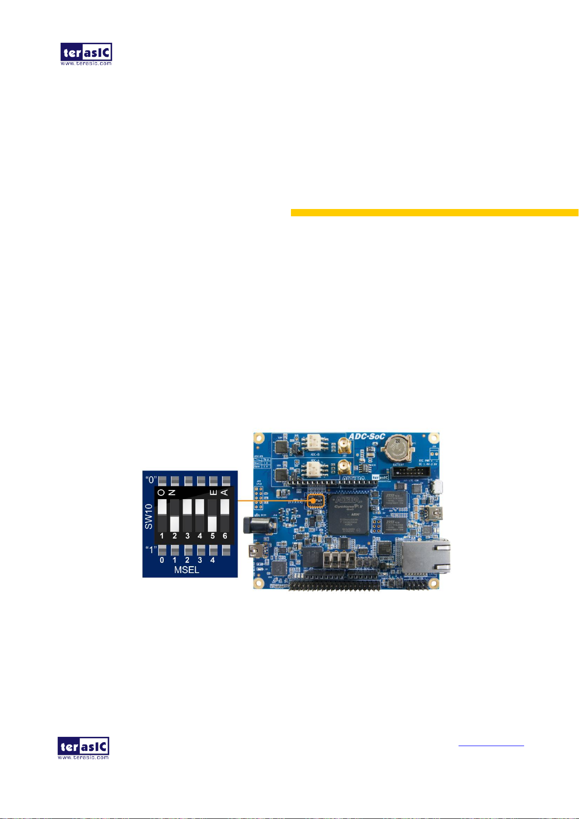
ADC-SoC
User Manual
63
www.terasic.com
December 22, 2016
BBeeffoorree PPrrooggrraammmmiinngg BBeeggiinnss
CCoonnvveerrtt ..SSOOFF FFiillee ttoo ..JJIICC FFiillee
Chapter 7
Programming the
EPCS Device
This chapter describes how to program the serial configuration (EPCS) device with Serial Flash
Loader (SFL) function via the JTAG interface. Users can program EPCS devices with a JTAG
indirect configuration (.jic) file, which is converted from a user-specified SRAM object file (.sof) in
Quartus. The .sof file is generated after the project compilation is successful. The steps of
converting .sof to .jic in Quartus II are listed below.
7.1
The FPGA should be set to AS x1 mode i.e. MSEL[4..0] = “10010” to use the Flash as a FPGA
configuration device, as shown in Figure 7-1.
Figure 7-1 DIP switch (SW10) setting of Active Serial (AS) mode
7.2
1. Choose Convert Programming Files from the File menu of Quartus II, as shown in Figure
7-2.

ADC-SoC
User Manual
64
www.terasic.com
December 22, 2016
Figure 7-2 File menu of Quartus II
2. Select JTAG Indirect Configuration File (.jic) from the Programming file type field in
the dialog of Convert Programming Files.
3. Choose EPCS128 from the Configuration device field.
4. Choose Active Serial from the Mode filed.
5. Browse to the target directory from the File name field and specify the name of output file.
6. Click on the SOF data in the section of Input files to convert, as shown in Figure 7-3.

ADC-SoC
User Manual
65
www.terasic.com
December 22, 2016
Figure 7-3 Dialog of “Convert Programming Files”
7. Click Add File.
8. Select the .sof to be converted to a .jic file from the Open File dialog.
9. Click Open.
10. Click on the Flash Loader and click Add Device, as shown in Figure 7-4.
11. Click OK and the Select Devices page will appear.

ADC-SoC
User Manual
66
www.terasic.com
December 22, 2016
Figure 7-4 Click on the “Flash Loader”
12. Select the targeted FPGA to be programed into the EPCS, as shown in Figure 7-5.
13. Click OK and the Convert Programming Files page will appear, as shown in Figure 7-6.
14. Click Generate.

ADC-SoC
User Manual
67
www.terasic.com
December 22, 2016
Figure 7-5 “Select Devices” page
Figure 7-6 “Convert Programming Files” page after selecting the device

ADC-SoC
User Manual
68
www.terasic.com
December 22, 2016
WWrriittee JJIICC FFiillee iinnttoo tthhee EEPPCCSS DDeevviiccee
7.3
When the conversion of SOF-to-JIC file is complete, please follow the steps below to program the
EPCS device with the .jic file created in Quartus II Programmer.
1. Set MSEL[4..0] = “10010”
2. Choose Programmer from the Tools menu and the Chain.cdf window will appear.
3. Click Auto Detect and then select the correct device(5CSEMA4). Both FPGA device and
HPS should be detected, as shown in Figure 7-7.
4. Double click the red rectangle region shown in Figure 7-7 and the Select New
Programming File page will appear. Select the .jic file to be programmed.
5. Program the EPCS device by clicking the corresponding Program/Configure box. A
factory default SFL image will be loaded, as shown in Figure 7-8.
6. Click Start to program the EPCS device.
Figure 7-7 Two devices are detected in the Quartus II Programmer

ADC-SoC
User Manual
69
www.terasic.com
December 22, 2016
EErraassee tthhee EEPPCCSS DDeevviiccee
Figure 7-8 Quartus II programmer window with one .jic file
7.4
The steps to erase the existing file in the EPCS device are:
1. Set MSEL[4..0] = “10010”
2. Choose Programmer from the Tools menu and the Chain.cdf window will appear.
3. Click Auto Detect, and then select correct device, both FPGA device and HPS will detected.
(See Figure 7-7)
4. Double click the red rectangle region shown in Figure 7-7, and the Select New
Programming File page will appear. Select the correct .jic file.
5. Erase the EPCS device by clicking the corresponding Erase box. A factory default SFL
image will be loaded, as shown in Figure 7-9.

ADC-SoC
User Manual
70
www.terasic.com
December 22, 2016
EEPPCCSS PPrrooggrraammmmiinngg vviiaa nniiooss--22--ffllaasshh--pprrooggrraammmmeerr
Figure 7-9 Erase the EPCS device in Quartus II Programmer
6. Click Start to erase the EPCS device.
7.5
Before programming the EPCS via nios-2-flash-programmer, users must add an EPCS patch file
nios-flash-override.txt into the Nios II EDS folder. The patch file is available in the folder
Demonstation\EPCS_Patch of ADC-SoC System CD. Please copy this file to the folder
[QuartusInstalledFolder]\nios2eds\bin (e.g. C:\intleFPGA\16.1\nios2eds\bin)
If the patch file is not included into the Nios II EDS folder, an error will occur as shown in Figure
7-10.
Figure 7-10 Error Message “No EPCS Layout Data”.

ADC-SoC
User Manual
71
www.terasic.com
December 22, 2016
RReevviissiioonn HHiissttoorryy
Version
Change Log
V1.0
Initial Version (Preliminary)
8.1
Appendix A
Copyright © 2016 Terasic Inc. All rights reserved.
Chapter 8
 Loading...