


D8M-FMC User
Manual
www.terasic.com
October 24, 2016

D8M-FMC User
Manual
www.terasic.com
October 24, 2016
Chapter 1 D8M-FMC Development Kit .................................................................... 1
1.1 Package Contents ........................................................................................................................ 1
1.2 D8M-FMC System CD ............................................................................................................... 2
1.3 Assemble the D8M-FMC ............................................................................................................ 2
1.4 Getting Help ............................................................................................................................... 6
Chapter 2 Introduction of the D8M-FMC Board ....................................................... 7
2.1 Features ....................................................................................................................................... 7
2.2 Block Diagram of the D8M-FMC Board .................................................................................... 8
Chapter 3 Using the D8M-FMC Board .................................................................... 9
3.1 MIPI Camera Module ................................................................................................................. 9
3.2 MIPI Decoder ........................................................................................................................... 11
3.3 Clock Tree ................................................................................................................................ 11
3.4 HDMI TX Interface .................................................................................................................. 12
3.5 TMD Expansion Header ........................................................................................................... 13
3.6 FMC Connector ........................................................................................................................ 14
Chapter 4 RTL Example Codes ............................................................................ 18
4.1 D8M-FMC RTL Demonstration Descriptions .......................................................................... 18
4.2 D8M-FMC RTL Demonstration on TR5 .................................................................................. 20
4.3 D8M-FMC RTL Demonstration on A10SoC ............................................................................ 23
4.4 D8M-FMC RTL Demonstration on A10GFP ........................................................................... 26
Chapter 5 NIOS Based Example Codes ............................................................... 29
5.1 D8M-FMC VIP Demonstration on TR5 ................................................................................. 29
5.2 D8M-FMC VIP Demonstration on Altera A10SoC .............................................................. 34
5.3 D8M-FMC VIP Demonstration on Altera A10GFP .............................................................. 37
Chapter 6 Appendix ............................................................................................. 40
Revision History ............................................................................................................................. 40
Copyright Statement ....................................................................................................................... 40

D8M-FMC User
Manual
1
www.terasic.com
October 24, 2016
T
The D8M-FMC package includes:
Product Box
System CD Download Guide
One D8M-FMC Module
Screw & Copper Pillar Package
Chapter 1
D8M-FMC Development Kit
erasic D8M-FMC Board contains an 8 Mega Pixel Digital Camera and a High Performance
HDMI Transmitter. The user can connect this camera module onto the FPGA development
kit via the FMC (FPGA Mezzanine Card) LPC (Low Pin Count) Connectors for image
capturing, image processing & image output.
The FMC connector is the standard expansion interface defined in VITA 57.1. Any main boards with a
FMC connector can interface with D8M-FMC.
The D8M-FMC provides the Camera Module with high speed MIPI interface, which also supports the
simple 10Bit Parallel Bayer Pattern Data solution after the MIPI Decoder conversion. It is able to
control the D8M-FMC module by FPGA via I2C interface for output resolution, Frame rate, etc. The
D8M-FMC also features an Auto-focus function.
The D8M-FMC also provides High Performance HDMI Transmitter via the Analog Devices ADV7513
which incorporates HDMI v1.4 features, including 3D video support, and 165 MHz supports all video
formats up to 1080p and UXGA.
We provide demo source codes for the D8M-FMC working with different FPGA development kits.
These demos are created by using RTL & ALTERA VIP, By referring these demos, the user can
quickly learn how to work with this D8M-FMC on his/her own application.
1.1 Package Contents
Figure 1-1 The D8M-FMC package contents

D8M-FMC User
Manual
2
www.terasic.com
October 24, 2016
1.2 D8M-FMC System CD
The D8M-FMC System CD contains all the documents and supporting materials associated with
D8M-FMC, including the user manual, reference designs, and device datasheets. Users can
download this system CD from the link: http://d8m-fmc.terasic.com/cd.
1.3 Assemble the D8M-FMC
Terasic D8M-FMC is able to connect on to any FPGA development kit that is equipped with FMC
connector.
The pictures below show the connections allowing the D8M-FMC to connect to 3 different
Altera/Terasic FPGA Boards:
Figure 1-2 Connect the D8M-FMC to TR5 board’s expansion port

D8M-FMC User
Manual
3
www.terasic.com
October 24, 2016
Figure 1-3 Connect the D8M-FMC to A10SoC board’s expansion port
Figure 1-4 Connect the D8M-FMC to A10GFP board’s expansion port
Note: The kit contains small parts, such as screws and pillars, please keep it far away from children
that are under 6 years of age.
Installation Precautions
When installing the D8M-FMC, please follow the precautions listed below:
Turn off power: When installing, please make sure the power is turned off. Failure to turn off the
power may cause severe injury to the user and/or damage the system.
Anti-static Discharge: Electronic Components like FPGA motherboards, daughter cards and other
electronic components must be installed following proper grounding procedures.
It is crucial to make sure that the FMC daughter card is secured with the mounting screws.

D8M-FMC User
Manual
4
www.terasic.com
October 24, 2016
The following steps will demonstrate how to install D8M-FMC daughter card to the FMCD port of the
TR5 Board.
1. First, unpack the screws set and pillars that come with your package.
Figure 1-5 Screw & Copper Pillar Package
2. TR5 Board Mount the copper pillars and screw down, using the nuts provided, to secure the pillars
on FMCD port of TR5 board.
Figure 1-6 Mount the copper pillar to the TR5 Board

D8M-FMC User
Manual
5
www.terasic.com
October 24, 2016
Install the D8M-FMC daughter card, Screw and lock down the nuts to the two pillars
Figure 1-7 Screw the daughter card onto the pillars
3. The installation is complete.
Figure 1-8 demonstrates of how the D8M-FMC will look once installed on the TR5

D8M-FMC User
Manual
6
www.terasic.com
October 24, 2016
1.4 Getting Help
Here are the addresses where you can get help if you encounter any problems:
Terasic Technologies
9F., No.176, Sec.2, Gongdao 5th Rd, East Dist, Hsinchu City, 30070. Taiwan
Email: support@terasic.com
Tel.: +886-3-575-0880
Website: d8m-fmc.terasic.com

D8M-FMC User
Manual
7
www.terasic.com
October 24, 2016
Introduction of the D8M-FMC Board
2.1 Features
Figure 2-1 Shows the layout of the board.
Chapter 2
Figure 2-1 D8M-FMC Board
The D8M-FMC Board has many features that allow users to implement a wide range of designed
circuits, from simple circuits to various multimedia projects.
The following hardware is provided on the board:
Package Interface: FMC with 1.8/2.5/3.0/3.3V I/O standard.
MIPI Camera Module:
o Chip P/N: OV8865
o Color Filter Arrangement: Bayer Pattern
o View Angel: 70 °
o Pixels: 3268x2448 (8-Mega Pixels)
o Frame Rate:8-Mega Pixels @30fps
o Support Focus Control
o Programmable controls for frame rate, mirror and flip, cropping, and windowing
MIPI Decoder:
o Chip P/N: TC358748XBG
o MIPI CSI-2 Compliant
o MIPI to Parallel Port Converter

D8M-FMC User
Manual
8
www.terasic.com
October 24, 2016
o Supports up to 4 data lanes
HDMI TX
o HDMI TX, compatible with DVI v1.0 and HDCP v1.4
2x6 Terasic Mini Digital (TMD) Expansion Header
Package Size: 60x69 mm
2.2 Block Diagram of the D8M-FMC Board
Below Figure 2-2 shows the D8M-FMC Block Diagram. MIPI Camera Module outputs 4 Lanes MIPI
interface image data, which can be converted to Parallel data by passing through the MIPI Decoder
IC to the FMC interface. A HDMI-TX for developers to display the processed video image on a
monitor with HDMI input when the FPGA main board has no display capabilities. Terasic Mini Digital
(TMD) is a 3.3V GPIO expansion header; Users can use these pins to expand their functions.
Figure 2-2 Block diagram of D8M-FMC Board

D8M-FMC User
Manual
9
www.terasic.com
October 24, 2016
Chapter 3
Using the D8M-FMC Board
This chapter provides instructions on how to use the MIPI camera module, MIPI Decoder,
HDMI-TX,TMD expansion header and FMC connector on the D8M-FMC Board.
3.1 MIPI Camera Module
Terasic D8M-FMC Board equips with an 8M pixel MIPI camera module named OV8865 (See
Figure 3-1). The OV8865 color image sensor is a high performance, 8 megapixel RAW image
sensor that delivers 3264x2448. It provides options for multiple resolutions while maintaining full
field of view. Users can program image resolution, frame rate, and image quality parameters.
Camera functions are controlled via I2C bus (CAMERA_I2C_SDA and CAMERA_I2C_SCL). The
I2C device address is 0x6C.
Figure 3-2 Shows a cross-section of the image sensor array. The color filter is arranged in a Bayer
pattern. Of the 8,332,288 pixels, 7990,272 (3264x2448) are active pixels and can be outputted. The
other pixels are used for black level calibration and interpolation.
Figure 3-1 MIPI Camera Module

D8M-FMC User
Manual
10
www.terasic.com
October 24, 2016
Figure 3-2 Sensor Array Region color filter Layout (From Camera Datasheet)
For more hardware description and register information about this camera module, please refer to
the datasheet named OV8865 Data Sheet.pdf in the D8M-FMC System CD.
In addition, there is a Voice Coil Motor (VCM) driver chip named VCM149C on the MIPI camera
module. Users can use the same I2C bus (I2C device address is 0x18) to modify the DAC value in
the VCM driver chip that can allow the VCM to move its lens to the desired position for getting a
sharp image and realizing the Auto Focus (AF) feature. Terasic also provides an AF demonstration
and IP in the System CD. See section 4.x for details. The datasheet of this VCM driver IC named
VM149C VCM Driver IC.pdf also can be found in the System CD.

D8M-FMC User
Manual
11
www.terasic.com
October 24, 2016
3.2 MIPI Decoder
The MIPI camera module output interface is MIPI interface, which can not directly connect to the
Terasic FPGA board; therefore, a MIPI Decoder (TC358748XBG) is added to convert MIPI interface
to a parallel port interface (See Figure 3-3). With the Decoder users can quickly obtain the image
data and process it. MIPI Decoder can convert MIPI Interface up to 24-bit data. The Camera module
used onto on the D8M-FMC can only output 10 bit data, MIPI_PIXEL_D[9:0] on the FMC connector
is the camera image output data bus.
Figure 3-3 System Overview with MIPI Decoder in CSI-2 RX to Parallel Port Configuration
FPGA also can configure MIPI Decoder through a I2C bus (MIPI_I2C_SDA / MIPI_I2C_SCL; I2C
device address is 0x1C), which is different from the camera module I2C bus. On the D8M-FMC
Board, MIPI Decoder can output clocks to the MIPI camera and FPGA board. So in the
demonstrations, most of them show how to control IC PLL parameters as well as others. You can
refer to section 3-3 clock tree for details.
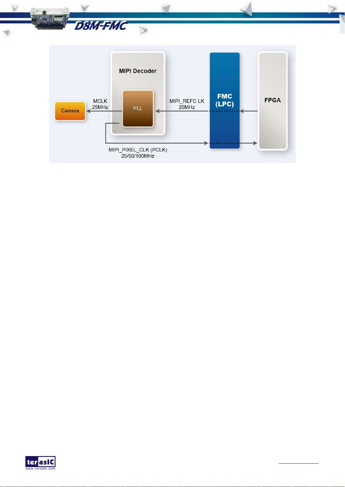
3.3 Clock Tree
Figure 3-4 is the D8M-FMC Board camera part‟s clock tree block diagram. MIPI Decoder PLL
receives FPGA Reference Clock (MIPI_REFCLK) and outputs Clock to Camera sensor (MCLK), at
the same time, MIPI Decoder PLL will also output a parallel port clock (MIPI_PIXEL_CLK) and
feedback to the FPGA to deal with parallel data.
D8M-FMC User
Manual
12
www.terasic.com
October 24, 2016
Figure 3-4 Simple Clock Tree of Camera part on D8M-FMC Board
In the provided demonstrations, MIPI_REFCLK is set to 20MHz; FPGA transmits this clock to the
D8M-FMC MIPI Decoder PLL through the FMC connector. No matter how much the camera
resolution is, the MCLK fixed output is 25MHz. According to the output resolution, MIPI_PIXEL_CLK
can be set as 25MHz for 640x480@60fps and 100MHz for 1920x1080@30fps.
For more MIPI Decoder PLL setting details, please refer to TC358746AXBG_748XBG_rev09.pdf
"Chapter 5: Clock and System" or refer to Terasic demonstrations.
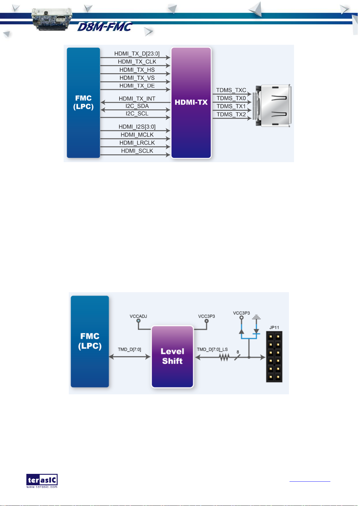
3.4 HDMI TX Interface
The development board provides High Performance HDMI Transmitter via the Analog Devices
ADV7513 which incorporates HDMI v1.4 features, including 3D video support, and 165 MHz supports
all video formats up to 1080p and UXGA. The ADV7513 is controlled via a serial I2C bus interface,
which is connected to pins on the FMC Connector.
Figure 3-5 Shows the connections of FMC LPC connector and HDMI TX chip.
D8M-FMC User
Manual
13
www.terasic.com
October 24, 2016
Figure 3-5 Connections between the FMC and HDMI Transmitter Chip
3.5 TMD Expansion Header
The development board provides a TMD (Terasic Mini Digital) expansion header, and pins of the
interface are shifted to 3.3V IO standard by a Level Shift. Users can use this TMD interface to extend
their own designs, and please make sure TMD_D [7:0] are general purpose IOs on the main board.
Figure 3-6 Shows the connections between FMC LPC connector and TMD expansion header.
Figure 3-6 Connections between the FMC and TMD expansion header

D8M-FMC User
Manual
14
www.terasic.com
October 24, 2016
3.6 FMC Connector
Figure 3-7,Figure 3-8 and Table 3-1 Shows the pin out and pin definitions of the FMC LPC
connector.
Figure 3-7 Pin-out of the FMC LPC connector on D8M-FMC (1)

D8M-FMC User
Manual
15
www.terasic.com
October 24, 2016
Signal Name
Connector
Pin No.
Description
Pin
Direction
I/O
Standard
CAMERA_I2C_SCL
G27
I2C Clock for MIPI camera
inout
VCCADJ
CAMERA_I2C_SDA
G28
I2C Data for MIPI camera
inout
VCCADJ
CAMERA_PWDN_n
C27
Power Down signal of MIPI camera
output
VCCADJ
CAMERA_RESV_PIN
D12
Reserve
output
VCCADJ
MIPI_CS_n
G25
Chip Select
output
VCCADJ
MIPI_I2C_SCL
G21
I2C Clock for bridge device
inout
VCCADJ
MIPI_I2C_SDA
G22
I2C Data for bridge device
inout
VCCADJ
MIPI_MCLK
D8
Reserve
output
VCCADJ
MIPI_PIXEL_CLK
G33
Parallel Port Clock signal
input
VCCADJ
MIPI_PIXEL_D[0]
G16
Parallel Port Data
input
VCCADJ
MIPI_PIXEL_D[1]
C14
Parallel Port Data
input
VCCADJ
MIPI_PIXEL_D[2]
C15
Parallel Port Data
input
VCCADJ
MIPI_PIXEL_D[3]
G15
Parallel Port Data
input
VCCADJ
MIPI_PIXEL_D[4]
G12
Parallel Port Data
input
VCCADJ
MIPI_PIXEL_D[5]
G13
Parallel Port Data
input
VCCADJ
MIPI_PIXEL_D[6]
C11
Parallel Port Data
input
VCCADJ
MIPI_PIXEL_D[7]
G10
Parallel Port Data
input
VCCADJ
MIPI_PIXEL_D[8]
G9
Parallel Port Data
input
VCCADJ
MIPI_PIXEL_D[9]
C10
Parallel Port Data
input
VCCADJ
MIPI_PIXEL_HS
C19
Parallel Port Horizontal
Synchronization signal
input
VCCADJ
Figure 3-8 Pin-out of the FMC LPC connector on D8M-FMC (2)
Table 3-1 Pin Assignment of D8M-FMC FMC Interface

D8M-FMC User
Manual
16
www.terasic.com
October 24, 2016
MIPI_PIXEL_VS
C18
Parallel Port Vertical
Synchronization signal
input
VCCADJ
MIPI_REFCLK
G18
Reference Clock Input of bridge
device
output
VCCADJ
MIPI_RESET_n
G24
Master Reset signal for MIPI
camera and bridge device
output
VCCADJ
HDMI_I2C_SCL
G31
HDMI I2C Clock
inout
VCCADJ
HDMI_I2C_SDA
G30
HDMI I2C Data
inout
VCCADJ
HDMI_I2S[0]
H35
I2S Channel 0 Audio Data Input
output
VCCADJ
HDMI_I2S[1]
D20
I2S Channel 1 Audio Data Input
output
VCCADJ
HDMI_I2S[2]
G36
I2S Channel 2 Audio Data Input
output
VCCADJ
HDMI_I2S[3]
H37
I2S Channel 3 Audio Data Input
output
VCCADJ
HDMI_LRCLK
H38
Left/Right Channel Signal Input
output
VCCADJ
HDMI_MCLK
D21
Audio Reference Clock Input
output
VCCADJ
HDMI_SCLK
G37
I2S Audio Clock Input
output
VCCADJ
HDMI_SPDIF
H34
S/PDIF Audio Input.
output
VCCADJ
HDMI_TX_CLK
D23
Video Clock
output
VCCADJ
HDMI_TX_D[0]
H29
Video Data bus
output
VCCADJ
HDMI_TX_D[1]
H28
Video Data bus
output
VCCADJ
HDMI_TX_D[2]
D27
Video Data bus
output
VCCADJ
HDMI_TX_D[3]
C26
Video Data bus
output
VCCADJ
HDMI_TX_D[4]
H26
Video Data bus
output
VCCADJ
HDMI_TX_D[5]
D26
Video Data bus
output
VCCADJ
HDMI_TX_D[6]
H25
Video Data bus
output
VCCADJ
HDMI_TX_D[7]
D24
Video Data bus
output
VCCADJ
HDMI_TX_D[8]
H23
Video Data bus
output
VCCADJ
HDMI_TX_D[9]
H22
Video Data bus
output
VCCADJ
HDMI_TX_D[10]
D18
Video Data bus
output
VCCADJ
HDMI_TX_D[11]
H20
Video Data bus
output
VCCADJ
HDMI_TX_D[12]
H19
Video Data bus
output
VCCADJ
HDMI_TX_D[13]
D17
Video Data bus
output
VCCADJ
HDMI_TX_D[14]
H17
Video Data bus
output
VCCADJ
HDMI_TX_D[15]
H16
Video Data bus
output
VCCADJ
HDMI_TX_D[16]
D15
Video Data bus
output
VCCADJ
HDMI_TX_D[17]
D14
Video Data bus
output
VCCADJ
HDMI_TX_D[18]
H14
Video Data bus
output
VCCADJ
HDMI_TX_D[19]
H13
Video Data bus
output
VCCADJ
HDMI_TX_D[20]
H11
Video Data bus
output
VCCADJ
HDMI_TX_D[21]
H10
Video Data bus
output
VCCADJ
HDMI_TX_D[22]
H8
Video Data bus
output
VCCADJ
HDMI_TX_D[23]
H7
Video Data bus
output
VCCADJ

D8M-FMC User
Manual
17
www.terasic.com
October 24, 2016
HDMI_TX_DE
H31
Data Enable Signal for Digital
Video.
output
VCCADJ
HDMI_TX_HS
H32
Horizontal Synchronization
output
VCCADJ
HDMI_TX_INT
G19
Interrupt Signal
input
VCCADJ
HDMI_TX_VS
G34
Vertical Synchronization
output
VCCADJ
CLK_12MHZ
D11
Reserve
output
VCCADJ
TMD_D[0]
C22
Terasic Mini Digital Data 0
inout
VCCADJ
TMD_D[1]
C23
Terasic Mini Digital Data 1
inout
VCCADJ
TMD_D[2]
G6
Terasic Mini Digital Data 2
inout
VCCADJ
TMD_D[3]
D35
Terasic Mini Digital Data 3
inout
VCCADJ
TMD_D[4]
H4
Terasic Mini Digital Data 4
inout
VCCADJ
TMD_D[5]
H5
Terasic Mini Digital Data 5
inout
VCCADJ
TMD_D[6]
G2
Terasic Mini Digital Data 6
inout
VCCADJ
TMD_D[7]
G3
Terasic Mini Digital Data 7
inout
VCCADJ

D8M-FMC User
Manual
18
www.terasic.com
October 24, 2016
Chapter 4
RTL Example Codes
This chapter provides instructions on how to capture a D8M-FMC image (resolution is 720P@60 Hz)
and use on-chip-ram storage methods to display the image on a HDMI Monitor. The storage methods
realized by pure Verilog HDL language have been validated on TR5, A10SoC and A10GFP board.
4.1 D8M-FMC RTL Demonstration Descriptions
This section provides instructions on how to store Camera capturing image(720P@60Hz)in a larger
on-chip memory(Frame-Buffer), this Memory is expect to store up to one Frame image, and how to
extract Frame-Buffer address data to convert RAW data to RGB data, and output the RGB data to
LCD with 720P@60 Hz timing.
Function Block Diagram
Figure 4-1 Shows the Function block diagram of Camera demonstration. This design block is one
dual-port-ram Control module can control on chip Memory and read/write image data. Camera raw
data will be written in on-chip-ram first. After finishing writing a Frame, ON-CHIP_FRAM module will
read out the data from dual-port-ram to RAW2RGB_J module to convert RAW data to RGB data. The
RGB data will output along with the signal timing generated by VGA_Controller to LCD. In the block,
other module (for example, FOCUS_ADJ, MIPI_BRIDGE_CAMERA_Config ) function instructions
and BUTTON/SW operation. All module functions are described below:
.

D8M-FMC User
Manual
19
www.terasic.com
October 24, 2016
Figure 4-1 Block diagram of the digital camera D8M-FMC design with on-chip memory
RESET_DELAY: When press BUTTON0 , this module will provide LOW signal of about 0.25 seconds
for the whole system module to do RESET.
ON_CHIP_FRAM :This module is one dual-port-ram controller can control 1280 x 720 x10bit on-chip
ram and read/write image data
MIPI_BRIDGE_CAMERA_Config :the MIPI BRIDGE I2C and Camera I2C setting controller, such as
set to output 720P@60Hz timing. It mainly writes I2C corresponding parameters to MIPI-BRIDGE
IC register and Camera Sensor IC register respectively through their own I2C buses. MIPI_I2C
bus is used to write MIPI BRIDGE I2C (I2C Slave Address = 0x1c.), CAMERA_I2C bus is used
to write Camera Sensor (IC Slave Address = 0x6c).
RAW2RGB_J : This module is to convert RAW data to RGB data.
VGA_Controller: the LCD signal timing generator, can generate 720P@60 Hz signal timing.
FOCUS_ADJ: This module provides two main functions.
The first function is using I2C bus to write D8M Voice Coil Motor (VCM) driver IC register, and
control the camera lens‟ movements to perform image focusing. VCM driver IC register (I2C Slave
Address =0x18) shares I2C bus with camera module. The other function is doing the current
image high frequency component statistic. When the VCM drives the camera lens‟ movement, a
real-time statistics of image high-frequency sum will be done in every step of the moving. Finally,
the lens will move to a position which has the largest number of high frequency to complete the
automatic focus operation.

D8M-FMC User
Manual
20
www.terasic.com
October 24, 2016
Focus area can be selected by SW3. There are two options:
(1). Select focusing the whole screen area (set SW3 to 0)
(2). Select focusing the middle area (set SW3 to 1).
Once you set SW3 to a value (0 or 1) and press BUTTON2 one time, the automatic focus operation
will be performed in the selected area.
GAMMA_CORRECT: by Bézier Curve in real time (none LUT-TABLE) produce GAMMA curve generate
new RGB's data.
HDMI_TX_AD7513: This module will setting AD7513 (HDMI TX) I2C setting controller, set register
respectively through own I2C buses. (I2C Slave Address = 0x72), and 1 KHz sine wave by I2S bus
send to AD7513 output sound.
CLOCKMEM: This module will divide MIPI_PIXEL_CLK (100MHz) to 1Hz to display on LEDs.
We provide the demonstrations on TR5, A10SoC and A10GFP. The section SWITCH setting and
BUTTON operation are the same on TR5, A10SoC and A10GFP. The following are the descriptions of
the three platforms‟ set up, as well as the test steps.
4.2 D8M-FMC RTL Demonstration on TR5
Hardware Setting Up
As shown in Figure 4-2
Figure 4-2 TR5 demo hardware setting up

D8M-FMC User
Manual
21
www.terasic.com
October 24, 2016
Name
Description
LED0
Lights up when MIPI DECODER I2C setting is successful
LED1
Lights up when CAMERA I2C setting is successful
LED2
When HDMI cable plug , LED Blink (blanking)
LED3
Blink in 1HZ (D8M-FMC PIXE CLOCK /100M)
BUTTON0
SYSTEM RESET
BUTTON2
Image auto focus(area based on SW3 selection)
SW3
0: No yellow box (focus on whole screen area)
1: There is a yellow box(focus on yellow box)
Design Tools
Quartus II v16.0
Demonstration Source Code
Quartus project directory: TR5_D8M_FMC_RTL
Bitstream used: D8M_FMC.sof
Demonstration Batch File
Demo batch file folder: demonstrations\TR5_D8M_FMC_RTL\demo_batch
Demonstration Setup
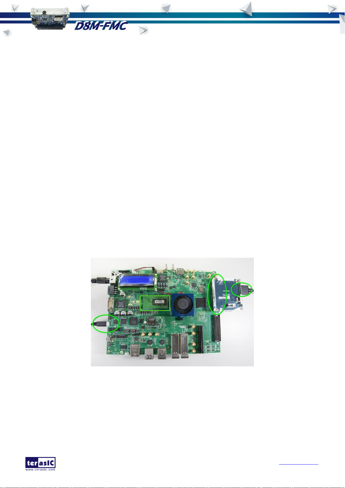
Connect the TR5 (J6) to the host PC with a USB cable and install the USB-Blaster II driver if
necessary.
Plug D8M-FMC onto TR5 FMC_D(J10), connect HDMI monitor to HDMI port see Figure 4-2.
Plug the 12V adapter to TR5 Board.
Make sure the VADJ of FMC_D is set to 2.5V by placing a jumper between JP9.7 and JP9.8,
as shown in Figure 4-4
Power on the TR5 board.
Execute the demo batch file “test.bat” from the directory\TR5_D8M_FMC_RTL\demo_batch.
LED0~1 light up, stand the settings of D8M-FMC MIPI decoder IC and Camera Sensor I2C
are completed..
LED2 when plug HDMI monitor cable generates an interrupt signal. LED2 will extinguish, and
after bright.
LED3 blink in 1Hz, stand MIPI_PIXEL_CLK are generated correctly.
D8M-FMC capturing image displays on HDMI monitor, if the HDMI monitor image is fuzzy,
please press BUTTON2 one time again (will perform the focus operation again). Users can
switch SW3 to “1” (there will be a yellow box on image), then, press BUTTON2 one time again,
the middle area focus operation will be performed.
This demonstration also simply demonstrates the HDMI-Audio function ,it will produce a 1K
sine wave voice when pressing BUTTON3.
Table 4-1 Summarizes the functional keys and details of each LED status.
Table 4-1 The functional keys of the TR5 digital camera demonstration

D8M-FMC User
Manual
22
www.terasic.com
October 24, 2016
Figure 4-3 Shows the locations of buttons/switches/LEDs on TR5 board.
Figure 4-3 Buttons/Swtiches/LEDs on TR5 Board
Figure 4-4 Adjust FMC_D VADJ to 2.5V by short JP9.7 and JP9.8

D8M-FMC User
Manual
23
www.terasic.com
October 24, 2016
4.3 D8M-FMC RTL Demonstration on A10SoC
Hardware Setting Up
As shown in Figure 4-5
Figure 4-5A10SoC demo hardware setting up
Design Tools
Quartus II v16.0
Demonstration Source Code
Quartus project directory: A10SOC_D8M_FMC_RTL
Bitstream used: A10SOC_D8M_FMC_RTL.sof
Demonstration Batch File
Demo batch file folder: Demonstrations\A10SOC_D8M_FMC_RTL\demo_batch
Demonstration Setup
Connect the A10SoC board (J22) to the host PC with a USB cable and install the USB-Blaster
II driver if necessary.
Plug D8M-FMC onto A10SoC (FMC Port A), connect HDMI monitor to HDMI port see
Figure 4-5
Plug the 12V adapter to A10SoC Board.
Make sure the FMC_A‟s VADJ is set to 1.8V by short J42.9 and J42.10 as shown in
Figure 4-8
Power on the A10SoC board.
Execute the demo batch file “test.bat” from the directory\
A10SOC_D8M_FMC_RTL\demo_batch.

D8M-FMC User
Manual
24
www.terasic.com
October 24, 2016
Name
Description
USER_LED_FPGA0(D26)
Lights up when MIPI DECODER I2C setting is successful
USER_LED_FPGA1(D25)
Lights up when CAMERA I2C setting is successful
USER_LED_FPGA2(D28)
When HDMI cable plug , LED Blink (blanking)
USER_LED_FPGA3(D27)
Blink in 1HZ (D8M-FMC PIXE CLOCK /100M)
USER_PB_FPGA0(PB0)
SYSTEM RESET
USER_PB_FPGA2(PB2)
Image auto focus(area based on DIPSW_FPGA3 selection)
USER_DIPSW_FPGA3(SW2.8)
0: No yellow box (focus on whole screen area)
1: There is a yellow box(focus on yellow box)
USER_LED_FPGA0~1 light up, stand the settings of D8M-FMC MIPI decoder IC and Camera
Sensor I2C are completed..
USER_LED_FPGA2 when plug HDMI monitor cable generates an interrupt signal.
USER_LED_FPGA2 will extinguish, and after bright.
USER_LED_FPGA3 blink in 1Hz, stand MIPI_PIXEL_CLK are generated correctly.
D8M-FMC capturing image displays on HDMI monitor, if the HDMI monitor image is fuzzy,
please press USER_PB_FPGA2 one time again (will perform the focus operation again). Users
can switch USER_DIPSW_FPGA3 to “1” (there will be a yellow box on image), then, press
USER_PB_FPGA2 one time again, the middle area focus operation will be performed.
This demonstration also simply demonstrates the HDMI-Audio function ,it will produce a 1K
sine wave voice when pressing USER_PB_FPGA2.
Table 4-2 Summarizes the functional keys and details of each LED status.
Table 4-2 The functional keys of the A10SoC digital camera demonstration
Figure 4-6 and Figure 4-7 Show the locations of buttons/switches/LEDs on A10SoC board:
Figure 4-6 USER_DIPSW_FPGA3 location on A10SoC board

D8M-FMC User
Manual
25
www.terasic.com
October 24, 2016
Figure 4-7 USER_PB_FPGA/USER_LED_FPGA locations on A10SoC board
Figure 4-8 Adjust FMC_A VADJ to 1.8V by short J42.9 and J42.10

D8M-FMC User
Manual
26
www.terasic.com
October 24, 2016
4.4 D8M-FMC RTL Demonstration on A10GFP
Hardware Setting Up
As shown in Figure 4-9
Figure 4-9 A10GFP demo hardware setting up
Design Tools
Quartus II v16.0
Demonstration Source Code
Quartus project directory: A10GFP_D8M_FMC_RTL.
Bitstream used: A10GFP_D8M_FMC_RTL.sof.
Demonstration Batch File
Demo batch file folder: Demonstrations\A10GFP_D8M_FMC_RTL\demo_batch
Demonstration Setup
Connect the A10GFP board (J3) to the host PC with a USB cable and install the USB-Blaster
II driver if necessary
Plug D8M-FMC onto A10GFP (FMC Port A), connect HDMI monitor to HDMI port of D8M-FMC
see Figure 4-9.
Plug the 12V adapter to A10GFP Board.
Make sure the FMC_A‟s VADJ is set to 1.8V by short R1086 as shown in Figure 4-11.(The
A10GFP version is Rev E3.1)
Power on the A10GFP board.
Execute the demo batch file “test.bat” from the directory\

D8M-FMC User
Manual
27
www.terasic.com
October 24, 2016
Name
Description
USER_LED_R0 (D10)
Lights up when MIPI DECODER I2C setting is successful
USER_LED_R1 (D9)
Lights up when CAMERA I2C setting is successful
USER_LED_R2 (D8)
When HDMI cable plug , LED Blink (blanking)
USER_LED_R3 (D7)
Blink in 1HZ (D8M-FMC PIXE CLOCK /100M)
USER_PB0 (PB0)
SYSTEM RESET
USER_PB2 (PB2)
Image auto focus(area based on USER_DIPSW3 selection)
USER_DIPSW3(SW2.4)
0: No yellow box (focus on whole screen area)
1: There is a yellow box(focus on yellow box)
A10GFP_D8M_FMC_RTL\demo_batch.
USER_LED_R0~1 light up, stand the settings of D8M-FMC MIPI decoder IC and Camera
Sensor I2C are completed..
USER_LED_R2 when plug HDMI monitor cable generates an interrupt signal. USER_LED_R2
will extinguish, and after bright.
USER_LED_R3 blink in 1Hz, stand MIPI_PIXEL_CLK are generated correctly.
D8M-FMC capturing image displays on HDMI monitor, if the HDMI monitor image is fuzzy,
please press USER_PB2 one time again (will perform the focus operation again). Users can
switch USER_DIPSW3 to “1” (there will be a yellow box on image), then, press USER_PB2 one
time again, the middle area focus operation will be performed.
This demonstration also simply demonstrates the HDMI-Audio function ,it will produce a 1K
sine wave voice when pressing USER_PB2.
Table 4-3 Summarizes the functional keys and details of each LED status.
Table 4-3 The functional keys of the A10GFP digital camera demonstration
Figure 4-10 Shows the locations of buttons/switches/LEDs on A10GFP board:
Figure 4-10 USER PBs/DIPSWs/LEDs locations on A10GFP board

D8M-FMC User
Manual
28
www.terasic.com
October 24, 2016
Figure 4-11 Adjust FMC_A VADJ to 1.8V (default) by short R1086

D8M-FMC User
Manual
29
www.terasic.com
October 24, 2016
Chapter 5
NIOS Based Example Codes
This chapter provides several NIOS based examples for users to get started using the D8M-FMC
Board.
5.1 D8M-FMC VIP Demonstration on TR5
This demonstration shows how to implement a D8M-FMC on a TR5 FPGA Board. The Altera VIP
(Video Image Processing) suite is used to display images on the HDMI monitor. The Nios II
processor is used to configure the I2C devices. There is a Camera10 IP, from Terasic in Qsys, which
translates the 10-bits Bayer Pattern from the camera to the 30-bit RGB video stream format and
feeds it to the Altera VIP. The other IP developed by Terasic for auto-focus is used to find the
optimized focus settings of the user-defined image area.
Function Block Diagram
Figure 5-1 Block diagram of D8M-FMC VIP demonstration on TR5 shows the block diagram of
D8M-FMC VIP demonstration on the TR5 Board. The two I2C master controllers are used to
configure the camera module and MIPI-decoder in the D8M-FMC. The first I2C controller is used to
configure the camera module, including the OV8865 image sensor and the VCM149C. The second
I2C controller is used to configure the MIPI Decoder TC358748XBG.
Note: The focus driver IC (VCM149C) in the camera module is also configured by the Terasic
auto-focus IP through its own I2C master controller. Users must make sure there is only one I2C
master used one at a time.
The two GPIO controllers are used to retrieve the status of Buttons and Switches. The Histogram
controller is used to build the histogram data for the 10-bit Bayer Pattern from the camera module.
The image quality can be enhanced based on the analysis of histogram data. These controllers are
all controlled by the NIOS II processor. The NIOS II program is stored in the On-Chip memory. The
DDR3 controller is used to provide AVMM access interface for the DDR3-SODMM so the frame
buffer in the VIP Process block can use DDR3 as video memory.

D8M-FMC User
Manual
30
www.terasic.com
October 24, 2016
Figure 5-1 Block diagram of D8M-FMC VIP demonstration on TR5
The VIP Process contains a set of VIP as shown in Figure 5-5. In this demonstration, the Camera
is configured to generate a 10-bit 1920x1080 pixel Bayer pattern. The Terasic CAMRA10 IP is used
to convert the Bayer Pattern into a 1920x1080 30-bit RGB Altera VIP video stream. The Gamma
Corrector is an Altera VIP. It is used to re-map the RGB video to get an enhanced video based on a
1024-entry LUT (Loop Up Table). The Terasic Autofocus is used to automatically find the proper
focus position for the camera lens. The framebuffer is used to store the complete video frame for
display later. The framebuffer uses the external DDR3-SO-DIMM as video memory. The Clock Video
Output IP will translate the video stream to a 1920x1080 VGA format so the video can be displayed
on the HDMI monitor.
Figure 5-2 Block diagram of D8M-FMC VIP demonstration on TR5

D8M-FMC User
Manual
31
www.terasic.com
October 24, 2016
Image Process
In this demonstration, the Altera Gamma Corrector VIP is used to remap the RGB value to get an
enhanced value. The required LUT is calculated on NIOS II program based on the histogram data
retrieved from the HISTOGRAM IP. In this demonstration, three enhanced methods are
implemented:
Histogram Equalization
Histogram Stretching based on the highlight/shadow of current video frame
Histogram Stretching based on fixed highlight/shadow
The Histogram Equalization is to remap the pixel level such that each gray level has the same
intensity as shown in Figure 5-3.
Figure 5-3 Histograms of an image before and after equalization
The histogram stretching is to stretch the histogram so the highlight and shadow is mapped to
maximal and minimal pixel level. Figure 5-4 shows a histogram stretch example for 8-bit gray salve
image. The shadow point in the image will be remapped from 84 to 0, and the highlight point in the
image will be remapped from the 153 to 255.
Figure 5-4 Histogram Stretch
Beside, Gamma encoding also implemented in this demonstration for the nonlinear feature of HDMI
monitor. The Gamma LUT built by the following gamma encoding formula:

D8M-FMC User
Manual
32
www.terasic.com
October 24, 2016
The default camera settings
In this demonstration, the default camera settings are:
Resolution: 1920x1080
Frame Rate: 30 fps
Pixel Data: RAW10
Bin Mode: 1
Users can change the settings base on their requirements.
Design Tools
Quartus II v16.0.2 Standard Build 222
Nios II Eclipse 16.0.2
Demonstration Source Code
Quartus project directory: TR5_D8M_FMC_VIP
Nios II Eclipse project workspace: TR5_D8M_FMC_VIP\software
Demonstration Batch File
Demo batch file folder: demonstrations\TR5_D8M_FMC_VIP \demo_batch
Demonstration Setup
Install D8M-FMC Board on the FMC_D(J10) connector of TR5 and make sure the screw is
locked (See Figure 5-5)
Connect the HDMI connector on the D8M-FMC to a HDMI monitor (See Figure 5-5)
Connect a USB cable between the host PC and the USB connector (J6) on the TR5 board
(See Figure 5-5)
Make sure DDR3-SODMM is installed on the TR5
Make sure the VADJ of FMC_D is set to 2.5V by placing a jumper between JP9.7 and JP9.8,
as shown in Figure 5-6
Power on the TR5 board
Execute the demo batch file “test.bat” under the batch file folder
TR5_D8M_FMC_VIP\demo_batch
The HDMI Monitor will start showing the video captured from the camera as shown in Figure
5-7
LED indicators:
o LED0:DDR3 init pass
o LED1:DDR3 init done
o LED2:DDR3 cal success
o LED3:DDR3 cal fail
Control Focus:
o Press BUTTON0 to trigger the auto-focus function
o Press BUTTON1 to „ - ‟ adjust focus position in manual-focus
o Press BUTTON2 to „ + ‟ adjust focus position in manual-focus

D8M-FMC User
Manual
33
www.terasic.com
October 24, 2016
LUT(Loop Up Table) Image Process:
o SW1/SW0 = DOWN/DOWN. No image process is applied
o SW1/SW0 = DOWN/UP. Apply histogram equalization image process
o SW1/SW0 = UP/DOWN. Apply histogram stretching
o SW1/SW0 = UP/UP. Apply histogram stretching with fixed highlight/shadow
Gamma Encoding:
o SW2 = DOWN. No gamma encoding.
o SW2 = UP. Apply gamma encoding.
This demonstration also simply demonstrates the HDMI-Audio function ,it will produce a 1K
sine wave voice when pressing BUTTON3.
Figure 5-5 Setup TR5_D8M_FMC_VIP demonstration
Figure 5-6 Adjust FMC_D VADJ to 2.5V by short JP9.7 and JP9.8

D8M-FMC User
Manual
34
www.terasic.com
October 24, 2016
Figure 5-7 TR5_D8M_FMC_VIP demonstration running on TR5
5.2 D8M-FMC VIP Demonstration on Altera A10SoC
This demonstration shows how to implement a D8M-FMC on an Altera A10SoC FPGA Board. The
demonstration code is almost as same as the one used for the TR5. The block diagram is also the
same as the one used in the TR5 with the exception that the DDR3 controller is replaced by the
DDR4 controller and the DDR3-SODMM is replaced by the DDR4 module. The image process and
camera settings are the same as those used in TR5.
Design Tools
Quartus II v16.0.2 Standard Build 222
Nios II Eclipse 16.0.2
Demonstration Source Code
Quartus project directory: A10SoC_D8M_FMC_VIP
Nios II Eclipse project workspace: A10SoC_D8M_FMC_VIP\software
Demonstration Batch File
Demo batch file folder: demonstrations\A10SoC_D8M_FMC_VIP\demo_batch
Demonstration Setup
Install D8M-FMC Board on the FMC_A(J29) connector of A10SoC and make sure the screw is
Connect the HDMI connector on the D8M-FMC to a HDMI monitor (See Figure 5-8)
Connect a USB cable between the host PC and the USB connector (J22) on the A10SoC
Make sure DDR4 module is installed on the A10SoC
Make sure the FMC_A‟s VADJ is set to 1.8V by short J42.9 and J42.10 as shown in Figure
Power on the A10SoC board
locked (See Figure 5-8)
board (See Figure 5-8)
5-9
D8M-FMC User
Manual
35
www.terasic.com
October 24, 2016
Execute the demo batch file “test.bat” under the batch file folder
A10SoC_D8M_FMC_VIP\demo_batch
The HDMI Monitor will start showing the video captured from the camera as shown in
Figure 5-10
Use push buttons and DIP switches, as shown Figure 5-11, to perform various functions.
LED indicators:
o LED0:DDR4 init pass
o LED1:DDR4 cal success
o LED2:DDR4 cal fail
Control Focus:
o Press Push Button 0 to trigger the auto-focus function
o Press Push Button 1 to „ - ‟ adjust focus position in manual-focus
o Press Push Button 2 to „ + ‟ adjust focus position in manual-focus
LUT(Loop Up Table) Image Process:
o DIP Switch-SW0/ SW1 = DOWN/DOWN. No image process is applied
o DIP Switch-SW0/ SW1 = DOWN/UP. Apply histogram equalization image process
o DIP Switch-SW0/ SW1 = UP/DOWN. Apply histogram stretching
o DIP Switch-SW0/ SW1 = UP/UP. Apply histogram stretching with fixed
highlight/shadow
Gamma Encoding:
o DIP Switch -SW2 = DOWN. No gamma encoding.
o DIP Switch -SW2 = UP. Apply gamma encoding.
This demonstration also simply demonstrates the HDMI-Audio function ,it will produce a 1K
sine wave voice when pressing Push Button 2.
Figure 5-8 Setup A10SoC_D8M_FMC_VIP demonstration

D8M-FMC User
Manual
36
www.terasic.com
October 24, 2016
Figure 5-9 Adjust FMC_A VADJ to 1.8V by short J42.9 and J42.10
Figure 5-10 A10SoC_D8M_FMC_VIP demonstration running on A10SoC
Figure 5-11 Push Button and DIP Switch

D8M-FMC User
Manual
37
www.terasic.com
October 24, 2016
5.3 D8M-FMC VIP Demonstration on Altera A10GFP
This demonstration shows how to implement a D8M-FMC on an Altera A10GFP FPGA Board. The
demonstration code is almost as same as the one used TR5. The block diagram is also the same as
the one used in TR5 except the DDR3 controller is replaced by the DDR4 controller and the
DDR3-SODMM is replaced by DDR4 module. The image process and camera setting are the same
as those used in TR5.
Design Tools
Quartus II v16.0.2 Standard Build 222
Nios II Eclipse 16.0.2
Demonstration Source Code
Quartus project directory: A10GFP_D8M_FMC_VIP
Nios II Eclipse project workspace: A10GFP_D8M_FMC_VIP\software
Demonstration Batch File
Demo batch file folder: demonstrations\A10GFP_D8M_FMC_VIP\demo_batch
Demonstration Setup
Install D8M-FMC Board on the FMC_A(J1) connector of A10GFP and make sure the screw is
locked (See Figure 5-12)
Connect the HDMI connector on the D8M-FMC to a HDMI monitor (See Figure 5-12)
Connect a USB cable between the host PC and the USB connector (J3) on the A10GFP board
(See Figure 5-12)
Make sure DDR4 module is installed on the A10GFP
Make sure the FMC_A‟s VADJ is set to 1.8V by short R1086 as shown in Figure 5-13. (The
A10GFP version is Rev E3.1)
Power on the A10GFP board
Execute the demo batch file “test.bat” under the batch file folder
A10GFP_D8M_FMC_VIP\demo_batch
The HDMI Monitor will start showing the video captured from the camera as shown in Figure
5-14
Use push buttons and DIP switches, as shown Figure 5-15, to perform various functions
LED indicators:
o LED0:DDR4 init pass
o LED1:DDR4 cal success
o LED2:DDR4 cal fail
Control Focus:
o Press Push Button 0 to trigger the auto-focus function
o Press Push Button 1 to „ - ‟ adjust focus position in manual-focus
o Press Push Button 2 to „ + ‟ adjust focus position in manual-focus
LUT(Loop Up Table) Image Process:
o DIP Switch-SW0/ SW1 = DOWN/DOWN. No image process is applied

D8M-FMC User
Manual
38
www.terasic.com
October 24, 2016
o DIP Switch-SW0/ SW1 = DOWN/UP. Apply histogram equalization image process
o DIP Switch-SW0/ SW1 = UP/DOWN. Apply histogram stretching
o DIP Switch-SW0/ SW1 = UP/UP. Apply histogram stretching with fixed
highlight/shadow
Gamma Encoding:
o DIP Switch-SW2 = DOWN. No gamma encoding.
o DIP Switch-SW2 = UP. Apply gamma encoding.
This demonstration also simply demonstrates the HDMI-Audio function ,it will produce a 1K
sine wave voice when pressing Push Button 2.
Figure 5-12 Setup A10SoC_D8M_FMC_VIP demonstration
Figure 5-13 Adjust FMC_A VADJ to 1.8V (default) by short R1086

D8M-FMC User
Manual
39
www.terasic.com
October 24, 2016
Figure 5-14 A10SoC_D8M_FMC_VIP demonstration running on A10SoC
Figure 5-15 Push Button and DIP Switch

D8M-FMC User
Manual
40
www.terasic.com
October 24, 2016
Version
Change Log
V1.0
Initial Version
Revision History
Copyright Statement
Copyright © 2016 Terasic Inc. All rights reserved.
Chapter 6
Appendix
 Loading...