


M100 Datasheet
Version 0.1
Release Date 2017-07-05
Tel:+86-21-52242515 1 / 18

DocumentVersion
Chapter
01
The document only for following list module:
M100-QVCX-2G16G, M100-OVCX-1G8G, M100-OVCX-2G16G, M100-OVWX-1G8G,
M100-OVWX-2G16G, M100-OVTX-1G8G, M100-OVTX-2G16G,M100-QVCX-1G8G,
M100-QVCX-2G16G, M100-QVWX-1G8G, M100-QVWX-2G16G, M100-QVTX-1G8G,
M100-QVTX-2G16G, M100-OWNX-1G8G, M100-OWNX-2G16G, M100-QWNX-1G8G,
M100-QWNX-2G16G
Revision History
Date
2017-07-05
Descriptions
Creation
Tel:+86-21-52242515 2 / 18

1 Product Application Overview
M100 is a Android inside All wireless mode module. Now it Integrate with
LTE//HSDPA/HSUPA/WCDMA/EVDO/CDMA2000/GSM, Bluetooth, WIFI, GPS on board.
This document defines the M100 module and describes its air interface and hardware interface
within your application.
This document can help you to quickly understand module interface specifications, electrical and
mechanical details as well as other related information of M100 module. Associated with
application notes and user guide, you can use M100 module to design and set up devices
applications easily.
Figure: Framework of M100 Application
Tel:+86-21-52242515 3 / 18

General Info
Description
Features
Dimension
41x52.7x3.2mm
Weight
Total Pins
Processors
DRAM Memory Inside
Flash Memory Inside
Graphics
mali-T720 @ 450 MHz
OpenGL ES 1.1/2.0/3.0
OpenCL 1.0/1.1/1.2
DirectX9
Mobile
Dual SIM Dual Standby(DSDS)
Power supply
3.3 V to 4.2V (typical: 3.8V)
Temperature range
-40°C to 85°C
Humidity
5%~ 95%
Drop Height
1.5 meters, 6 free fall
RF Support
RF Band
2 Brief description
M100 Android world mode communication module
16g
162
Quad-core ARM® 1.3Ghz/Octa-core ARM® 1.5Ghz Cortex-A53
32KB L1 I-cache and 32KB L1 D-cache
512KB unified L2 cache
2GB LPDDR-3 Up to 667Mhz
8/16GB eMMC
Tel:+86-21-52242515 4 / 18
LTE FDD -B1/B2/B3/B4/B5/B7/B8/B20
LTE TDD -B41
WCDMA -B1/B2/B5/B8
TD-SCDMA -B34/B39
GSM -800/900/1800/1900
CDMA -BC0/BC1
Air Symbol Rate
LTE FDD -Cat4 DL 150Mbps/UL 50Mbps
Resolution
Displays
Primary Camera
MIPI CSI interface (4 data lanes)
13MP@30fps
Secondary Camera
MIPI CSI interface (4 data lanes)
13MP@30fps
Video
Decoder:
H.264 BP/MP/HP-1080p@30fps/40Mbps
MPEG-4 SP/ASP -1080p@30fps/40Mbps
H.263 -1080p@30fps/40Mbps
DivX 4x/5x/6x -1080p@30fps/40Mbps
DivX HD/XVID -1080p@30fps/40Mbps
Encoder:
H.264 High profile 1080p @30fps
Audio
LTE TDD -Cat4 DL 150Mbps/UL 50Mbps
WCDMA -HSDPA,HSUPA
-DL 42.2Mbps/UL 11.5Mbps
TD-SCDMA -DL 2.8Mbps/UL 2.2Mbps
GSM -GPRS DL 85.6kbps/UL 85.6kbps
-EDGE Classs12 DL 236.8kbps/UL 236.8kbps
CDMA/EVDO BC0/BC1 -DL 3.1Mbps/UL 1.8Mbps
Multimedia Description
Portrait panel resolution up to FHD (1,920*1,080)
MIPI DSI interface (4 data lanes)
Extended support (HDMI/LVDS)by used external chip
Audio content sampling rates supported:8kHz to 192kHz
Audio content sample formats supported: 8-bit/16-bit/24-bit,
Support Mono/Stereo output
External CODEC I2S interface supports 16-bit/24-bit,
Tel:+86-21-52242515 5 / 18
Audio encoding: AMR-NB, AMR-WB, AAC, OGG, ADPCM
Audio decoding: WAV, MP3, MP2, AAC,AMR-NB, AMR-WB, IDI,
Vorbis, APE,AAC-plus v1, AAC-plus v2, FLAC, WMA,ADPCM

Connectivity
Description
WLAN
802.11 /b/g/n
Security: WFA WPA/WPA2 personal,WPS2.0, WAPI (hardware)
Max data Rates 802.11n 40Mhz/150Mbps
Bluetooth
Bluetooth v4.0 Low Energy (LE) Compatible 2.1+EDR/3.0+HS
GPS
GPS/Glonass/Beidou/Galileo dual-band reception concurrently
Supports SBAS (Satellite-Based Augmentation Systems)-
WAAS/MSAS/EGNOS/GAGAN
NFC
By add on another module to support
FM
Extensional I/O
Other Input/Output
Description
Power down
105uA
Standby Without SIM
2.6mA
Standby with SIM
4.6mA
Mp3 play on back
98 mA
H.264 play
253mA
LTE video play
385mA
65-108MHz with 50kHz step
RDS/RBDS
Other Input/Output Description
Low speed: I2C/SPI/SPI/SD/ UART/I2S/SIM/Keypad/GPIO
High speed: MIPI LCD/MIPI Camera/USB
Analog: MIC/Speaker/Receiver/Headset/ADC
Tel:+86-21-52242515 6 / 18

3 Interface Overview
M100 Module show as the picture:
SRCLKENAI
UTXD2_RTS
IDDIG
CAM_PDN1
CAM_PDN0
CAM_RST1
URXD2
UTXD2
KCOL0
KCOL1
KCOL2
CMMCLK
VBATSENSE
KROW2
KROW1
KROW0
GND
C2K_ANT
GND
USPI_MI
USPI_MO
USPI_CK
USPI_CS
SD_EINT
NFC_IRQ
NFC_RST
NFC_EINT
NFC_ENB
SDA3
SCL3
I2S1_LRCK
I2S1_DO
I2S1_BCK
VSIM2
SIM_INT2
SIM2_IO
SIM2_CLK
SIM2_RST
VSIM1
SIM_INT1
SIM1_IO
SIM1_CLK
SIM1_RST
DSI_TE
AUX_IN2
LCM_RST
GND
PRX_ANT
GND
PWRKEY
HO
ME
KEY
DISP_PWM
VBAT
UTXD2_CTS
URXD0
UTXD0
USB_DRV
GND
VBAT
A
LPS_EINT
GY_E
SDA2
SCL2
INT
117 118 119 120 121 122 123 124 125 126 127 128 129 130 131 132 133 134 135 136 137 138 139 140 141 142 143 144 145 146 147 148 149 150 151 152 153 154 155 156 157 158 159 160 161 162
116
115
114
113
112
111
110
109
108
107
106
105
104
103
102
101
100
99
98
97
96
95
94
93
92
91
90
89
88
87
86
85
84
83
82
VRTC
VIBR
VIO18
VIO28
CMMCLK1
SDA0
SCL0
Bott
VBUS
CHR_LDO
ISENSE
FLASH_STROBE
CAM_RST0
FLASH_EN
GND
om Vi
GND
KEY_LED
ISINK1
VDRV
RDN3_A
RDN2_A
RDN1_A
RDP2_A
RDP1_A
ew
CS_N
VBAT
RDN0_A
RDP0_A
RCN_A
RCP_A
RDN3
RDN2
RDN1
GND
AU_HSN
SPK_P
SPK_N
GND
CS_P
RDP3
GND
HP_MICP
AU_HPL
AU_HPR
EAR_EINT
AU_HSP
RDN0
RDP2
RDP1
RDP0
GND
RCN
RCP
1
GN
D
2
WI
ANT
FI_
3
GND
4
FM_ANT
5
FM_ANT_N
6
SDA1
7
SCL1
8
CTP_RSTB
9
CTP_EINT
10
GND
11
TDP2
12
TDN2
13
TDP1
14
TDN1
15
TDP3
16
TDN3
17
TDP0
18
TDN0
19
TCP
20
TCN
21
TF_CMD
22
TF_CLK
23
TF_D0
24
TF_D1
25
TF_D2
26
TF_D3
27
USB_DM
28
USB_DP
29
VCAMD
30
VCAMIO
31
VTF
32
VCAMAF
33
VCTP
34
VCAMA
35
AUDIO_REF
36373839404142434445464748495051525354555657585960616263646566676869707172737475767778798081
M
MICP0
MICN0
MICP1
MICN1
MICBIAS0
GND
HP_MICN
ICB
RDP3_A
VBAT
BAT_ON
GND
IAS1
Figure: Pin Bottom view of M100 module
The following figure shows a block diagram of M100 and illustrates the major functional parts.
Tel:+86-21-52242515 7 / 18

Figure: Functional Diagram
◇
Storage
1
ROM (EMMC)
16GB
2
RAM (LPDDR3)
2GB
◇
Wireless
1
Bluetooth
BT4.0 with A2DP / BLE
2
Wi-Fi
802.11
3
GPS
Global Position System
NFC
FM
Interface
All Interface for user application detail show as following:
Table 1 :M100 hardware interface total view
4
5
◇
Tel:+86-21-52242515 8 / 18
Support by external NFC module
FM onboard

1
USB with OTG
USB high speed 2.0
2
Storage Card
UHS SD3.0
3
I2C
x4
4
UART
x3
5
I2S
x1
6
SPI
x1
7
DPI(RGB LCD)
x1
8
DSI(MIPI LCD)
x1
9
CSI(CAMERA)
x2
GPIO
11
SIM
x2
MIC
13
Headset
x1
Receiver
Speaker
Keypad
LED
18
ADC
x1
19
RTC
x1
20
ANT
x3
21
FM ANT
x2
10
12
14
15
16
17
x2
x1
x1
3x3x2
x2
Tel:+86-21-52242515 9 / 18

No.
PinName
Type
Description
1
GND
VSS
Ground
2
WIFI_ANT
Antenna
WIFI Antenna
3
GND
VSS
Ground
4
FM_ANT
Antenna
FM Antenna Positive
FM_ANT_N
SDA1
SCL1
CTP_RSTB
CTP_EINT
GND
TDP2
TDN2
13
TDP1
LVDS ouput
Display LCD MIPI output DP1
14
TDN1
LVDS ouput
Display LCD MIPI output DN1
15
TDP3
LVDS ouput
Display LCD MIPI output DP3
16
TDN3
LVDS ouput
Display LCD MIPI output DN3
17
TDP0
LVDS ouput
Display LCD MIPI output DP0
18
TDN0
LVDS ouput
Display LCD MIPI output DN0
19
TCP
LVDS ouput
Display LCD MIPI output clock P
20
TCN
LVDS ouput
Display LCD MIPI output clock N
21
TF_CMD
CMOS
input/output
Storage card command
22
TF_CLK
CMOS
input/output
Storage card clock
23
TF_D0
CMOS
input/output
Storage card data 0
24
TF_D1
CMOS
input/output
Storage card data 1
25
TF_D2
CMOS
input/output
Storage card data 2
26
TF_D3
CMOS
input/output
Storage card data 3
USB_DM
USB_DP
VCAMD
4 Interface description
Table 2:M100 pin description
5
6
7
8
9
10
11
12
Antenna FM Antenna negative
Open drain I2C1 data
Open drain
Bi-Directional
Bi-Directional
VSS
LVDS ouput Display LCD MIPI output DP2
LVDS ouput Display LCD MIPI output DN2
I2C1 clock
GPIO
GPIO
Ground
27
28
29
Tel:+86-21-52242515 10 / 18
LVDS input/ouput USB 2.0 DM
LVDS input/ouput USB 2.0 DP
Power output
Camera Digital Power

No.
PinName
Type
Description
30
VCAMIO
Power output
Camera IO Power
31
VTF
Power output
SD Card Power
32
VCAMAF
Power output
Camera Auto Focus Power
33
VTP
Power output
Touch IC Power
34
VCAMA
Power output
Camera Analog Power
35
AUDIO_REF
Analog input
Audio Reference Ground
36
MICBIAS1
Power output
Headset MIC bias
37
MICP0
Analog input
MIC input 1+
38
MICN0
MICP1
MICN1
41
MICBIAS0
Power output
Main MIC bias
GND
HP_MICN
HP_MICP
AU_HPL
46
AU_HPR
Analog output
Headset Audio Right Output -
47
EAR_EINT
CMOS
input/output
Headset Insert Interrupt Input
48
AU_HSP
Analog output
Audio Receiver +
49
AU_HSN
Analog output
Audio Receiver -
50
SPK_P
Analog output
Audio Speaker +
51
SPK_N
Analog output
Audio Speaker -
52
GND
VSS
Ground
53
CS_P
Analog input
Coulomb Counter +
54
CS_N
Analog input
Coulomb Counter -
55
VBAT
Power intput
Battery Input Power 3.4~4.2V
56
VBAT
Power intput
Battery Input Power 3.4~4.2V
57
BAT_ON
Analog input
Battery Temperature Detection
58
GND
VSS
Ground
59
GND
VSS
Ground
60
KEY_LED
LED Sink
Keypad Backlight Sink
61
ISINK1
LED Sink
LED Sink
62
VDRV
Analog output
Charger Drive
63
VBUS
Analog input
USB VBUS
CHR_LDO
ISENSE
VBATSENSE
Analog input
MIC input 1-
39
40
42
43
44
45
Analog input MIC input 2+
Analog input MIC input 2-
VSS Ground
Analog input
Analog input
Analog output
Headset MIC Input Headset MIC Input +
Headset Audio Left Output -
64
65
66
Tel:+86-21-52242515 11 / 18
Analog output Charger LDO For Detect
Analog input Charger Current Sensor-
Analog input
Charger Current Sensor+

No.
PinName
Type
Description
67
KROW2
Digital input/output
Matrix Keypad Row2
68
KROW1
Digital input/output
Matrix Keypad Row1
69
KROW0
Digital input/output
Matrix Keypad Row0
70
KCOL0
Digital input/output
Matrix Keypad Col0
71
KCOL1
Digital input/output
Matrix Keypad Col1
72
KCOL2
Digital input/output
Matrix Keypad Col2
73
IDDIG
Digital input/output
OTG ID
74
USB_DRV
Analog output
Charge Drive
GND
VBAT
VBAT
VRTC
VIBR
VIO18
VIO28
HOMEKEY
83
PWRKEY
Digital input
Power On/Off Key
84
GND
VSS
Ground
85
PRX_ANT
Antenna
LTE/3G/2G Main Anatenna
86
GND
VSS
87
LCM_RST
Digital input/output
LCM Reset
88
AUX_IN2
Analog input
Aux Adc Input
89
DSI_TE
Digital input/output
Display Enable
90
SIM1_RST
Digital input/output
SIM Card 1 Reset
91
SIM1_CLK
Digital input/output
SIM Card 1 Clock
92
SIM1_IO
Digital input/output
SIM Card 1 I/O
93
SIM_INT1
Digital input/output
SIM Card 1 Interrupt
94
VSIM1
Power output
SIM Card 1 Power
95
SIM2_RST
Digital input/output
SIM Card 2 Reset
96
SIM2_CLK
Digital input/output
SIM Card 2 Clock
97
SIM2_IO
Digital input/output
SIM Card 2 I/O
98
SIM_INT2
Digital input/output
SIM Card 2 Interrupt
99
VSIM2
Power output
SIM Card 2 Power
100
I2S1_BCK
Digital input/output
I2S1 BCK
I2S1_DO
I2S1_LRCK
SCL3
75
76
77
78
79
80
81
82
VSS
Power intput
Battery Input Power 3.4~4.2V
Power intput Battery Input Power 3.4~4.2V
Power output Real Time Clock Power
Power output
Power output
Power output
Digital input
Vibrator Power
1.8V IO Power
2.8V IO Power
Home Key
101
102
103
Tel:+86-21-52242515 12 / 18
Digital input/output I2S1 DO
Digital input/output I2S1 LRCK
Open drain
I2C3

No.
PinName
Type
Description
104
SDA3
Open drain
I2C3
105
NFC_ENB
Digital input/output
General GPIO
106
NFC_EINT
Digital input/output
General GPIO
107
NFC_RST
Digital input/output
General GPIO
108
NFC_IRQ
Digital input/output
General GPIO
109
SD_EINT
Digital input/output
General GPIO
110
USPI_CS
Digital input/output
General GPIO
111
USPI_CK
Digital input/output
General GPIO
112
USPI_MO
USPI_MI
GND
C2K_ANT
GND
GY_EINT
ALPS_EINT
119
SDA2
Open drain
I2C2
120
SCL2
Open drain
I2C2
121
DISP_PWM
Digital input/output
General GPIO
122
URXD0
Digital input/output
UART 0 RXD
123
UTXD0
Digital input/output
UART 0 TXD
124
UTXD2_CTS
Digital input/output
UART 2 CTS
125
UTXD2_RTS
Digital input/output
UART 2 RTS
126
URXD2
Digital input/output
UART 2 RXD
127
UTXD2
Digital input/output
UART 2 TXD
128
SRCLKENAI
Digital input
NFC Clock Request
129
CAM_PDN1
Digital input/output
Camera Power Down 0/GPIO
130
CAM_PDN0
Digital input/output
Camera Power Down 1/GPIO
131
CAM_RST1
Digital input/output
Camera Power Reset 1/GPIO
132
CMMCLK
Digital clock output
Camera 0 Main Clock Output
133
CMMCLK1
Digital clock output
Camera 1 Main Clock Output
134
SCL0
Open drain
I2C0
135
SDA0
Open drain
I2C0
136
FLASH_EN
Digital input/output
Camera 0 Main Flash LED Enable
FLASH_STROBE
CAM_RST0
Digital input/output
General GPIO
113
114
115
116
117
118
Digital input/output
VSS Ground
Antenna
VSS
Digital input/output
Digital input/output
General GPIO
LTE/3G Aux Antenna,CDMA Main
Antenna
Ground
General GPIO
General GPIO
137
138
Tel:+86-21-52242515 13 / 18
Digital input/output
Digital input/output
Camera 0 Main Flash Strobe Enable
Camera Power Reset 0/GPIO

No.
PinName
Type
Description
139
GND
VSS
Ground
140
RDP3_A
LVDS input
Camera1 MIPI IN3+
141
RDN3_A
LVDS input
Camera1 MIPI IN3-
142
RDN2_A
LVDS input
Camera1 MIPI IN2+
143
RDP2_A
LVDS input
Camera1 MIPI IN2-
144
RDP1_A
LVDS input
Camera1 MIPI IN1+
145
RDN1_A
LVDS input
Camera1 MIPI IN1-
146
RDN0_A
LVDS input
Camera1 MIPI IN0+
RDP0_A
GND
RCP_A
RCN_A
GND
RDN3
RDP3
RDN2
155
RDP2
LVDS input
Camera0 MIPI IN2-
156
RDN1
LVDS input
Camera0 MIPI IN1+
157
RDP1
LVDS input
Camera0 MIPI IN1-
158
RDN0
LVDS input
Camera0 MIPI IN0+
159
RDP0
LVDS input
Camera0 MIPI IN0-
160
GND
VSS
Ground
161
RCN
LVDS ouput
Camera0 MIPI Clock+
162
RCP
LVDS ouput
Camera0 MIPI Clock-
147
148
149
150
151
152
153
154
LVDS input
VSS
Camera1 MIPI IN0-
Ground
LVDS ouput Camera2 MIPI Clock+
LVDS ouput Camera2 MIPI Clock-
VSS
LVDS input
LVDS input
LVDS input
Camera0 MIPI IN3+
Camera0 MIPI IN3Camera0 MIPI IN2+
Ground
Tel:+86-21-52242515 14 / 18
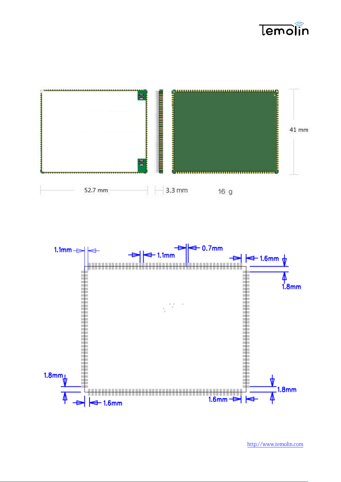
5 Mechanical Dimensions
Figure :Module Top and Side Dimensions
Figure : Layout PCB footprint example
Tel:+86-21-52242515 15 / 18

Device Installation and User Manual
5
The M100 module is a proprietary product designed and manufactured by Temolin Technologies Co.,
Ltd.. For integration into telematics control units manufactured by Temolin Technologies Co., Ltd, Inc.
for automotive OEMs.
The module is limited to installation ONLY in an integrated device design review by Temolin
Technologies Co., Ltd.
During design process of the integrated device, the module is soldered onto the pcb of the integrated
device.
The integrated device must provide RF connectors to external antennas or RF traces to connect the
M100 modules to antennas inside the integrated device.
The typical reference design for the trace layout, including PCB stack-up and trace length is as described
and shown in a Figure 3 below:
Typical RF trace layout between the M100 module and RF Connector for WIFI/BT/GPS antenna:
- Recommended RF Coonnector Type: Fakra
- Recommended RF trace length is less than 50 mm and width less than 2mm.
- WIFI/BT/GPS antenna connector is J1004.
Fig. 3. Typical trace routing recommended for use with the M100 module
Tel:+86-21-52242515 16 / 18

- PCB Material: FR 4
- PCB design information:
- Microstrip on layer 1 with ground on layer 2 / 50 ohm Single Endded Line
Fig. 4. Recommended PCB stack-up information for use while integrating M100 module.
Antenna information (only below approved antennas can be used with modular) :
Type Model
manufacture
Shenzhen SWARD
WCDMA/CDMA/LTE
GAM/
antenna
SG1106Z-1R23B-100-A
Communication
Technology Co.,
Ltd
Shenzhen SWARD
LTE Diversity
antenna
SG1106Z-1R23B-100-A
Communication
Technology Co.,
Ltd
Shenzhen SWARD
WIFI/BT/GPS antenna
SS901S-6D10G-130-A
Communication
Technology Co.,
Ltd
Tel:+86-21-52242515 17 / 18

FCC Statement
This device complies with Part 15 of the FCC rules. Operation is subject to the
following two conditions: 1) this device may not cause harmful interference, and 2)
this device must accept any interference received, including interference that may
cause undesired operation.
Note: This equipment has been tested and found to comply with the limits for a Class
B digital device, pursuant to part 15 of the FCC Rules. These limits are designed to
provide reasonable protection against harmful interference in a residential installation.
This equipment generates uses and can radiate radio frequency energy and, if not
installed and used in accordance with the instructions, may cause harmful
interference to radio communications. However, there is no guarantee that
interference will not occur in particular installation. If this equipment does cause
harmful interference to radio or television reception, which can be determined by
turning the equipment off and on, the user is encouraged to try to correct the
interference by one or more of the following measures:
--Reorient or relocate the receiving antenna.
--Increase the separation between the equipment and receiver.
--Connect the equipment into an outlet on a circuit different from that to which the
--Consult the dealer or an experienced radio/TV technician for help.
Changes or modifications not expressly approved by the party responsible for
compliance could void the user’s authority to operate the equipment.
FCC Radiation Exposure Statement
This modular complies with FCC RF radiation exposure limits set forth for an
uncontrolled environment. This transmitter must not be co-located or operating in
conjunction with any other antenna or transmitter.
This device must operate with a minimum distance of 20 cm between the radiator
and user body.
receiver is connected.
Attention: Limited Single Modular Approval - this RF Module may not be sold to the generic public and
requires professional installation. Due to the fact that this RF Module is equipped with an
own shielding, the end-product incl. this RF Module has to show compliance to the FCC rules
(15C / radiated emissions).
(OEM) Integrator has to assure compliance of the entire end-product incl. the integrated RF
Module. Additional measurements (15C) and/or equipment authorizations
(e.g either a complete new certification or a Class II Permissive Change) may need to be
addressed depending on co-location or simultaneous transmission issues if applicable.
Integrator is reminded to assure that these installation instructions will not be made available to
the end-user of the final host device.
The Integrator will be responsible to satisfy SAR/ RF Exposure requirements, when the module
integrated into any (portable, mobile, fixed) host device.
The final host device, into which this RF Module is integrated" has to be labeled with an auxiliary
label stating the FCC ID of the RF Module, such as "Contains FCC ID: 2AM5I-TML-M100".
Tel:+86-21-52242515 18 / 18
 Loading...