

TEMIC U893BSE-FP, U893BSE, U893BSE-SP Datasheet
U893BSE
1.3 GHz Prescaler for PLL’s in TV, CATV and SAT TV Tuners
Technology: Bipolar
Features
D
D
Extrem low current consumption (typ. 18 mA)
D
Output harmonics strongly reduced
D
3 scaling factors 64/128/256 programmable at Pin 5
D
High input sensitivity
Case
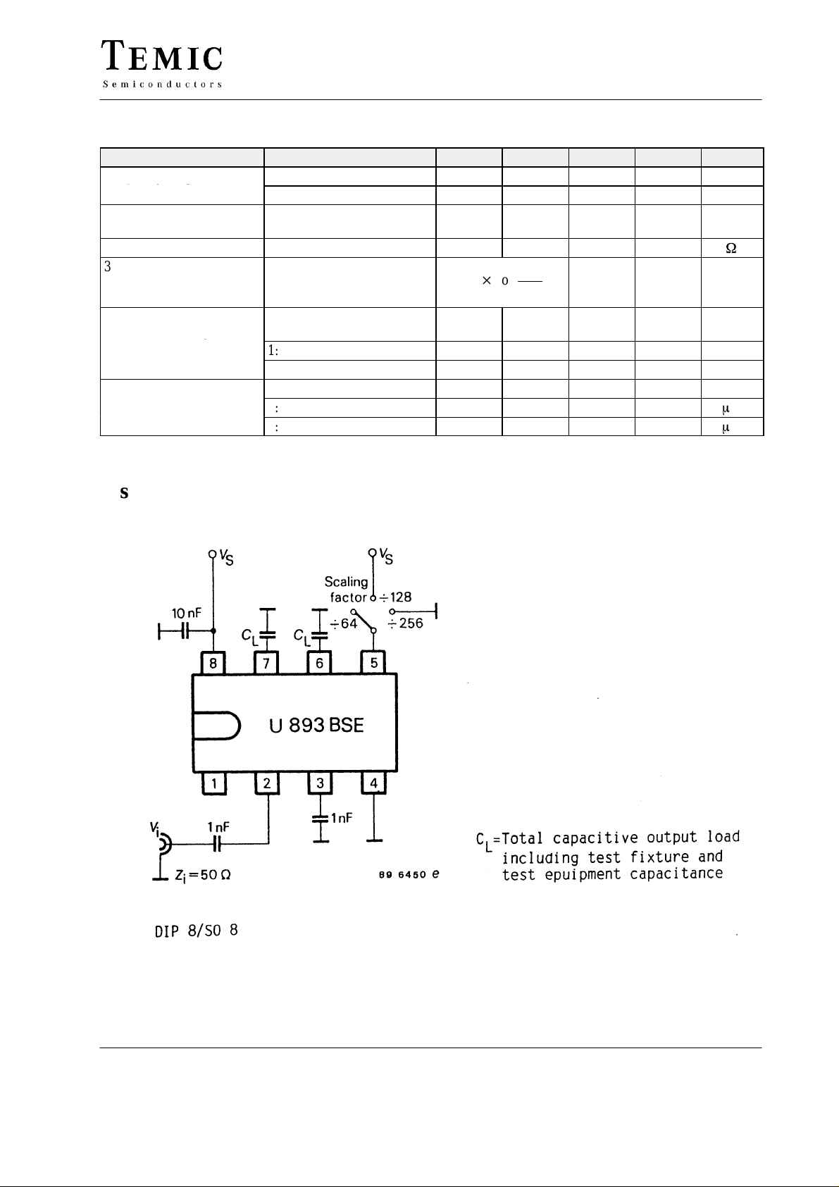
8 pin dual inline plastic (U893BSE)
8 pin SO plastic (U893BSE-FP)
6 pin SIP plastic (U893BSE-SP)
Emitter follower output stage
D
Electrostatic protection according to MIL–STD. 883
D
Pin compatible to U833BSE
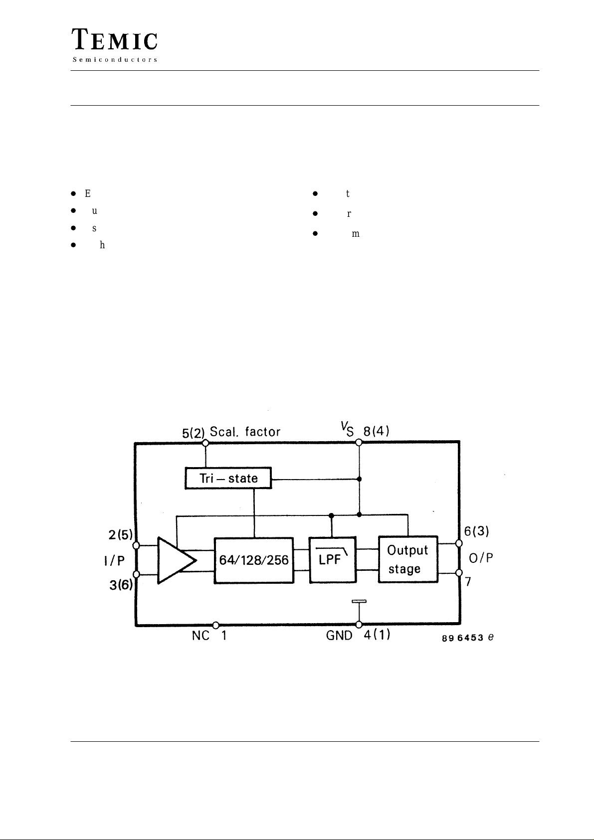
Block Diagram
TELEFUNKEN Semiconductors
Rev . A1, 23-Aug-96
1 (7)
U893BSE
Pin Configuration
Pin Function (DIP8, SO8)
1 n.c.
2, 3 Input
4 Ground
5 Switch 64/128/256
6, 7 Output
8 V
S
Pin Function (SIP6)
1 Ground
2 Switch 64/128/256
3 Output
4 V
5, 6 Input
Absolute Maximum Ratings
Reference point Pin 4 (1), unless otherwise specified
Parameters Symbol Value Unit
Supply voltage Pin 8 (4) V
Input voltage range Pin 2, 3, 5 (2, 5, 6) V
Junction temperature T
Ambient temperature range T
Storage temperature range T
Thermal Resistance
Parameters Symbol Maximum Unit
Junction ambient DIP8 R
SIP6 R
SO8 R
S
i
j
amb
stg
thJA
thJA
thJA
S
6 V
0 to V
S
V
125 °C
–25 to +85 °C
–40 to +125 °C
100 K/W
100 K/W
175 K/W
Electrical Characteristics
V
= 4.5 to 5.5 V, T
S
Parameters Test Conditions / Pin Symbol Min. Typ. Max. Unit
Supply voltage range Pin 8 (4) V
Supply current VS = 5 V Pin 8 (4) I
Input sensitivity
Large signal compatibility RG = 50
1)
RMS-voltage calculated from the measured available power
2 (7)
= 0 to 70 °C, referred to test circuit, unless otherwise specified
amb
1)
RG = 50
f
i
W
= 70 to 1100 MHz
Pin 2, 3 (5,
6)
fi = 1100 to 1200 MHz
Pin 2, 3 (5,
6)
fi = 1200 to 1300 MHz
Pin 2, 3 (5,
6)
W
Pin 2, 3 (5,
6)
S
S
v
i
v
i
v
i
V
i
4.5 5.5 V
21 25 mA
10 mV
15 mV
20 mV
300 mV
TELEFUNKEN Semiconductors
Rev . A1, 23-Aug-96
Parameters Test Conditions / Pin Symbol Min Typ Max Unit
qyg
g()
g
Frequency range f
f
Emitter follower output
Voltage swing each output
fi ≤ 1000 MHz, CL = 13 pF,
SF = 1:64 Pin 6, 7 (3)
Output impedance Pin 6, 7 (3) Z
3rd order harmonics
suppression
fi = 700 to 900 MHz,
C
= 13 pF, SF = 1:64
L
Pin 6, 7 (3)
Switching voltage for
scaling factor (SF)
1:64 Pin 5 (2) V
1:128 V
1:256 V
Switching current V
= 5 V Pin 5 (2)
S
1:128 VSF = 5 V I
1:256 VSF = 0 V I
imin
imax
V
O
O
20 log
SF
SF
SF
SF
SF
U893BSE
70 MHz
1300 MHz
0.6 0.7 V
200
V
O3f
V
O1f
VS – 0.5 V
–30 dB
open
0 0.3 V
150
–150
m
m
pp
W
A
A
Test Circuits
TELEFUNKEN Semiconductors
Rev . A1, 23-Aug-96
3 (7)
 Loading...