

TEMIC U813BSE-FP, U813BSE-SP, U813BSE, U813BS-SP, U813BS Datasheet
...
U813BS/U813BSE
1.1-GHz Prescaler for PLLs in TV, CATV and SAT TV Tuners
Technology: Bipolar
Features
D
D
U813BS ECL output stage
D
U813BSE emitter-follower output stage
D
3 scaling factors 64/128/256, programmable at Pin 5
D
High input sensitivity
Case
8-pin dual-inline plastic (U813BS, U813BSE)
8-pin SO plastic (U813BS-FP, U813BSE-FP)
6-pin SIP plastic (U813BS-SP, U813BSE-SP)
Low output impedance
D
Low power consumption
D
Pin-compatible to the U6xxB-series except Pin 5
D
Electrostatic protection according to MIL-STD. 883
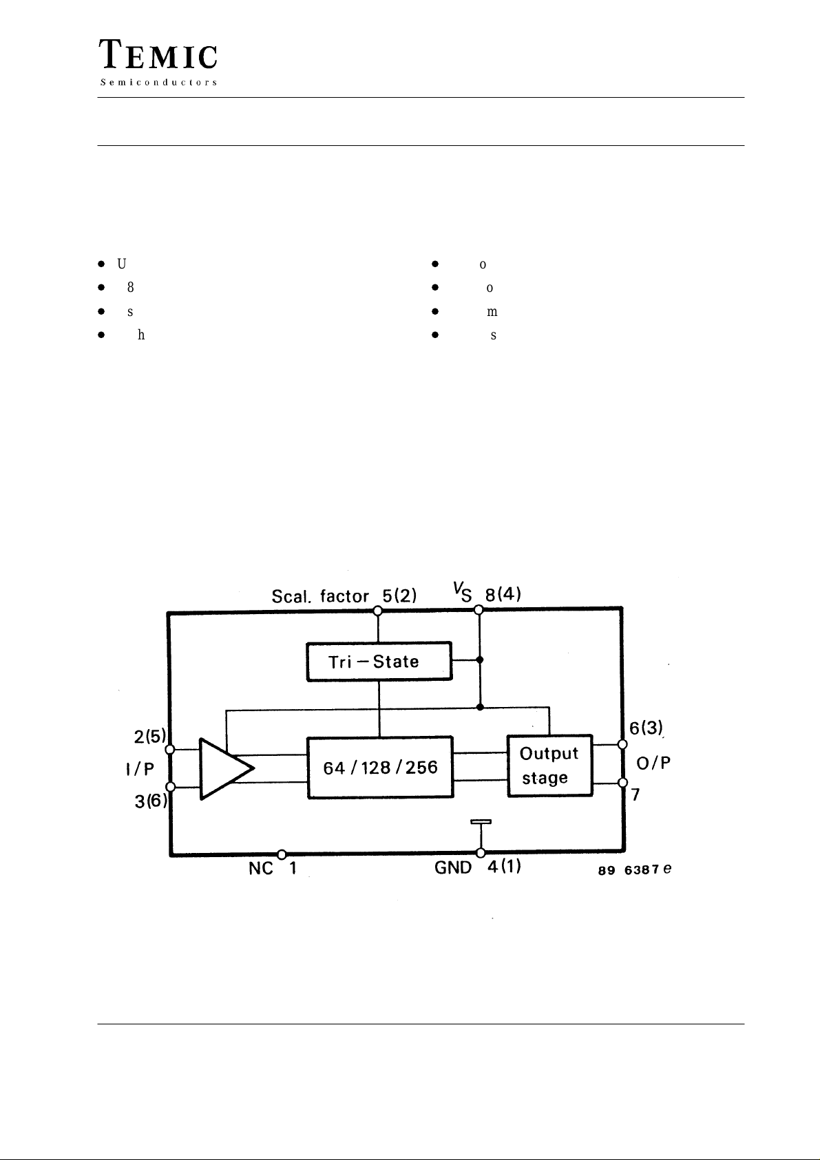
Block Diagram
Figure 1. Block diagram
TELEFUNKEN Semiconductors
Rev . A1, 05-Sep-96
1 (7)
U813BS/U813BSE
Absolute Maximum Ratings
Reference point pin 4 (1)
Parameters Symbol Value Unit
Supply voltage Pin 8 (4) V
Input-voltage range Pin 2, 3, 5 (2, 5, 6) V
Junction temperature T
Storage-temperature range T
Ambient-temperature range T
Thermal Resistance
Parameters Symbol Value Unit
Junction ambient DIP8 100
SIP6
SO8 175
Note:
The device is self-oscillating without input signal
R
S
i
i
stg
amb
thJA
0 to V
125 °C
–40 to +125 °C
–25 to +70 °C
100
6 V
S
K/W
V
Pin Description (Dip8, SO8)
Pin Function
1 Not connected
2, 3 Input
4 Ground
5 Switch 64/128/256
6, 7 Output
8 V
Notes:
Pin numbers without brackets apply to DIP8 and SO8 package,
Pin numbers with brackets to SIP6
RMS voltage calculated from the available power measured
S
Pin Description (SIP6)
Pin Function
1 Ground
2 Switch 64/128/256
3 Output
4 V
5,6 Input
S
2 (7)
TELEFUNKEN Semiconductors
Rev . A1, 05-Sep-96
Electrical Characteristics
qyg
imin
MH
gg
U813BS/U813BSE
VS = 4.5 to 5.5 V, T
= 0 to +70_C, referred to test circuit, unless otherwise specified
amb
Parameters Test Conditions / Pin Symbol Min. Typ. Max. Unit
Supply current VS = 5 V
U813BS Pin 8 (4)
U813BSE Pin 8 (4) I
Input sensitivity RG = 50
f
i
W
= 70 to 1000 MHz
Pin 2, 3 (5, 6)
f
= 1000 to 1100 MHz
i
Pin 2, 3 (5, 6)
Large-signal compatibility RG = 50
W
Pin 2, 3 (5, 6)
Frequency range f
Output stage
a. Balanced ECL output
Voltage swing each
output
RL = 10 k//13 pF
Pin 6, 7 (3)
Output impedance Pin 6, 7 (3) Z
b. Emitter follower
Voltage swing each
output
RL = 10 k//13 pF
Pin 6, 7 (3)
Output impedance Pin 6, 7 (3) Z
Switching voltage for ./. 64 Pin 5 (2) V
./. 128 Pin 5 (2) V
./. 256 Pin 5 (2) V
imin
f
imax
V
V
I
S
S
V
i
V
i
V
i
300 mV
35 45 mA
38 50 mA
10 mV
15 mV
70
z
1100
O
O
O
O
SF
SF
SF
0.8 V
500
1 V
200
open
VS –0.5 V
0 0.5 V
pp
W
pp
W
TELEFUNKEN Semiconductors
Rev . A1, 05-Sep-96
3 (7)
 Loading...