

TEMIC U4280BM-BFL, U4280BM-B Datasheet
AM / FM - PLL
Description
The U4280BM is an integrated circuit in BICMOS
technology for frequency synthesizer. It performs all the
functions of a PLL radio tuning system and is controlled
Features
D
Frequency range up to 150 MHz
D
Pre-amplifier for AM and FM
D
Fine tuning steps: AM y 1kHz
FM y 2 kHz
D
Two programmable 16-bit divider,
adjustable from 2 to 65535
Ordering Information
U4280BM
2
C bus. The device is designed for all frequency
by I
synthesizer applications of radio receivers, as well as
RDS (Radio Data System) applications.
D
Reference oscillator up to 15 MHz
D
5 programmable switching outputs,
4 are open drain outputs up to 15 V
D
Phase detector with separate outputs for AM and FM
2
D
Controlled via I
C bus
Extended Type Number Package Remarks
U4280BM-B DIP20
U4280BM-BFL SO20
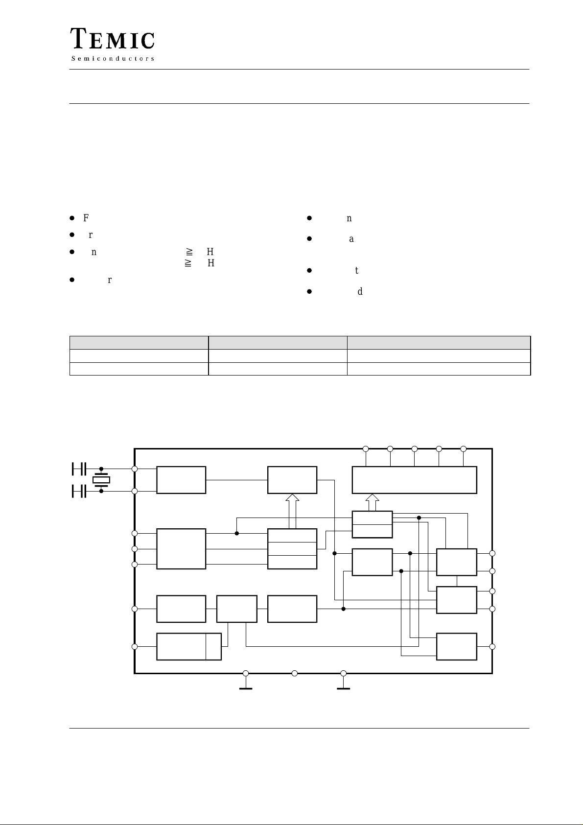
Block Diagram
PRT SWO1 SWO2 SWO3 AM/FM
OSCIN
OSCOUT
SCL
SDA
AS
AMOSC
18
19
2
3
4
12
Oscillator
I2C – BUS
interface
Preamplifier
AM / FM–
switch
R – Divider Switching outputs
Latch
Shift register
Latch
N – Divider
5 6789
Latch
Status
Phase
detector
Current
sources
Analog
outputs
14
15
13
16
PDFM
PDAM
PDFMO
PDAMO
10
FMOSC
Preamplifier : 2
TELEFUNKEN Semiconductors
Rev . A1, 10-Apr-97
11
GND2
Figure 1. Block diagram
1
V
DD
20
GND1
Preliminary Information
Lock
detector
17
13346
LD
1 (9)
U4280BM
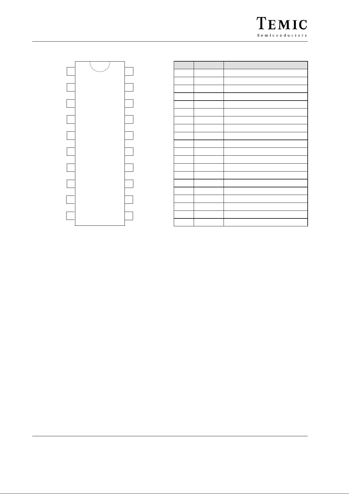
Pin Description
V
DD
SCL
SDA
AS
PRT
SWO1
SWO2
SWO3
AM/FM
FMOSC
1
2
3
4
5
6
7
8
9
10
Figure 2. Pinning
13319
20
19
18
17
16
15
14
13
12
11
GND
1
OSCOUT
OSCIN
LD
PDAMO
PDAM
PDFM
PDFMO
AMOSC
GND
Pin Symbol Function
1 V
2 SCL I2C bus clock
3 SDA I2C bus data
4 AS Address selection
5 PRT Switching port
6 SWO1 Switching output 1
7 SWO2 Switching output 2
8 SWO3 Switching output 3
9 AM/FM Switching output AM/FM
10 FMOSC FM oscillator input
11 GND2 Ground 2 (analog)
12 AMOSC AM oscillator input
13 PDFMO FM analog output
14 PDFM FM current output
15 PDAM AM current output
16 PDAMO AM analog output
17 LD Lock detect
18 OSCIN Oscillator input
19 OSCOUT Oscillator output
20 GND1 Ground 1 (digital)
DD
Supply voltage
Functional Description
The U4280BM is controlled via the 2-wire I2C bus. For
programming there are one module address byte, two
subaddress bytes and five data bytes.
The module address contains a programmable address bit
A 1 which with address select input AS (Pin 4) makes it
possible to operate two U4280BM-B in one system. If bit
A 1 is identical with the status of the address select input
AS, the chip is selected.
The subaddress determines which one of the data bytes is
transmitted first. If subaddress of R-divider is
transmitted, the sequence of the next data bytes is DB 0
(Status), DB 1 and DB 2.
If subaddress of N-divider is transmitted, the sequence of
the next data bytes is DB 3 and DB 4. The bit organisation
of the module address, subaddress and 5 data bytes are
shown in figure 2
2 (9)
Preliminary Information
2
Each transmission on the I
“START”-condition and has to be ended by the “STOP”condition (see figure 3).
The integrated circuit U 4283 BM has two separate inputs
for AM and FM oscillator. Pre-amplified AM signal is
directed to the 16 bit N-divider via AM/FM switch,
whereas (pre-amplified) FM signal is first divided by a
fixed prescaler (:2). AM/FM switch is controlled by
software. Tuning steps can be selected by 16 bit
R-divider. Further there is a digital memory phase
detector. There are two separate current sources for AM
and FM amplifier (charge pump) as given in electrical
characteristics. It allows independent adjustment of gain,
whereby providing high current for high speed tuning and
low current for stable tuning.
TELEFUNKEN Semiconductors
C bus begins with the
Rev . A1, 10-Apr-97
U4280BM
Bit Organization
MSB LSB
Module address 1 1 0 0 1 0 0/1 0
A7 A6 A5 A4 A3 A2 A1 A0
Subaddress (R-divider) X X X X 0 1 X X
Subaddress (N-divider) X X X X 1 1 X X
MSB LSB
Data byte 0 (Status) PRT SWO1 SWO2 SWO3 AM/
FM
D7 D6 D5 D4 D3 D2 D1 D0
PD
ANA
PD
POL
PD
CUR
Data byte 1 2
Data byte 2 2
Data byte 3 2
Data byte 4 2
AM/FM FM-operation AM-operation
PD - ANA PD analog TEST
PD - POL Negative polarity Positive polarity
PD - CUR Output current 2 Output current 1
15
15
R-divider 2
7
7
LOW HIGH
Figure 3.
R-divider 2
N-divider 2
N-divider 2
8
0
8
0
TELEFUNKEN Semiconductors
Rev . A1, 10-Apr-97
3 (9)
Preliminary Information
 Loading...