

查询U2090B供应商
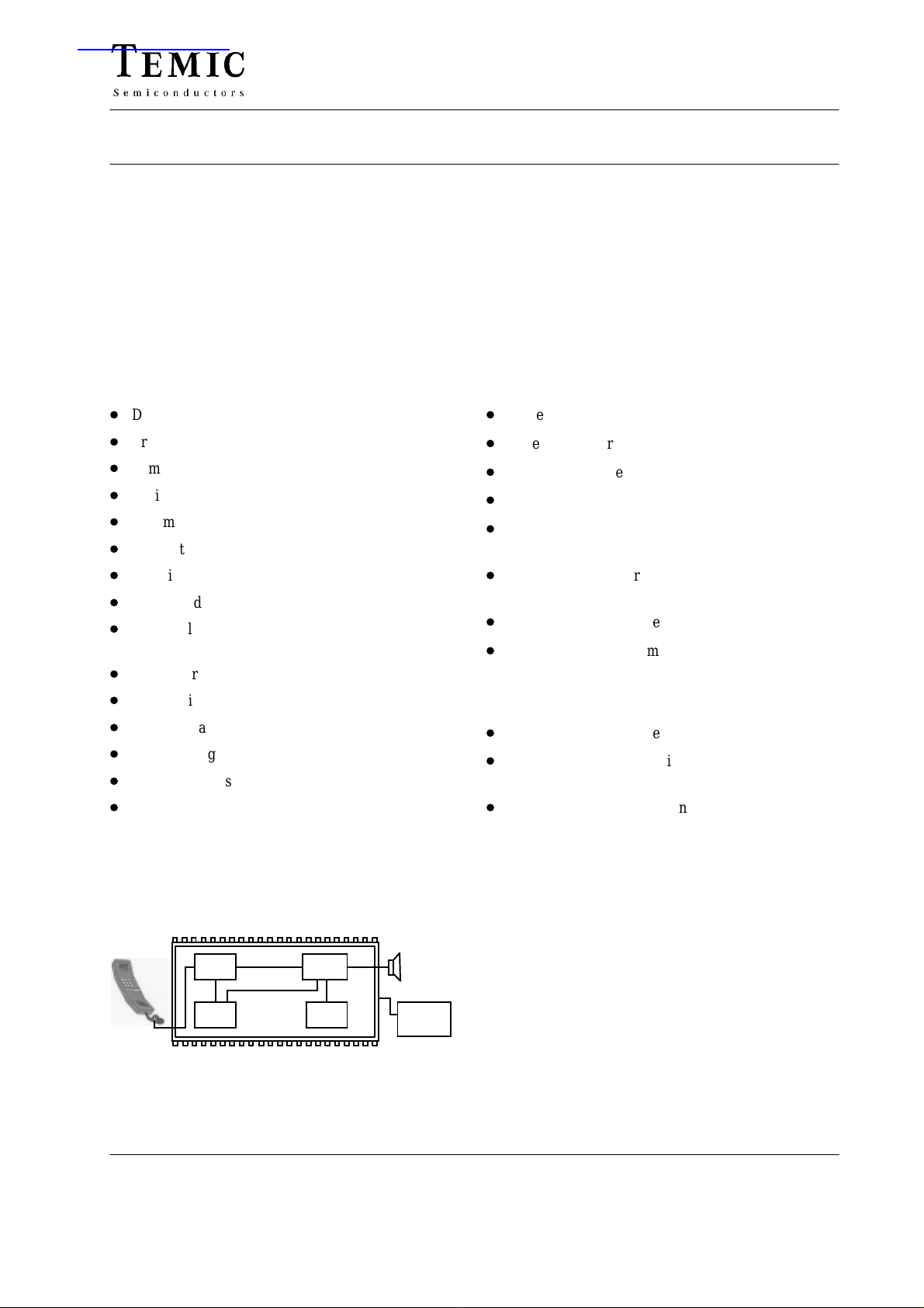
Monolithic Integrated Feature Phone Circuit
Description
The µc controlled telephone circuit U4090B is a linear
integrated circuit for use in feature phones, answering
machines and fax machines. It contains the speech circuit,
tone ringer interface with dc/dc converter, sidetone
equivalent and ear protection rectifiers. The circuit is line
powered and contains all components necessary for
amplification of signals and adaptation to the line.
Features
D
DC characteristic adjustable
D
Transmit and receive gain adjustable
D
Symmetrical input of microphone amplifier
D
Anti-clipping in transmit direction
D
Automatic line loss compensation
D
Symmetrical output of earpiece amplifier
An integrated voice switch with loudspeaker amplifier
allows loudhearing or handsfree operation. With an
anti-feedback function, acoustical feedback during
loudhearing can be reduced significantly. The generated
supply voltage is suitable for a wide range of peripheral
circuits.
D
Voice switch
D
Tone ringer interface with dc/dc converter
D
Zero crossing detection
D
Common speaker for loudhearing and tone ringer
D
Supply voltages for all functional blocks of a
subscriber set
U4090B
D
Built-in ear protection
D
DTMF and MUTE input
D
Adjustable sidetone suppression independent
of sending and receiving amplification
D
Speech circuit with two sidetone networks
D
Built-in line detection circuit
D
Integrated amplifier for loudhearing operation
D
Anti-clipping for loudspeaker amplifier
D
Improved acoustical feedback suppression
D
Power down
Applications
Feature phone, answering machine, fax machine, speaker
phone
Speech
circuit
Voice
switch
Audio
amplifier
Tone
ringer
Loudhearing
and
Tone ringing
MC with
EEPROM/
DTMF
D
Integrated transistor for short circuiting the line
voltage
D
Answering machine interface
D
Operation possible from 10 mA line currents
Benefits
D
Savings of one piezo electric transducer
D
Complete system integration of analog signal processing on one chip
D
Very few external components
TELEFUNKEN Semiconductors
Rev . C1, 28-Oct-96
94 8741
1 (34)
Preliminary Information
U4090B
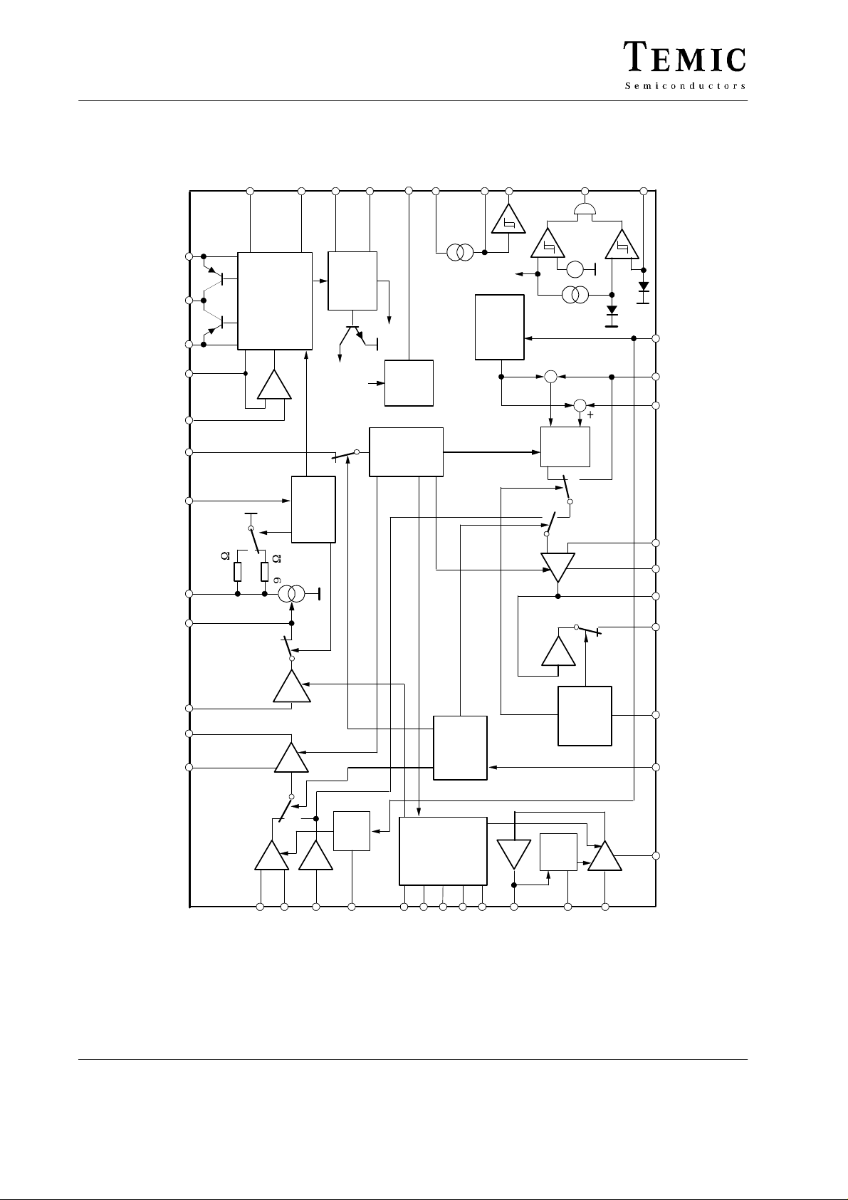
Block Diagram
MPS
V
MP
14 13
V
B
11
V
10
SENSE
7
IND
31
AGA
21
IMPSEL
L
8
33
W
600
M
V
34
Power
supply
W
900
GND
9
control
Impedance
6
L
V
Current
PD
Q
32
supply
S
L
I
I
REF
20
I Supply
Line
AGA
LIDET
17
detect
control
RING
V
16
OSC
C
15
MP
V
Receive
attenuation
SW
OUT
RA1
RFDO
19
–
+
–
+
–
+
ST
BAL
THA
18
–
+
43
RECIN
STIS
37
38
STIL
RAC
3941
GR
40
RECO1
GT MICOTXIN STO V
94 8064
RA2
–1
MIC
5
TXA
MIC1
4
DTMF
MIC2
2
DTMF
TX
TTXA
ACL
42
28
27
INLDR
INLDT
mute
Transmit
control
feedback
Acoustical
suppression
30
29
TLDT
TLDR
control
26
ATAFS
12
SA
SAO
Mute
SACL
22
TSACL
control
receive
SAI
24
SAI
44
3
1
36
RECO2
35
MUTR
25
MUTX
GSA
23
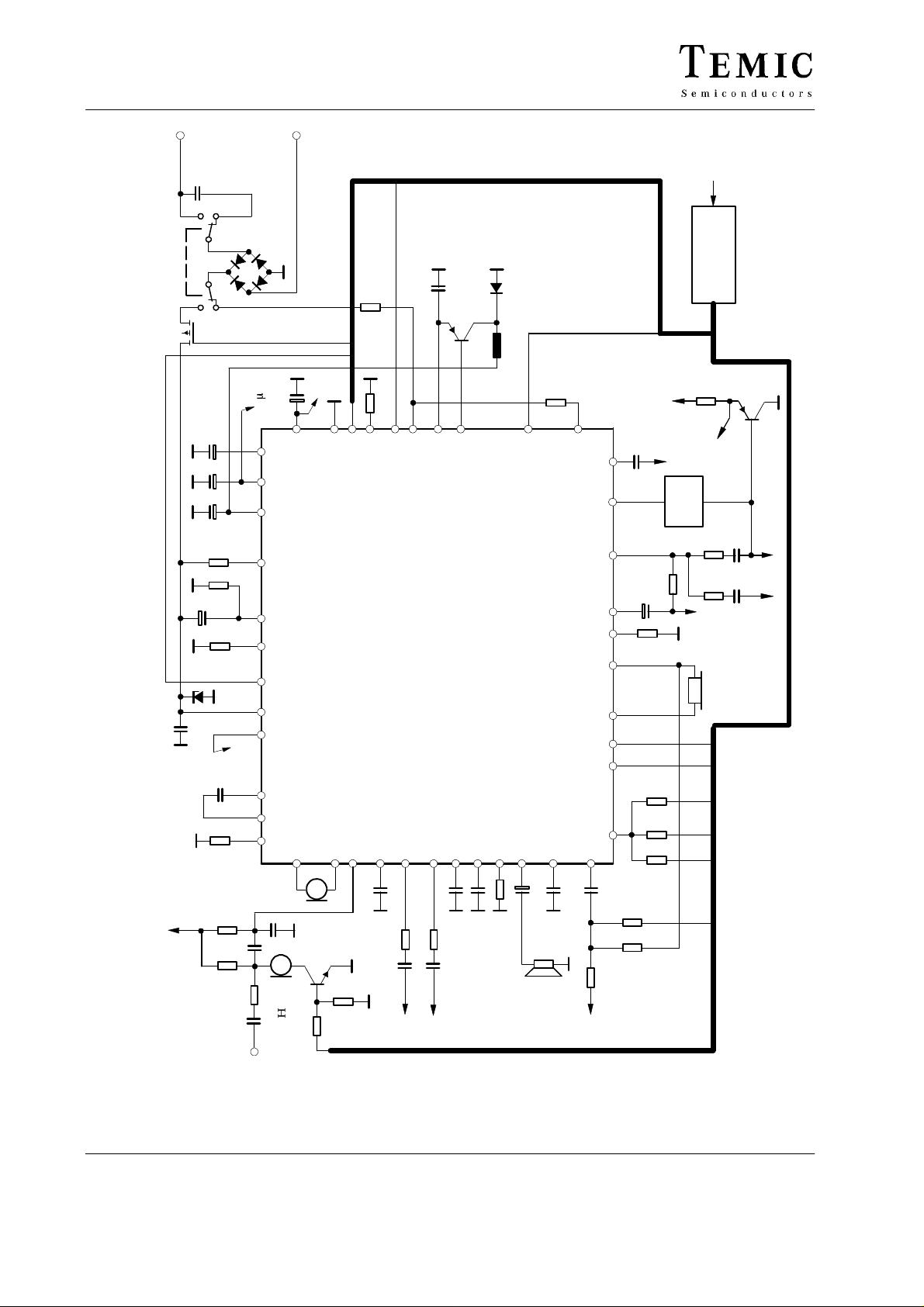
Figure 1.
2 (34)
TELEFUNKEN Semiconductors
Rev . C1, 28-Oct-96
Preliminary Information
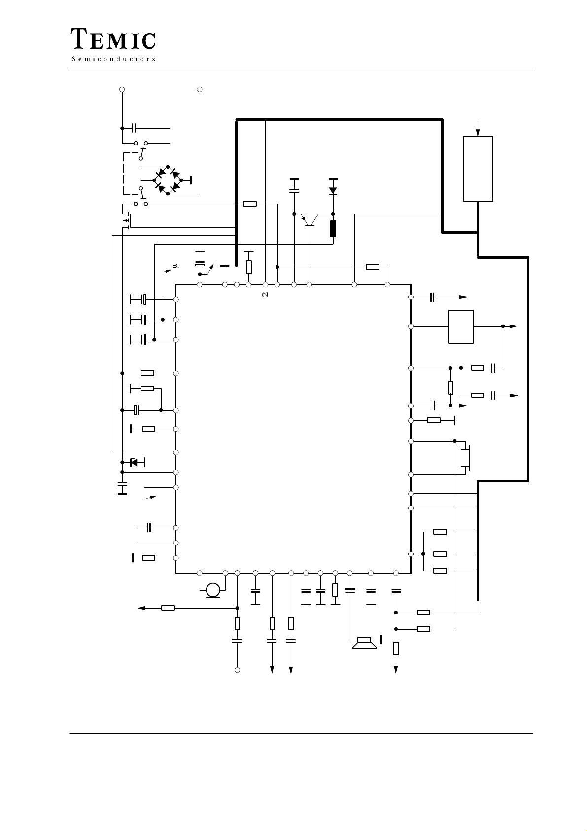
Tip
hook switch
U4090B
7
C
Ring
5
R
9
C
1
Q
1
L
MP
V
Micro
controller
19
12
16
C
speaker
R
22
7
10
38
39
40 41
36
35
25
23
C
R
13
C
11
R
R
R
14
C
17
R
14
R
15
R
16
R
18
43
37
24
15
C
M
V
10
12
13
L
V
STIN 2
(Option)
R
M
V
11
8
C
9
R
12
C
Earpeace
94 8849
STO
M
V
C
m
to C
6
5 C
C
4
C
4
R
3
R
3
C
2
R
13 V
2
C
1
C
1
R
M
V
to STIN
28
R
11 14 13
10
7
31
21
8
33
44
3
1
Micro–
phone
34
5
9
4
27
R
DTMF
Generator
6
R
6
32
20
17
16
15
U4090B
2
42
21
C
R
C
22
C
28
20
20
RECO
27
19
R
MICO
30
18
C
19
C
26
29
31
17
R
C
Loud-
M
8
V
TELEFUNKEN Semiconductors
Rev . C1, 28-Oct-96
Figure 2. Application circuit for loudhearing
3 (34)
Preliminary Information
U4090B
Tip
hook switch
M
V
Ring
7
C
5
R
M
V
8
m
C
to C
6
C
5
C
4
C
4
R
3
3
R
C
2
R
13 V
2
C
1
C
1
R
C
25
R
26
R
25
R
DTMF
to STIN
Micro–
24
C
11 14 13
10
21 31 7
8
33
44
3
1
phone
24
C
HF–Mic
23
9
34
5
4
23
R
6
R
6
20
32
2
22
R
28
42
21
C
30
R
27
C
RECO
17
29
R
9
C
1
Q
16
15
U4090B
27
30
17
18
C
C
26
C
LOGTX
1
L
7
R
19
29
26
12
18
R
16
C
Loud
22
15
C
speaker
18
43
37
38
41 39
40
36
35
25
23
24
14
C
17
R
M
V
B
V
10
C
10
R
13
C
11
R
12
R
13
R
14
R
15
R
16
R
L
V
STIN 2
(Option)
MP
V
Micro–
21
R
LOGTX
8
R
9
R
M
V
Earpiece
94 8850
controller
BC177
11
C
12
C
STN
M
V
4 (34)
Figure 3. Application for handsfree operation
TELEFUNKEN Semiconductors
Rev . C1, 28-Oct-96
Preliminary Information
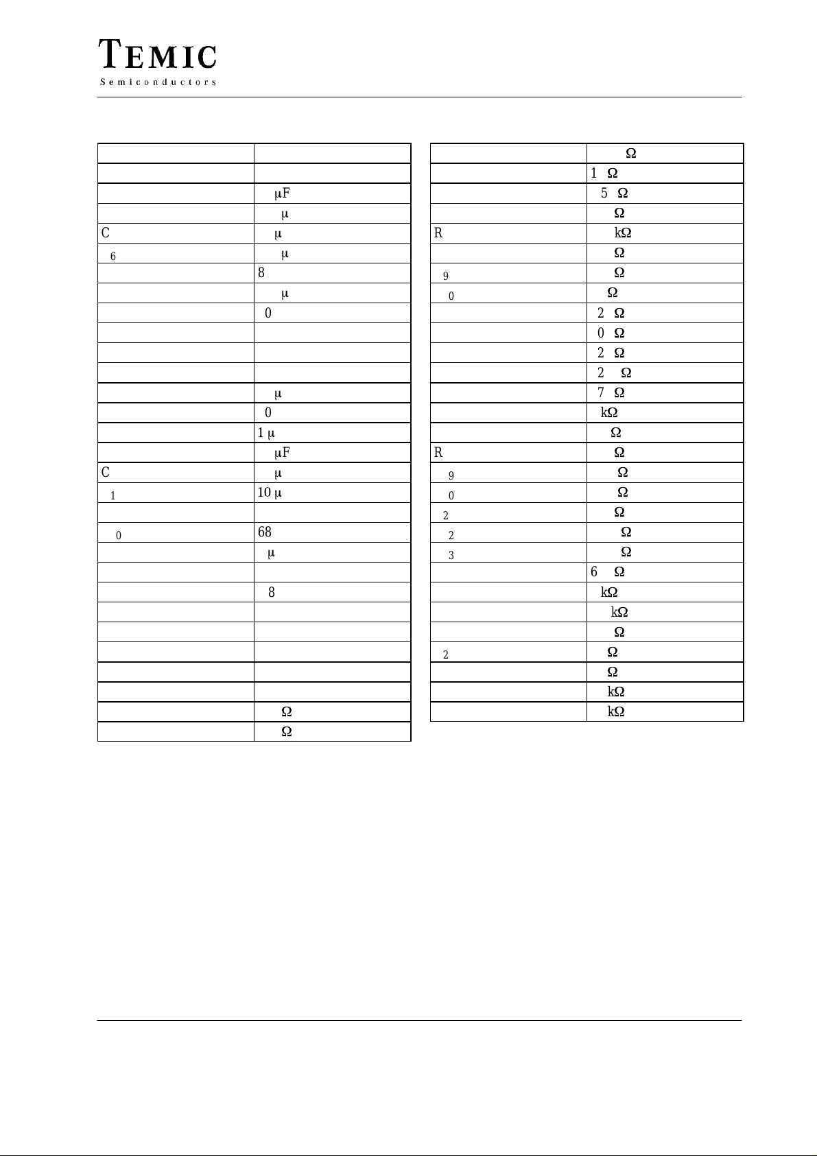
Typical value of external components
U4090B
C
1
C
2
C
3
C
4
C
5
C
6
C
7
C
8
C
9
C
10
C
11
C
12
C
13
C
14
C
15
C
16
C
17
C
18
C
19
C
20
C
21
C
22
C
23
C
24
C
25
C
26
C
27
L
1
R
1
R
2
100 nF
4.7 nF
10 mF
220 mF
47 mF
470 mF
820 nF
100 mF
100 nF
150 nF
68 nF
33 nF
10 mF
100 nF
1 m
F
47 mF
10 mF
10 m
F
68 nF
68 nF
1 mF
100 nF
6.8 nF
10 nF
100 nF
470 nF
33 nF
2.2 mH
27 k
W
20 k
W
R
3
R
4
R
5
R
6
R
7
R
8
R
9
R
10
R
11
R
12
R
13
R
14
R
15
R
16
R
17
R
18
R
19
R
20
R
21
R
22
R
23
R
24
R
25
R
26
R
27
R
28
R
29
R
30
R
31
> 68 k
10
W
1.5 k
62 k
W
680 k
22 k
W
330
W
3 k
W
62 k
W
30 k
W
62 k
W
120 k
47 k
W
1 k
W
1.2
W
30 k
W
6.8 k
6.8 k
15 k
W
330 k
220 k
68 k
W
2 k
W
3.3 k
18 k
W
2 k
W
1 k
W
12 k
W
56 k
W
W
W
W
W
W
W
W
W
W
TELEFUNKEN Semiconductors
Rev . C1, 28-Oct-96
5 (34)
Preliminary Information
U4090B
G
DTMF
MICO
MIC2
MIC1
PD
IND
V
GND
SENSE
V
SAO
V
MPS
V
MP
SWOUT
COSC
VRING
THA
RFDO
LIDET
IMPSEL
TSACL
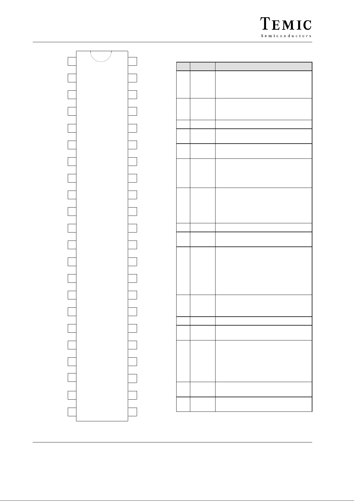
Pin Description
T
1
2
3
4
5
6
7
8
L
9
10
11
B
U4090B
12
13
14
15
16
17
18
19
20
21
22
44
43
42
41
40
39
38
37
36
35
34
33
32
31
30
29
28
27
26
25
24
23
TXIN
RECIN
TTXA
G
R
RECO1
RAC
STIL
STIS
RECO2
MUTR
V
M
STO
IREF
AGA
TLDR
TLDT
INLDR
INLDT
ATAFS
MUTX
SAI
GSA
Pin Symbol Function
1 G
2 DTMF Input for DTMF signals,
3 MICO Output of microphone preamplifier
4 MIC 2 Non-inverting input of microphone
5 MIC 1 Inverting input of microphone
6 PD Active high input for reducing the
7 IND The internal equivalent inductance of
8 V
9 GND Reference point for dc- and ac-output
10 SENSE A small resistor (fixed) connected
11 V
12 SAO Output of loudspeaker amplifier
13 V
14 V
SWOUT
15
16 COSC 40 kHz oscillator for ringing power
A resistor from this pin to GND sets the
T
amplification of microphone and DTMF
signals, the input amplifier can be muted
by applying VMP to G
also used for the answering machine
and handsfree input
amplifier
amplifier
current consumption of the circuit,
simultaneously V
internal switch
the circuit is proportional to the value
of the capacitor at this pin,
a resistor connected to ground may be
used to reduce the dc line voltage
Line voltage
L
signals
from this pin to V
the dc characteristic and also effects
the line length equalization
characteristics and the line current at
which the loudspeaker amplifier is
switched on
Unregulated supply voltage for
B
peripheral circuits (voice switch),
limited to typically 7 V
Unregulated supply voltage for µP,
MPS
limited to 6.3 V
Regulated supply voltage 3.3 V for
MP
peripheral circuits (especially
microprocessors),
minimum output current: 2 mA
(ringing)
4 mA (speech mode)
Output for driving external switching
transistor
converter
T
is shorted by an
L
sets the slope of
L
.
6 (34)
94 7905 e
TELEFUNKEN Semiconductors
Rev . C1, 28-Oct-96
Preliminary Information
U4090B
Pin Symbol Function
17 VRING Input for ringing signal protected by
internal zener diode
18 THA Threshold adjustment for ringing
frequency detector
19 RFDO Output of ringing frequency detector
20 LIDET Line detect; output is low when the
line current is more than 15 mA
21 IMP-
SEL
22 TSACL Time constant of anti-clipping of
23 GSA Current input for setting the gain of
24 SA I Speaker amplifier input (for
25 MUTX Three state input of transmit mute:
26 ATAFS Attenuation of acoustical feedback
27 INLDT Input of transmit level detector
28 INLDR Input of receive level detector
Control input for selection of line
impedance
1. 600 Ω
2. 900 Ω
3. Mute of second transmit stage
(TXA); also used for indication of
external supply (answering machine);
last chosen impedance is stored
speaker amplifier
the speaker amplifier,
adjustment characteristic is
logarithmical,
or RGSA > 2 MΩ, the speaker
amplifier is switched off
loudspeaker, tone ringer and
handsfree use)
1) Speech condition; inputs MIC1 /
MIC2 active
2) DTMF condition; input DTMF
active
a part of the input signal is
passed to the receiving amplifier
as a confidence signal during
dialing
3) Input DTMF used for answering
machine and handsfree use;
receive branch not affected
suppression,
maximum attenuation of AFS circuit
is set by a resistor at this pin,
without the resistor, AFS is switched
off
Pin Symbol Function
29 TLDT Time constant of transmit level
detector
30 TLDR Time constant of receive level
detector
31 AGA Automatic gain adjustment with line
current
a resistor connected from this pin to
GND sets the starting point
max. gain change: 6 dB.
32 IREF Internal reference current generation;
RREF = 62 kΩ; IREF = 20 µA
33 STO Side tone reduction output
output resistance is approx. 300 Ω,
maximum load impedance: 10 kΩ.
34 V
35 MUTR Three state mute input
36 RECO 2 Inverting output of receiving
37 STI S Input for side tone network (short
38 STI L Input for side tone network (long
39 RAC Input of receiving amplifier for ac
40 RECO 1 Output of receiving amplifier
41 G
42 TTXA Time constant of anticlipping in
43 RECIN Input of receiving path; input
44 TXIN Input of intermediate transmit stage,
Reference node for microphone-
M
earphone and loudspeaker amplifier,
supply for electret microphone
(IM ≤ 700 mA)
1. Normal operation
2. Mute of ear piece
3. Mute of RECIN signal
Condition of earpiece mute is stored
amplifier
loop) or for answering machine
loop)
coupling in feedback path
A resistor connected from this pin to
R
GND sets the receiving amplification
of the circuit; amplifier RA1 can be
muted by applying VMP to GR
transmit path
impedance is typically 80 k
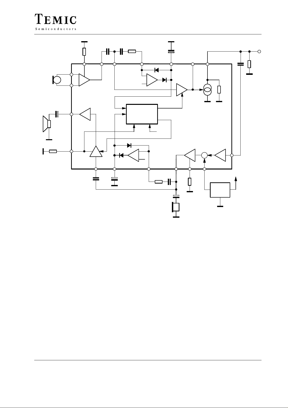
input resistance is typically 20 kΩ
W
TELEFUNKEN Semiconductors
Rev . C1, 28-Oct-96
7 (34)
Preliminary Information
U4090B
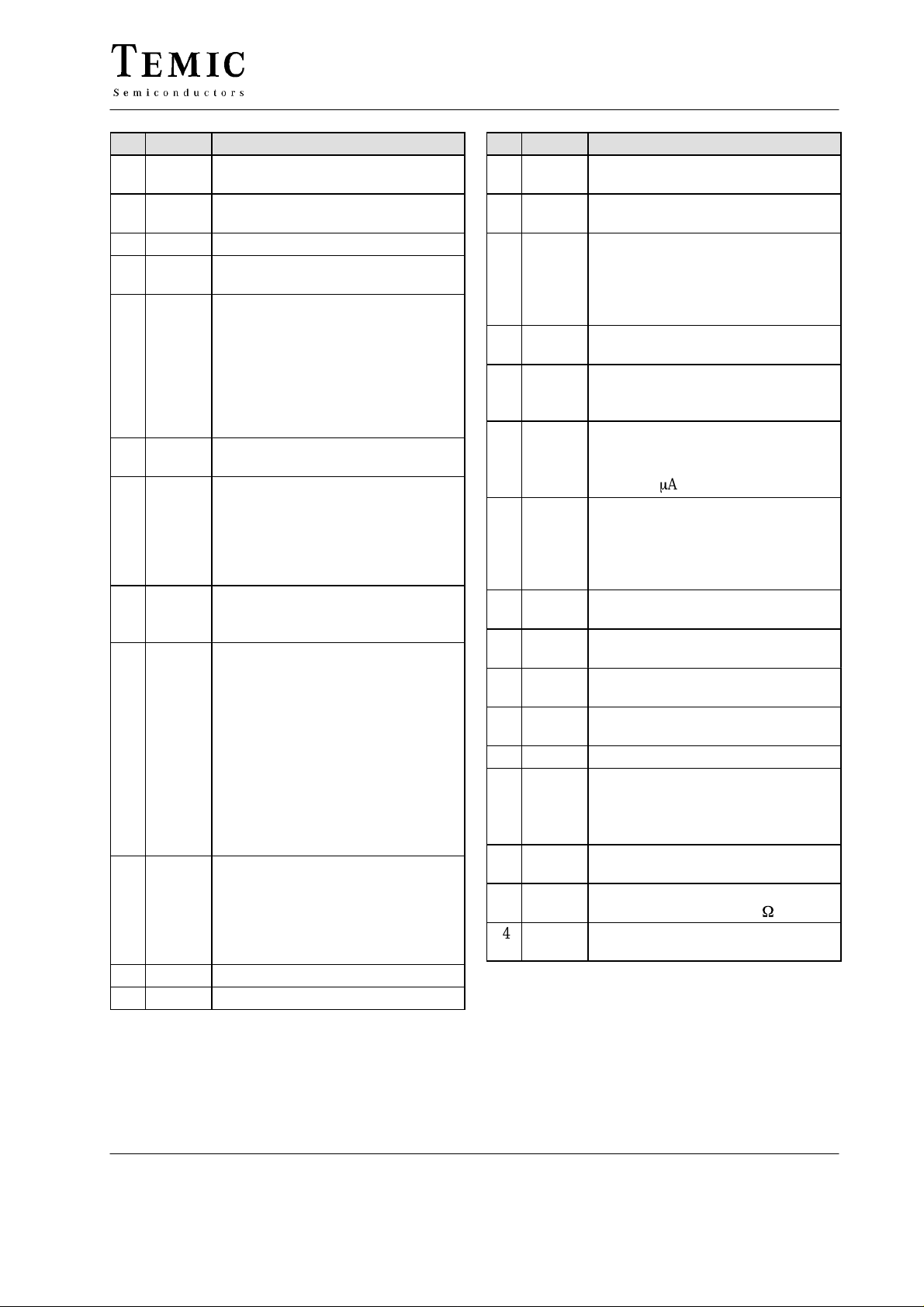
DC line interface and supply voltage generation
The DC line interface consists of an electronic inductance
and a dual port output stage, which charges the capacitors
at V
and VB. The value of the equivalent inductance
MPS
is given by
L = R
SENSE
@ C
@ (RDC @ R30) / (R
IND
+ R30)In
DC
order to improve the supply during worst case operating
conditions two PNP current sources - I
V
L
10
W
SENSE
BOPT
and
I
MPSOPT
voltages, when the NPNs in parallel are unable to conduct
current.
A flowchart for the control of the current sources
(figure 5) shows, how a priority for supply V
achieved.
- hand an extra amount of current to the supply
MPS
is
R
SENSE
C
IND
m
10 F
IND
R
DC
Figure 4. DC line interface with electronic inductance and generation of a regulated and an unregulated supply
I
< 5 mA
=
94 8047
VMPS < 6.3 V
BOPT
+
–
30 k
R
30
V
W
OFFS
Y
VSENSE–VMPS>200 mV
N
N
–
+
+
–
I
MPSOPT
< 5 mA
=
3.3 V
7.0 V
6.3 V
V
MPS
V
MP
3.3 V/
2 mA
V
B
470 F
m
47 F
m
220 F
m
8 (34)
Y
Charge CMPS
(IMPSOPT)
94 8058
Figure 5. Supply capacitors CMPS and CB are charged with priority on CMPS
VSENSE–VB>200 mV
Y
VB < 6.3 V
Y
Charge CB
(IBOPT)
N
N
IMPSOPT = 0
IBOPT = 0
Reduce IBOPT
(IMPSOPT = 0)
TELEFUNKEN Semiconductors
Preliminary Information
Rev . C1, 28-Oct-96
U4090B
The U4090B contains two identical series regulators,
which provide a supply voltage V
of 3.3 V suitable for
MP
a microprocessor. In speech mode both regulators are
active, because V
and VB are charged simultaneously
MPS
by the DC-line interface. Output current is 4 mA. The
capacitor at V
is used to provide the microcomputer
MPS
with sufficient power during long line interruptions. Thus
long flash pulses can be bridged or a LCD display can be
turned on for more than 2 seconds after going on hook.
When the system is in ringing mode, V
is charged by the
B
on chip ringing power converter. In this mode only one
regulator is used to supply V
V
RING
V
L
QS
with max. 2 mA.
MP
RPC
Power
supply
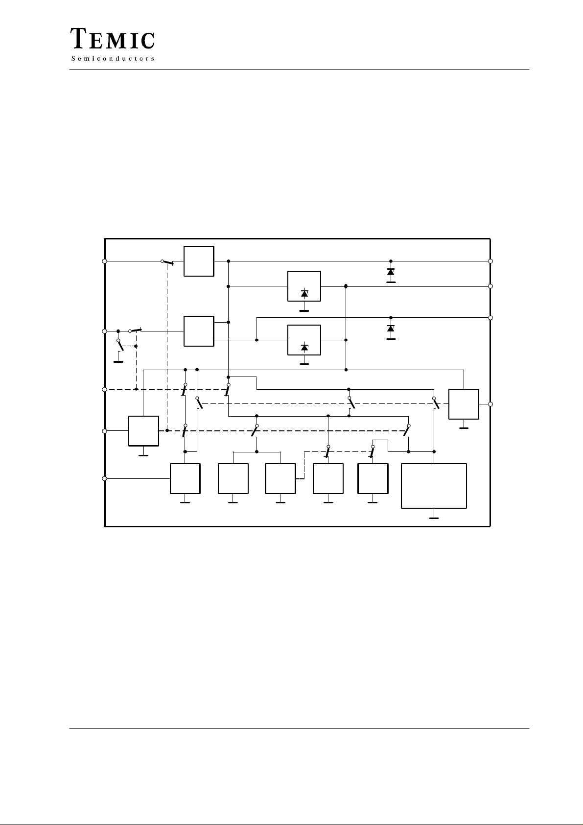
Supply structure of the chip
As a major benefit the chip uses a very flexible system
structure, which allows simple realization of numerous
applications such as:
group listening phone
handsfree phone
ringing with the built in speaker amplifier
answering machine with external supply
The special supply topology for the various functional
blocks is illustrated in figure 6.
Voltage
regulator
Voltage
regulator
7 V
6.3 V
V
V
V
B
MP
MPS
PD
LIDET
RFDO
LIDET
V
Lon
RFD
Figure 6. Supply of functional blocks is controlled by input voltages VL, VB, V
TXA
TXACL
and by logic inputs PD and IMPSEL
OFFSA
COMP
There are four major supply states:
1. Speech condition
2. Power down (pulse dialing)
3. Ringing
4. External supply
1. In speech condition the system is supplied by the line
current. If the LIDET-block detects a line voltage
above the fixed threshold (1.9 V), the internal signal
VLON is activated, thus switching off RFD and RPC
and switching on all other blocks of the chip.
ES
SAI,SA
SACL
AFS
IMPED
CONTR
MIC, DTMF
AGA, RA1, RA2
TX MUTE
MUT REC, STBAL
RECATT
ring
IMPSEL
94 8046
For line voltages below 1.9 V the switches remain in their
quiescent state as shown the diagram.
OFFSACOMP disables the group listening feature (SAI,
SA, SACL, AFS) below line currents of approximately
10 mA.
2. When the chip is put into Power-down mode
(PD = high), e.g. during pulse dialing, the internal
switch QS shorts the line and all amplifiers are
switched off. In this condition LIDET, voltage
regulators and IMPED CONTR are the only active
blocks.
TELEFUNKEN Semiconductors
Rev . C1, 28-Oct-96
9 (34)
Preliminary Information
U4090B
3. During ringing the supply for the system is fed into V
via the ringing power converter (RPC). The only
functional amplifiers are found in the speaker
amplifier section (SAI, SA, SACL).
4. In an answering machine the chip is powered by an
external supply via pin V
a posibility to activate all amplifiers (except the
transmit line interface TXA). Selecting IMP-
. This application demands
B
Handset
microphone
Log
B
SEL = high impedance activates all switches at the ES
line.
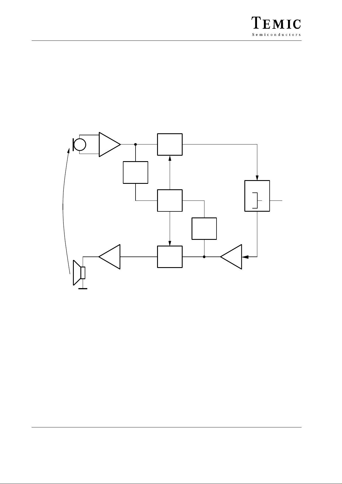
Acoustic feedback suppression
Acoustical feedback from the loudspeaker to the handset
microphone may cause instability in the system. The
U4090B offers a very efficient feedback suppression
circuit, which uses a modified voice switch topology.
figure 8 shows the basic system configuration.
TX
Att
Hybrid
Att
contr
Line
Loudspeaker
Figure 5. Basic voice switch system
Two attenuators (TX ATT and RX ATT) reduce the
critical loop gain by introducing an externally adjustable
amount of loss either in the transmit or in the receive
path.The sliding control in block ATT CONTR
determines, wether the TX or the RX signal has to be
attenuated. The overall loop gain remains constant under
all operating conditions.
Selection of the active channel is made by comparison of
Log
RX
Att
94 8956
the logarithmically compressed TX- and RX- envelope
curve.
The system configuration for group listening, which is
realized in the U 4090 B, is illustrated in figure 9. TXA
and SAI represent the two attenuators, whereas the
logarithmic envelope detectors are shown in a simplified
way (operational amplifiers with two diodes).
10 (34)
TELEFUNKEN Semiconductors
Rev . C1, 28-Oct-96
Preliminary Information
U4090B
VL
94 8059
SAO
GSA
GT MICO TIN INLDT TLDT
–
VBG
+
AFS
control
Max
att.
–
VBG
SAI
TLDR RECO1
SAI
+
INLDR
AGA
STO VL
TXA
GR
STIS
STN
Zint
RECIN
STO
Z
L
Figure 6. Integration of acoustic feedback suppression circuit into the speech circuit environment
A detailed diagram of the AFS (acountic feedback
suppression) is given in figure 10. Receive and Transmit
signals are first processed by logorithmic rectifiers in
TELEFUNKEN Semiconductors
Rev . C1, 28-Oct-96
Preliminary Information
order to produce the envelopes of the speech at TLDT and
RLDT. After amplification a decision is made by the
differential pair, which direction should be transmitted.
11 (34)

U4090B
TLDT
SAITXA
TX
RX
RLDT
INLDT
RLDR
I
INLDR
94 8060
Figure 7. Accoustic feedback suppression by alternative control of transmit- and speaker amplifier gain
TLDR
ATAFS
The attenuation of the controlled amplifiers TXA and SAI
is determined by the emitter current IAT, which is comprised of three parts:
I
ATAS
I
ATGSA
sets maximum attenuation
decreases the attenuation, when speaker
amplifier gain is reduced
I
AGAFS
decreases the attenuation according to the
loop gain reduction caused by the AGA–
function
= I
I
AT
D
G = IAT * 0.67 dB/ mA
ATAFS
- I
ATGSA
- I
AGAFS
AGA
IGSA
I
AT
RATAFS
AGA
IAGAFS
IATGSA
GSAATAFS
Figure 11 illustrates the principal relationship between
speaker amplifier gain (GSA) and attenuation of AFS
(ATAFS). Both parameters can be adjusted
independently, but the internal coupling between them
has to be considered. Maximum usable value of GSA is
36 dB. The shape of the characteristic is moved in the
x-direction by adjusting resistor RATAFS, thus changing
ATAFS
. The actual value of attenuation (ATAFSa),
m
however, can be determined by reading the value which
belongs to the actual gain GSA
. If the speaker amplifier
a
gain is reduced, the attenuation of AFS is automatically
reduced by the same amount, in order to achieve a
constant loop gain. Zero attenuation is set for speaker
gains GSA v GSA0 = 36 dB - ATAFS
.
m
12 (34)
TELEFUNKEN Semiconductors
Rev . C1, 28-Oct-96
Preliminary Information

ATAFS (dB)
ATAFS
m
ATAFS
U4090B
94 8957
RATAFS
RATAFS
a
not usable
IL
GSA
o
Figure 8. Reducing speaker amplifier gain results in an equal reduction of AFS attenuation
LIDET
GSA
94 8958
PD
Figure 9. Line detection with two comparators for speech mode
and pulse dialling
a
36 dB
GSA (dB)
When Power Down is activated (during pulse dialing), all
of the line current flows through the short circuiting
transistor QS (see figure 6). As long as IL is above typ.
1.6 mA, output LIDET is low. This comparator does not
use hysteresis.
94 8959
LIDET
Line detection (LIDET)
The line current supervision is active under all operating
conditions of the U4090B. In speech mode
(PD = inactive) the line current comparator uses the same
thresholds as the comparator for switching off the entire
speaker amplifier. The basic behaviour is illustrated in
figure 13. Actual values of ILON/ILOFF vary slightly
with the adjustment of the DC-characteristics and the
selection of the internal line impedance.
TELEFUNKEN Semiconductors
Rev . C1, 28-Oct-96
Preliminary Information
ILOFF ILON
Figure 10. Line detection in speech mode with hysteresis
IL
13 (34)

U4090B
Ringing power converter (RPC)
RPC transforms the input power at VRING (high voltage/
low current) into an equivalent output power at V
voltage/ high current), which is capable of driving the low
ohmic loudspeaker. Input impedance at VRING is fixed
at 5 kW and the efficiency of the step down converter is
approx. 65%.
7
RDC=∞
6
RDC=130k
5
L
V ( V )
4
3
10 12 14 16 18
94 9131
= ILON
= ILOFF
= ILON
= ILOFF
Figure 11. Comparator thresholds depend on dc mask and line
IL ( mA )
at line impedance = 600
at line impedance = 900
impedance
RDC=68k
(low
B
W
W
20
W
W
Ringing frequency detector (RFD)
The U4090B offers an output signal for the microcontroller, which is a digital representation of the double
ringing frequency. It is generated by a current comparator
with hysteresis. Input voltage VRING is transformed into
a current via RTHA. Thresholds are 8 mA and 24 mA.
RFDO and VRING are in phase. A second comparator
with hysteresis is used to enable the output RFDO, as long
as the supply voltage for the microprocessor VMP is
above 2.0 V.
Absolute Maximum Ratings
Parameters Symbol Value Unit
Line current I
DC line voltage V
Maximum input current Pin 17 I
Junction temperature T
Ambient temperature T
Storage temperature T
Total power dissipation, T
= 60°C P
amb
14 (34)
Preliminary Information
L
L
RING
j
amb
stg
tot
140 mA
12 V
15 mA
125 °C
–25 to +75 °C
–55 to +150 °C
0.9 W
TELEFUNKEN Semiconductors
Rev . C1, 28-Oct-96

Thermal Resistance
Parameters Symbol Value Unit
Junction ambient SSO44 R
Electrical Characteristics
thJA
U4090B
70 K/W
f = 1 kHz, 0 dBm = 775 mV
= 68 nF + 100 W, ZM = 68 nF, Pin 31 open, V
Z
ear
, IM = 0.3 mA, IMP = 2 mA, RDC = 130 kW, T
rms
specified.
Parameters Test Conditions / Pin Symbol Min Typ Max Unit Figure
DC characteristics
IL = 2 mA
I
= 14 mA
DC voltage drop over circuit
L
I
= 60 mA
L
I
= 100 mA
L
T ransmission amplifier, IL = 14 mA, V
Adjustment range of transmit gain
Transmitting amplification
Frequency response
Gain change with current
Gain deviation
RGT = 12 k
RGT = 27 k
IL w 14 mA,
f = 300 to 3400 Hz
Pin 31 open
I
= 14 to 100 mA
L
T
= –10 to +60
amb
°C
CMRR of microphone
amplifier
Input resistance of MIC
amplifier
Distortion at line
RGT = 12 k
RGT = 27 k
IL > 14 mA
V
= 700 mVrms
L
IL > 19 mA
d < 5%
Maximum output voltage
Vmic = 25 mV
CTXA = 1 mF
IMPSEL = open
RGT = 12 k
Noise at line psophometrically weighted
Anti-clipping attack time
release time
IL > 14 mA
G
= 48 dB
T
CTXA = 1 mF
each 3 dB overdrive
IL = 10 mA
I
= 1 mA
Gain at low operating current
MP
RDC = 68 k
Vmic = 1 mV
= 300 mA
I
M
= 25°C, RGSA = 560 kW,
amb
= GND, V
MUTR
IMPSEL
= GND, V
MUTX
2.4
V
L
4.6
8.8
= 2 mV, RGT = 27 kW, unless otherwise specified
MIC
G
T
W
W
G
T
D
G
T
D
G
T
D
G
T
40 45 50 dB 28
47
39.8
5.0
7.5
9.4
48
CMRR 60 80 dB 28
W
W
W
R
d
V
Lmax
V
MICOmax
i
t
45
1.8 3 4.2 dBm 28
no
50
75
–5.2 dBm 28
–80 –72 dBmp
0.5
9
W
G
T
40 42.5 dB 28
= GND, unless otherwise
5.4
V 26
10.0
49
41.8
"
0.5 dB 28
"
0.5 dB 28
"
0.5 dB 28
110
dB 28
k
W
28
2 % 28
28
ms
TELEFUNKEN Semiconductors
Rev . C1, 28-Oct-96
15 (34)
Preliminary Information

U4090B
Parameters
Test Conditions / Pin Symbol Min Typ Max Unit Figure
IL = 10 mA
I
= 300 mA
Distortion at low operating
current
M
I
= 1 mA
MP
RDC = 68 k
d
W
t
Vmic = 10 mV
Line loss compensation
Mute suppression
a) MIC muted (microphone
preamplifier
b) TXA muted (second
stage)
IL = 100 mA,
RAGA = 20 k
W
IL w 14 mA
Mutx = open
IMPSEL = open G
D
G
G
TM
TTX
TI
–6.4 –5.8 –5.2 dB 28
60 80 dB 28
60 dB 28
Receiving amplifier, IL = 14 mA, RGR = 62 k, unless otherwise specified, V
IL w 14 mA, single
Adjustment range of
receiving gain
ended
differential MUTR =
G
R
–8
–2
GND
Receiving amplification
RGR = 62 k
differential
RGR = 22 k
W
G
W
R
– 1.75
differential
Amplification of DTMF sig-
nal from DTMF IN to
RECO 1, 2
Frequency response
Gain change with current IL = 14 to 100 mA
Gain deviation T
Ear protection differential
MUTE suppression
a) RECATT
b) RA2
c) DTMF operation
Output voltage d v 2%
differential
Maximum output current
d v 2%
Receiving noise
psophometrically weigthed
Output resistance
Line loss compensation
IL w 14 mA
V
MUTX
= V
MP
IL > 14 mA,
f = 300 to 3400 Hz
= –10 to +60°C
amb
IL w 14 mA
VGEN = 11 Vrms
IL w 14 mA
MUTR = open
V
V
MUTR
MUTX
= V
= V
MP
MP
IL = 14 mA
Z
= 68 nF + 100
ear
Z
= 100
ear
Z
ear
I
w 14 mA
L
W
= 68 nF + 100
each output against
GND
RAGA = 20 k
I
= 100 mA
L
W,
G
RM
D
G
RF
D
G
R
D
G
R
7 10 13 dB 27
EP 2.2 Vrms 27
D
G
R
W
60 dB 27
0.775 Vrms
4
W
ni –80 –77 dBmp 27
Ro 10
D
G
RI
–7.0 –6.0 –5.0 dB 27
IL = 10 mA
I
= 1 mA
Gain at low operating current
MP
I
= 300 mA
M
V
= 560 mV
GEN
RDC = 68 k
G
R
–2 –1 0 dB
W
= 300 mV
GEN
– 1
7.5
5 % 28
+2
+8
dB 27
– 0.25 dB 27
"
0.5 dB 27
"
0.5 dB 27
"
0.5 dB 27
27
mA
(peak)
27
W
27
16 (34)
TELEFUNKEN Semiconductors
Rev . C1, 28-Oct-96
Preliminary Information

U4090B
Parameters Test Conditions / Pin Symbol Min Typ Max Unit Figure
AC impedance
V
V
IL = 10 mA
Distortion at low operating
current
I
V
MP
RDC = 68 k
Speaker Amplifier
Minimum line current for
operation
No ac signal I
Input resistance Pin 24 14 22 k
V
I
Gain from SAI to SAO
L
RGSA = 560 k
RGSA = 20 k
Load resistance
R
Output power
V
I
L
I
L
Output noise (Input SAI
open)
IL > 15 mA n
psophometrically weighted
Gain deviation
IL = 15 mA
T
IL = 15 mA,
Mute suppression
V
V
Pin 23 open
Gain change with current IL = 15 to 100 mA
Resistor for turning off
speaker amplifier
Gain change with frequency
I
L
IL = 15 mA
f = 300 to 3400 Hz
Attack time of anti-clipping 20 dB over drive tr 5 ms 31
Release time of anti-clip-
ping
DTMF-Amplifier Test conditions: IMP = 2 mA, IM = 0.3 mA, V
Adjustment range of DTMF
gain
IL = 15 mA
Mute active
IL = 15 mA,
DTMF amplification
VDTMF = 8 mV
Mute active:
MUTX = VMP
IL = 15 mA
Gain deviaton
T
°C
= GND
IMPSEL
= V
IMPSEL
MP
= 1 mA
= 560 mV
GEN
W
= 3 mV,
SAI
= 15 mA,
W
W
= 50 W, d < 5%
L
= 20 mV
SAI
= 15 mA
= 20 mA
= –10 to +60°C
amb
= 0 dBm,
L
= 4 mV
SAI
= 15 to 100 mA RG
= –10 to +60
amb
Z
imp
Z
imp
570
840
600
900
640
960
W
W
27
dR 5 % 27
Lmin
G
SA
35.5
36.5
– 3
15 mA 31
W
37.5
dB
31
31
31
P
SA
P
SA
SA
D
G
SA
3
20
7
200
"
mW
m
V
psoph
31
1 dB 31
VSAO –60 dBm 31
D
G
SA
SA
D
G
SA
0.8 1.3 2 M
"
1 dB 31
W
"
0.5 dB 31
31
tf 80 ms 31
= VMP
MUTX
G
D
G
D
G
D
40 50 dB 29
40.7 41.7 42.7 dB 29
"
0.5 dB 29
TELEFUNKEN Semiconductors
Rev . C1, 28-Oct-96
17 (34)
Preliminary Information

U4090B
Parameters Test Conditions / Pin Symbol Min Typ Max Unit Figure
Input resistance
Distortion of DTMF signal
Gain deviation with current IL = 15 to 100 mA
AFS Acousting feedback suppression
Adjustment range of
attenuation
Attenuation of transmit
gain
Attenuation of speaker
amplifier
AFS disable IL w 15 mA V
Supply voltages, Vmic = 25 mV, T
V
MP
V
MPS
V
M
V
B
Ringing power converter, IMP = 1 mA, IM = 0
Maximum output power V
Threshold of ring
frequency detector
Input impedance V
Input impedance in speech
mode
Logic-level of frequency
detector
Ring detector enable
Zener diode voltage I
RGT = 27 kW,
RGT = 15 k
W
IL w 15 mA
V
= 0 dBm
L
IL w 15 mA 0 50 dB 31
IL w 15 mA,
I
= 0 mA
INLDT
R
I
ATAFS
INLDR
= 30 k
= 10 mA
W
IL w 15 mA
I
= 0
INLDP
R
ATAFS
I
INLDR
m
= 30 k
W
= 10
m
= – 10 to + 60°C
amb
IL = 14 mA,
RDC = 68 k
I
= 2 mA
MP
W
IL = 100 mA
RDC = inf.,
I
= 0 mA
MP
IL w 14 mA,
I
= 700 mA
M
RDC = 130 k
W
IB = + 20 mA,
I
= 0 mA
L
= 20.6 V P
RING
RFDO: low to high
V
HYST
= V
ON -
RING
= 30 V R
RING
RING
OFF
f = 300 Hz to 3400 Hz
I
> 15 mA,
L
V
= 20V + 1.5V
V
V
V
V
RING
RING
= 4 V
B
RING
RING
= 0 V
= 25 V
= 25 V,
rms
RFDO high
= 25 mA
RING
R
i
d
D
D
GD
D
G
T
D
G
SA
ATAFS
V
MP
V
MPS
V
M
V
B
SA
V
RINGON
VHYST
RING
R
RINGSP
60
26
1.5 V 31
3.1 3.3 3.5 V 26
1.3 3.3 V 26
4 5 6 k
150 k
180
70
300
130
k
W
2 % 29
"
0.5 dB 29
45 dB 31
50 dB 31
6.7 V 26
7 7.6 V 26
20 mW 30
17.5
11.0
V
W
W
29
30
30
30
0
V
RFDO
V 30
VMP
VMPON 1.8 2.0 2.2 V 30
V
RINGmax
30.8 33.3 V 30
18 (34)
TELEFUNKEN Semiconductors
Rev . C1, 28-Oct-96
Preliminary Information

Parameters Test Conditions / Pin Symbol Min Typ Max Unit Figure
MUTR i
Input voltage
Input voltage
MUTR Input
VMUTR = GND
MUTR input current
I
L
VMUTR = V
Mute low; IL >
nput voltage
14 mA
Mute high;
I
L
PD Input
PD input current
Input voltage
PD active, IL >
14 mA V
PD = active
PD = inactive
IL = 14 mA,
Voltage drop at V
L
PD = active
I
L
PD = active
Input characteristics of IMPSEL
IL w 14 mA
Input current
Input voltage
V
IMPSEL
V
IMPSEL
Input high V
Input low V
MUTX input
V
Input current
Input voltage
MUTX
V
MUTX
Input high V
Input low V
Line detection
Line current for LIDET
active
Line current for LIDET
inactive
Current threshold during
power down
PD = inactive ILON 12.6 mA 26
PD = inactive ILOFF 11.0 mA 26
VB = 5 V, PD = ac-
tive
> 14 mA
> 14 mA
PD
= 100 mA,
= V
= GND
= V
= GND
MP
= V
MP
MP
MP
U4090B
–20
I
MUTE
+10
V
MUTE
V
MUTE
VMP-0.3
V
Ipd 9 uA 32
V
pd
V
pd
V
L
V
L
I
IMPSEL
I
IMPSEL
IMPSEL
IMPSEL
I
MUTX
I
MUTX
MUTX
MUTX
2
1.5
1.9
18
–18
VMP-0.3
V
20
–20
VMP-0.3
V
ILONPD 0.8 1.6 2.4 mA 26
–30
m
A 32
0.3 V 32
V 32
V
0.3
V
m
A
m
A
V 32
0.3 V 32
30
–30
m
A
m
A
V 32
0.3 V 32
32
32
32
32
TELEFUNKEN Semiconductors
Rev . C1, 28-Oct-96
19 (34)
Preliminary Information

U4090B
U 4090 B - Control
IMPSEL MODE
0 Line-impedance = 600
TXA = on
ES = off
0 to Z Line-impedance = 600
TXA = off
ES = on
1 to Z Line-impedance = 900
TXA = off
ES = on
1 Line-impedance = 900
TXA = on
ES = off
MUTR MODE
0 RA2 = on
RECATT = on
STIS + STIL = on
0 to Z RA2 = on
RECATT = off
STIS = on, STIL = off
1 to Z RA2 = off
RECATT = off
STIS = on, STIL = off
AGA off for STIS
1 RA2 = off
RECATT = on
STIS + STIL = on
MUTX MODE
W
W
W
W
Speech
Transmit-mute
Transmit-mute
Speech
Speech
For answering
machine
For answering
machine
Speech + earpeace mute
0 MIC 1/2 transmit enabled
receive enable
AFS = on
AGA = on
TXACL = on
Z DTMF transmit enabled
receive enable
AFS = on
AGA = on
TXACL = on
1 DTMF transmit enabled
DTMF to receive enable
AFS = off
AGA = off
TXACL = off
Logic-level
0 = < (0.3 V)
Z = > (1 V) < (VMP – 1 V) or (open input)
1 = > (VMP – 0.3 V)
RECATT = Receive attenuation
STIS, STIL = Inputs of sidetone balancing amplifiers
ES = External supply
AFS = Acoustical feedback supression control
AGA = Automatic gain adjustment
RA2 = Inverting receive amplifier
TXACL = Transmit anticlipping control
Speech
For answering
machine
DTMF dialling
20 (34)
TELEFUNKEN Semiconductors
Rev . C1, 28-Oct-96
Preliminary Information

U4090B
94 8856
GT (dB)
Figure 12. Typical DC Characteristic
RGT (kohm)
94 8860
TELEFUNKEN Semiconductors
Rev . C1, 28-Oct-96
Figure 13. Typical adjustment range of transmit gain
21 (34)
Preliminary Information

U4090B
94 8859
Figure 14. Typical adjustment range of receive gain (differential output)
948855
22 (34)
Figure 15. Typical AGA-Characteristic
TELEFUNKEN Semiconductors
Rev . C1, 28-Oct-96
Preliminary Information

U4090B
94 8858
Figure 16. Typical load characteristic of VB for a maximum (RDC = infinity)
DC-characteristic and 3 mW loudspeaker output
94 8874
Figure 17. Typical load characteristic of VB for a medium DC-characteristic
TELEFUNKEN Semiconductors
Rev . C1, 28-Oct-96
(RDC = 130 kW) and 3 mW loudspeaker output
23 (34)
Preliminary Information

U4090B
94 8861
Figure 18. Typical load characteristic of VB for a minimum DC-characteristic
(RDC = 68 kW) and 3 mW loudspeaker output
24 (34)
TELEFUNKEN Semiconductors
Rev . C1, 28-Oct-96
Preliminary Information

U4090B
94 9132
RGSA
m
1 F
open
MP
V
open
MP
V
W
2 M
3.3 nF
W
680 k
Ring
V
DC
S2
W
36 k
47 nF
M
V
M
V
M
V
W
36 k
47 nF
3 k
W
3 k
m
22 F
SD103A
2.2 mH
m
220 F
L
I
3.3 nF
m
10 F
m
10 F
W
62 k
M
I
m
100 F
open
MP
V
W
m
10 F
U4090B
68 nF
m
47 F
m
1000 F
m
47 F
W
10
m
10 F
MP
I
W
600
BC556
W
50
4.7 nF
RDC
DC
I
S1
L
V
Mico
TELEFUNKEN Semiconductors
Rev . C1, 28-Oct-96
RGR
m
1 F
150 nF
220 nF
ZEAR
44 43 42 41 40 39 38 37 36 35 34 33 32 31 30 29 28 27 26 25 24 23
1 2 3 4 5 6 7 8 9 10 11 12 13 14 15 16 17 18 19 20 21 22
Figure 19. Basic test circuit
Preliminary Information
W
1 k
RGT
68 nF
VM
reference figure for not connected pins
S1 = closed: speech mode
S2 = closed: ringer mode
25 (34)

U4090B
RGSA
94 9133
m
1 F
V
W
30 k
RAGA
m
100 F
W
62 k
M
I
U4090B
MP
I
m
W
10
LIDET
V
47 F
mm
1000 F
220 F
open
S1
b
4.7 nF
B
V
DC
a
B
I
V
L
V
L
I
26 (34)
M
V
L
V
Mico
ZEAR
m
10 F
RGR
m
1 F
220 nF 150 nF
44 43 42 41 40 39 38 37 36 35 34 33 32 31 30 29 28 27 26 25 24 23
1 2 3 4 5 6 7 8 9 10 11 12 13 14 15 16 17 18 19 20 21 22
m
10 F
68 nF
RGT
Figure 20. DC characteristics, line detection
Preliminary Information
RDC
MP
V
MIC
V
Line detection: S1a
VB (external supply): S1b
open pins should be connected as shown in figure 25
TELEFUNKEN Semiconductors
Rev . C1, 28-Oct-96

94 9134
m
1 F
U4090B
open
open
open
MP
V
MP
V
MP
I
S3
RAGA
W
62 k
M
I
m
100 F
U4090B
m
47 F
m
1000 F
m
220 F
W
D
D
LR
V
V
L
I
Line loss compensation: GRI = GR (at IL = 100 mA) –GR (at IL = 14 mA), S3 = closed
Receiving noise: S1a
Receive amplification: GR = 20*log ( VZEAR/VLR) dB (S1 = b, S2 open)
DTMF-control signal: GRM = 20*log (VZEAR/VDTMF) dB (S1 =a, S2 = closed)
AC-impedance: (VLR/ (VGEN – VLR)) * ZL
D
D
Mute suppression:
a) RECATT: GR = 20*log (VLR/VZEAR) dB +GR, MUTR = open
b) RA2: GR = 20*log (VLR/VZEAR) dB + GR, MUTR = VMP
c) DTMF operation: GR = 20*log VLR/VZEAR) dB + GR, MUTX = VMP
open pins should be connected as shown in figure 25
10
MP
V
m
ZEAR
VZEAR, dr
M
V
m
10 F
4.7 nF
W
600
RDC
m
22 F
S1
ab
AC
GEN
V
10 F
DTMF
RGR
m
68 nF
V
V
W
1 k
M
V
L
V
220 nF 150 nF 1 F
Mico
TELEFUNKEN Semiconductors
Rev . C1, 28-Oct-96
44 43 42 41 40 39 38 37 36 35 34 33 32 31 30 29 28 27 26 25 24 23
1 2 3 4 5 6 7 8 9 10 11 12 13 14 15 16 17 18 19 20 21 22
220 nF
RGT
Figure 21.
Preliminary Information
S2
27 (34)

U4090B
94 9135
m
1 F
S3 = open
open
MP
V
open
MP
open
V
VL
VCM
VL
Vmic
MP
I
RAGA
W
S3
62 k
M
I
m
100 F
MP
V
U4090B
m
47 F
m
1000 F
W
10
m
220 F
L
I
4.7 nF
Transmitting amplification GT = 20*log
D
D
Line loss compensation: GTI = GT (at IL = 100 mA) –GT (at IL = 14 mA), S3 = closed
Gain change with current: GTI = GT (at IL = 100 mA) –GT (at IL = 14 mA)
o
VL, dt, n
– 1
50 k
VL (S2 = open)
VL (S2 = closed)
Input resistance: Ri =
V
VL (at MUTX = low)
Common mode rejection ratio: CMRR = 20*log + GT with S1b, S2 = closed,
VL (at IMPSEL = low)
VL (at MUTX = open)
VL (at IMPSEL = open)
GTTX = 20*log
Mute suppression: GTM = 20*log
open pins should be connected as shown in figure 25
28 (34)
M
V
L
V
Mico
m
10 F
RGR
220 nF 150 nF 1 F
m
ZEAR
m
10 F
a
S1
b
68 nF
V
max
VMICO
RGT
44 43 42 41 40 39 38 37 36 35 34 33 32 31 30 29 28 27 26 25 24 23
1 2 3 4 5 6 7 8 9 10 11 12 13 14 15 16 17 18 19 20 21 22
Figure 22. Transmission amplifier
Preliminary Information
W
RDC
RDC
W
25 k25 k
S2
micVCM
V
W
600
AC
m
22 F
a
S1
b
m
1 F
TELEFUNKEN Semiconductors
Rev . C1, 28-Oct-96

open
U4090B
94 9136
m
1 F
MP
V
MP
I
W
DTMF-amplifier: 20log (VL/VDTMF) dB
Input resistance: (VL50K / (VL – VL50k)) * 50k
Open pins should be connected as shown in figure 25
M
V
L
V
Mico
W
62 k
m
100 F
m
10 F
RGR
m
220 nF 150 nF 1 F
M
I
ZEAR
mm
47 F
W
1000 F
U4090B
44 43 42 41 40 39 38 37 36 35 34 33 32 31 30 29 28 27 26 25 24 23
m
220 F
L
I
W
10
m
10 F
DTMF
V
68 nF
RGT
1 2 3 4 5 6 7 8 9 10 11 12 13 14 15 16 17 18 19 20 21 22
220 nF
D
d
VL: S3 = closed
VL 50k : S3 = open
V
4.7 nF
RDC
V
W
M
1 k
V
W
50 k
S3
GEN3
V
AC
TELEFUNKEN Semiconductors
Rev . C1, 28-Oct-96
Figure 23. DTMF amplifier
29 (34)
Preliminary Information

U4090B
94 9138
m
RGSA
pp
SAI
V
1 kHz
1.8 V
100 nF
1 F
V
V
W
680 k
RFDO
68 nF
RING
V
S4
S3
S1 S2
V
RING
I
RING
I
V
BC556
RING
ramp
1.5 V
20.6 V
20 V
SD103A
DC
DC
DC
2
Vsao
RSAO
IRING
VRING
Vring
Iring
W
62 k
m
100 F
U4090B
m
47 F
m
m
47 F 1000 F
W
10
m
10 F
68 nF
V
SAO
S5
W
50
MP
I
4.7 nF
RDC
ramp
2.2 mH
MP
V
m
220 F
L
I
1) Max. output power: PSA = (S4 closed)
30 (34)
detecting VRFDO, when driving VRING from 2 V to 22 V (VRINGON)
and back again (VRINGOFF) (S2 = closed)
2) Threshold of ringing frequency detector:
3) Input impedance: RRING = (S3 = closed)
(VMPON) and back again (VMPOFF) (S5, S3 = closed)
4) Input impedance in speech mode (IL > 15 mA):RRINGSP = (S1 = closed)
5) Ring detector enable: detecting VRFDO, when driving VMP from 0.7 V to 3.3 V
Open pins should be connected as shown in figure 25
Preliminary Information
44 43 42 41 40 39 38 37 36 35 34 33 32 31 30 29 28 27 26 25 24 23
1 2 3 4 5 6 7 8 9 10 11 12 13 14 15 16 17 18 19 20 21 22
Figure 24. Ringing power converter
TELEFUNKEN Semiconductors
Rev . C1, 28-Oct-96

U4090B
94 9137
SAI
V
V
RGSA
20
W
k
m
1 F
W
30 k
220 nF
VATAFS
INLDT
I
INLDR
I
W
62 k
off
m
10 F
m
10 F
S4
U4090B
MP
I
V
LIDET
V
m
47 F
mm
1000 F
220 F
m
47 F
W
10
VSAO, S4 = closed
VZIN, S4 = open
W
50
W
m
600
22 F
SA
n
V
L
I
ZEAR
m
Mico
10 F
RGR
m
220 nF 150 nF 1 F
M
V
TELEFUNKEN Semiconductors
Rev . C1, 28-Oct-96
m
10 F
RDC
68 nF
MIC
V
S1
43 42 41 40 39 38 37 36 35 34 33 32 31 30 29 28 27 26 25 24 23
RGT
44
1 2 3 4 5 6 7 8 9 10 11 12 13 14 15 16 17 18 19 20 21 22
Figure 25. Speaker amplifier
Preliminary Information
4.7 nF
V
L
V
Input impedance: (VZIN/(VSAO – VZIN)) * RIN
2
VSAO
RSAO
Gain from SAI to SAO: 20*log (VSAO / VSAI) dB
Output power: PSA =
Attenuation of transmit gain: S1 = closed
Open pins should be connected as shown in figure 25
31 (34)

U4090B
94 9139
m
RGSA
MP
V
MUTX
I
IMPSEL
I
MP 1 F
I
MP
V
W
62 k
M
I
MP
V
m
100 F
MUTR
I
U4090B
m
47 F
m
220 F
W
10
m
1000 F
4.7 nF
L
V
V
32 (34)
ZEAR
M
V
m
10 F
RGR
44 43 42 41 40 39 38 37 36 35 34 33 32 31 30 29 28 27 26 25 24 23
1 2 3 4 5 6 7 8 9 10 11 12 13 14 15 16 17 18 19 20 21 22
Figure 26. Input characteristics of io-ports
Preliminary Information
pd
I
68 nF
RGT
L
I
m
10 F
RDC
MP
V
open
pd
V
TELEFUNKEN Semiconductors
Rev . C1, 28-Oct-96
Open pins should be connected as shown in figure 25

Ordering Information
Type Package
U4090B-FN SSO44
Dimensions in mm
Package: SSO44
U4090B
94 8888
TELEFUNKEN Semiconductors
Rev . C1, 28-Oct-96
33 (34)
Preliminary Information

U4090B
Ozone Depleting Substances Policy Statement
It is the policy of TEMIC TELEFUNKEN microelectronic GmbH to
1. Meet all present and future national and international statutory requirements.
2. Regularly and continuously improve the performance of our products, processes, distribution and operating systems
with respect to their impact on the health and safety of our employees and the public, as well as their impact on
the environment.
It is particular concern to control or eliminate releases of those substances into the atmosphere which are known as
ozone depleting substances (ODSs).
The Montreal Protocol ( 1987) and its London Amendments ( 1990) intend to severely restrict the use of ODSs and
forbid their use within the next ten years. Various national and international initiatives are pressing for an earlier ban
on these substances.
TEMIC TELEFUNKEN microelectronic GmbH semiconductor division has been able to use its policy of
continuous improvements to eliminate the use of ODSs listed in the following documents.
1. Annex A, B and list of transitional substances of the Montreal Protocol and the London Amendments respectively
2. Class I and II ozone depleting substances in the Clean Air Act Amendments of 1990 by the Environmental
Protection Agency (EPA) in the USA
3. Council Decision 88/540/EEC and 91/690/EEC Annex A, B and C (transitional substances) respectively.
TEMIC can certify that our semiconductors are not manufactured with ozone depleting substances and do not contain
such substances.
We reserve the right to make changes to improve technical design and may do so without further notice.
Parameters can vary in different applications. All operating parameters must be validated for each customer
application by the customer. Should the buyer use TEMIC products for any unintended or unauthorized
application, the buyer shall indemnify TEMIC against all claims, costs, damages, and expenses, arising out of,
directly or indirectly, any claim of personal damage, injury or death associated with such unintended or
unauthorized use.
34 (34)
TEMIC TELEFUNKEN microelectronic GmbH, P.O.B. 3535, D-74025 Heilbronn, Germany
Telephone: 49 (0)7131 67 2831, Fax number: 49 (0)7131 67 2423
TELEFUNKEN Semiconductors
Rev . C1, 28-Oct-96
Preliminary Information
 Loading...