

TEMIC U3665M-MFP, U3665M-MDP Datasheet

U3665M
Baseband Delay Line 64 ms (Improved Version)
Application
In TV sets, the integrated baseband delay line circuit is suitable for decoders with color-difference signal outputs
Description
The integrated delay line circuit U3665M is suitable for
all chroma decoders with baseband color-difference
outputs. It is suitable for PAL-, SECAM- and
NTSC-signals as well. The U3665M contains two
separate delay lines for processing (R–Y)-output and
(B–Y)-output separately . The delay is performed by internally switched capacitors. On-chip postfiltering avoids
the need for external filter components. In the case of the
U3665M, the postfilter is tuned to Bessel-characteristic.
Features
D
One line delay time, addition of delayed and
non-delayed output signals
D
Adjustment-free application, VCO without
external components
D
Handles negative or positive color-difference
input signals
A summing circuitry combines the information of
adjacent TV-lines, thus giving an interpolated sum for the
PAL-system, storing preceeding lines for the SECAMsystem and providing a comb-filtered output for
NTSC-signals. Due to internally generated timing,
synchronization is easily done by feeding a line-frequent
impulse (usually the SC-impulse) to the sync-input of
the IC.
D
Line-locked by the sandcastle pulse
D
No crosstalk between SECAM color
carriers (diaphoty)
D
Comb-filtering functions for NTSC colordifference signals
D
Clamping of AC-coupled input signals
[±(R–Y) and ±(B–Y)]
"
(B–Y)
"
(R–Y)
V
GND2
DD2
14
16
1
3
SC pulse
Clamping
Clamping
Bias
SC detector
5
Line memory
Shift register
Line memory
f
SC
PLL
D
Correction of phase errors in the PAL system
V
Ref
S+H
LPF
S+H
LPF
V
Ref
Control
+
+
3 MHz
Clock generator
94 8846
12
11
10
9
"
(B–Y)
"
(R–Y)
V
DD1
GND1
TELEFUNKEN Semiconductors
Rev . A1, 17-Jul-96
Figure 1. Block diagram
1 (9)
Preliminary Information
U3665M
Ordering Information
Extended Type Number Package Remarks
U3665M-MDP
U3665M-MFP
DIP16
SO16
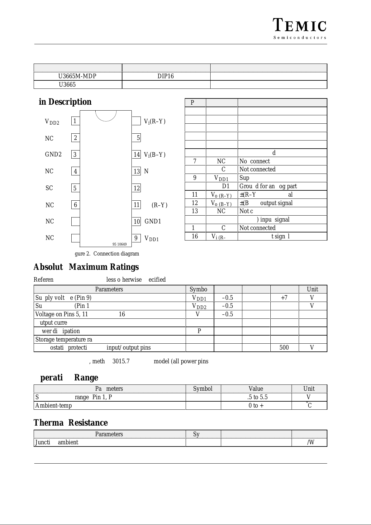
Pin Description
V
DD2
NC
GND2
NC
SC
NC
NC
NC
1
2
3
4
5
6
7
8
Figure 2. Connection diagram
95 10649
16
15
14
13
12
11
10
9
Vi(R–Y)
NC
(B–Y)
V
i
NC
(B–Y)
V
o
(R–Y)
V
0
GND1
V
DD1
Absolute Maximum Ratings
Reference point Pin 3, 10, unless otherwise specified
Parameters Symbol Min. Typ. Max. Unit
Supply voltage (Pin 9)
Supply voltage (Pin 1)
Voltage on Pins 5, 11, 12, 14 and 16
Output current, (Pin 11, Pin 12)
Power dissipation
Storage temperature range
Electrostatic protection* for input/ output pins
Pin Symbol Function
1
2
3
4
5
6
7
8
9
10
11
12
13
14
15
16
V
V
I
T
DD1
DD2
V
out
P
stg
V
DD2
NC
GND2
NC
SC
NC
NC
NC
V
DD1
GND1
Vo
(R–Y)
Vo
(B–Y)
NC
V
i (B–Y)
NC
V
i (R–Y)
n
Supply voltage for digital part
Not connected
Ground for digital part
Not connected
Sandcastle-pulse input
Not connected
Not connected
Not connected
Supply voltage for analog part
Ground for analog part
±(R–Y) output signal
±(B–Y) output signal
Not connected
±(B–Y) input signal
Not connected
±(R–Y) input signal
–0.5
–0.5
–0.5
+7
+7
V
S
20
1.1
–25
+150
500
V
V
V
mA
W
°C
V
* MIL standard 883D, method 3015.7 machine model (all power pins connected together)
Operating Range
Parameters Symbol Value Unit
Supply-voltage range (Pin 1, Pin 9)
Ambient-temperature range
T
V
amb
s
4.5 to 5.5
–10 to +70
Thermal Resistance
Parameters Symbol Value Unit
Junction ambient
2 (9)
R
thJA
80
TELEFUNKEN Semiconductors
Preliminary Information
V
°
C
K/W
Rev . A1, 17-Jul-96

Electrical Characteristics
Á
Á
Á
Á
Á
Á
Á
Á
Á
Á
Á
Á
Á
Á
Á
Á
Á
Á
Á
Á
Á
Á
Á
Á
Á
Á
Á
Á
Á
Á
Á
Á
Á
Á
Á
Á
Á
Á
Á
Á
Á
Á
Á
Á
VDD = 5.0 V, T
unless otherwise specified
Parameters Test Conditions / Pins Symbol Min. Typ. Max. Unit
DC-supply Pin 1, 9
Supply voltage (analog part)
Supply voltage (digital part)
Supply current (analog part)
Supply current (digital part)
Power dissipation
Color -ifference input signals Pin 14, 16
Input signal
БББББББ
(peak-to-peak value)
±(R–Y) PAL and NTSC
БББББББ
±(B–Y) PAL and NTSC
±(R–Y) SECAM
±(B–Y) SECAM
Input resistance
Input capacitance
Input clamping voltage
Color-difference output signals Pin 11, 12
Output signal
БББББББ
(peak-to-peak value) ±(R–Y)
±(B–Y)
Ratio of output amplitudes at
equal input signals
DC output voltage
Output resistance
Gain for PAL and NTSC
Gain for SECAM
Ratio of output signals for
БББББББ
adjacent time samples at
БББББББ
constant input signals
Noise voltage
(RMS value)
БББББББ
Delay of delayed signals
Delay of non-delayed signals
Transient time of delayed
signal
БББББББ
Transient time of
non-delayed signal
БББББББ
Sandcastle-pulse input Pin 5
Sandcastle frequency
Top pulse voltage
БББББББ
Internal slicing level
Input current
Input capacitance
= 25°C, reference point, Pin 3 and Pin 10 connected together, sandcastle frequency of 15.625 kHz;
amb
Pin 9
Pin 1
Pin 9
Pin 1
ББББББББ
ББББББББ
Pin 16
Pin 14
Pin 16
Pin 14
During clamping
Non color input level
during clamping
ББББББББ
All standards Pin 11
All standards Pin 12
Pin 11, 12
Pin 11, 12
Ratio V
Ratio V
V
SECAM signals,
Pin 11 / Pin 12
V
f = 10 kHz to 1 MHz
/ V
o
i
/ V
o
i
= 1.33Vpp,
i 14,16
ББББББББ
ББББББББ
= 0, R
i 14,16
ББББББББ
< 300
gen
W
Pin 11, 12
300 ns transient of SECAM
input signal, C
ББББББББ
= 22 pF
load
Pin 11, 12
300 ns transient of SECAM
input signal, C
ББББББББ
= 22 pF
load
Pin 11, 12
The leading edge of the burstkey pulse is used for timing
ББББББББ
V
DD1
V
DD2
I
S1
I
S2
P
ÁÁ
V
ÁÁ
i
V
i
V
i
V
i
R14, R
C14, C
V
14
V
16
ÁÁ
V
o
V
o
V11/V
V
11,12
R
11,12
G
v
G
v
V
(n)
ÁÁ
V
(n+1)
ÁÁ
V
noise
ÁÁ
t
d
t
d
t
tr
ÁÁ
t
tr
ÁÁ
f
SC
V
5
ÁÁ
V
slice
I
5
C
5
16
16
12
/
63.94
V5–1.5
4.5
4.5
5.0
5.0
3.5
1
30
ÁÁ
ÁÁ
ÁÁ
0.525
ÁÁ
0.665
1.05
1.33
1.45
ÁÁ
ÁÁ
1.05
1.33
–0.4
0
3.0
5.5
–0.5
ÁÁ
ÁÁ
ÁÁ
6.0
0
±0.1
ÁÁ
ÁÁ
ÁÁÁÁÁ
64.0
65
550
ÁÁ
ÁÁ
350
ÁÁ
14.0
ÁÁ3ÁÁ
ÁÁ
15.625
V5–1.25
U3665M
5.5
5.5
8.0
2
60
ÁÁ
1.0
ÁÁ
1.0
2.0
2.0
40
10
ÁÁÁÁÁ
+0.4
400
6.5
+0.5
ÁÁ
ÁÁ
1.2
64.06
ÁÁÁÁÁ
ÁÁÁÁÁ
17.0
Vs+0.7
ÁÁ
V5–1.0
10
10
V
V
mA
mA
mW
ÁÁ
V
ÁÁ
V
V
V
k
W
pF
V
V
V
dB
V
W
dB
dB
dB
ÁÁ
ÁÁ
mV
ÁÁ
µs
ns
ns
ns
kHz
V
ÁÁ
V
µA
pF
TELEFUNKEN Semiconductors
Rev . A1, 17-Jul-96
3 (9)
Preliminary Information
 Loading...