

TEMIC U2402B Datasheet
Fast Charge Controller for NiCd/NiMH Batteries
Description
The fast-charge battery controller circuit, U2402B, uses
bipolar technology. The IC enables the designer to create
an efficient and economic charge system. The U2402B
incorporates intelligent multiple-gradient batteryvoltage monitoring and mains phase control for power
management. With automatic top-off charging, the
integrated circuit ensures that the charge device stops
regular charging, before the critical stage of overcharging
is achieved. It has two LED driver indications for charge
and temperature status.
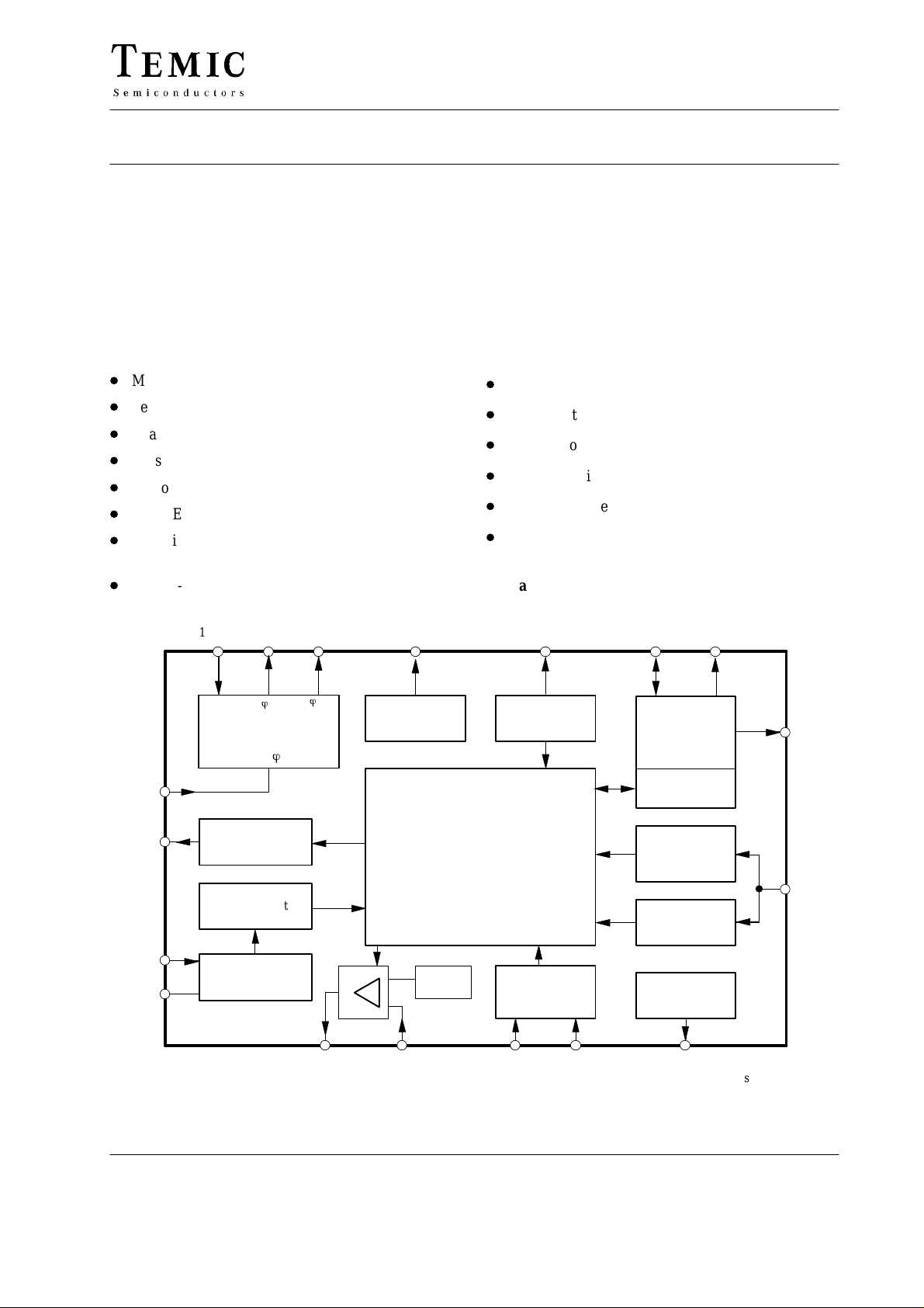
U2402B
Features
D
Multiple gradient monitoring
D
Temperature window (T
D
Exact battery voltage measurement without charge
D
Phase control for charge-current regulation
D
Top-off and trickle charge function
D
Two LED outputs for charge status indication
D
Disabling of d
2
V/dt2 switch-off criteria
min/Tmax
during battery formation
D
Battery-voltage check
18 (20)
4 (4)
Sync
17 (19)
ö
C
Phase control
V
ö
i
16 (18)
ö
R
)
6.5 V/10 mA
14 (15)
V
Ref
Applications
D
Portable power tools
D
Laptop/notebook personal computer
D
Cellular/cordless phones
D
Emergency lighting systems
D
Hobby equipment
D
Camcorder
Package: DIP18, SO20
13 (14)
Oscillator
12 (13)
Status control
Scan path
11 (12)
3 (3)
1 (1)
15 (17)
2 (2)
94 8585
Trigger output
Power - on control
Power supply
= 8 to 26 V
V
S
TELEFUNKEN Semiconductors
Rev . A3, 14-Nov-96
5 (5)
Control unit
Gradient
2
d
V/dt2 and –dV
160 mV
Ref
6 (6)
Figure 1. Block diagram
Temp. control
max
Sensor
T
7 (8) 8 (9)
Battery
detection
V
= 5 V
Ref
V
Monitor
Batt
0.1 to 4 V
Charge break
output
9 (10)
( ) SO 20, Pins 7 and 16 NC
10 (11)
1 (17)

U2402B
Pinning
Package: DIP18
Output
GND
LED2
V
ö
OP
OP
I
T
max
Sensor
t
p
Pin Description
Pin Symbol Function
1 Output Trigger output
1
2
3
4
i
5
O
6
7
8
9
93 7723 e
18
17
16
15
14
13
12
11
10
V
sync
ö
C
ö
R
V
S
V
Ref
Osc
S
TM.
LED1
V
Batt
2 GND Ground
3 LED2 Display output “Green”
4 V
5 OP
öiPhase angle control input voltage
Operational amplifier output
O
6 OPIOperational amplifier input
7 T
Maximum temperature
max
8 Sensor Temperature sensor
9 t
10 V
Charge break output
p
Battery voltage
Batt
11 LED1 LED display output “Red”
12 S
Test mode switch (status control)
TM.
13 Osc Oscillator
14 V
15 V
16
ö
Reference output voltage
Ref
Supply voltage
S
Ramp current adjustment –
R
resistance
17
18 V
ö
C
sync.
Ramp voltage – capacitance
Mains synchronization input
Package: SO20
Output
GND
LED2
V
ö
OP
OP
NC
T
max
Sensor
t
p
Pin Symbol Function
1 Output Trigger output
1
20
V
sync
2 GND Ground
3 LED2 Display output “Green”
ö
2
3
19
18
C
4 V
5 OP
ö
R
6 OPIOperational amplifier input
öiPhase angle control input voltage
Operational amplifier output
O
7 NC Not connected
4
i
17
V
S
8 T
Maximum temperature
max
9 Sensor Temperature sensor
5
O
6
I
7
8
9
16
15
14
13
12
NC
V
Ref
Osc
S
TM.
LED1
10 t
11 V
Charge break output
p
Battery voltage
Batt
12 LED1 LED display output “Red”
13 S
Test mode switch (status control)
TM.
14 Osc Oscillator
15 V
Reference output voltage
Ref
16 NC Not connected
17 V
18
ö
Supply voltage
S
Ramp current adjustment –
R
resistance
10
94 8594
11
V
Batt
19
20 V
ö
C
sync.
Ramp voltage – capacitance
Mains synchronization input
2 (17)
TELEFUNKEN Semiconductors
Rev . A3, 14-Nov-96
U2402B
Green
8
D
Red
7
D
W
5
R
1 k
S
V
From Pin 15
From
m
0.1 F
2
R
W
100 k
1
D
W
8
R
1 k
1
T
4
D
5
D
T2
/ R
T1
R
C
W
10
1
R
D
BC 308
m
0.22 F
W
560 k
6
13
R
W
10 k
6
R
Th1
D
10 nF
0
R
2x
10
2
C
R
3
3
W
560
11
0
C
13 12
W
270 k
2
14
C
4
R
17 16
10 nF
W
18
2.2 k
7
R
11
R
R
Th2
3
D
V
ϕ
ϕ
Sync
W
1 k
W
9
10 k
3
Status
control
Scan path
Oscillator
Ref
6.5 V/10 mA
R
C
To Pin 4
i
ϕ
V
Phase control
Battery
detection
Control unit
Trigger output
1
B1
R
B2
R
10
= 5 V
Monitor
Ref
V
Gradient
V
C
WW
1 k
10 k
7
C
Batt
V
& –dV
2
V/dt
2
d
Power supply
2
15
S
1
ch
I
m
4.7 F
0.1 to 4 V
= 8 to 26 V
S
V
m
470 F
W
16 k
output
Charge break
Sensor
max
T
Temp. control
Ref
160 mV
control
Power on
B3
R
7 8 9
5 6
4
NTC
DC
Battery
(4 cells)
(Pin 14)
To V
W
12 k
T1
R
m
1 F
m
1 F
Ref
R
R
sh
R
160 mV
R
T3
6
W
T2
100 k
m
8
C
0.1 F
W
24 k
4
C
R
C
W
10 k
W
0.2
94 8674
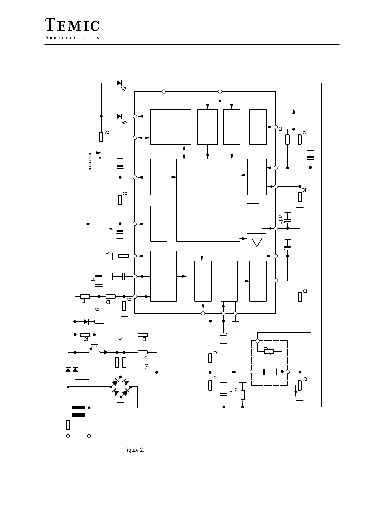
Mains
Figure 2. Block diagram with external circuit (DIP pinning)
TELEFUNKEN Semiconductors
Rev . A3, 14-Nov-96
3 (17)
U2402B
General Description
The integrated circuit, U2402B, is designed for charging
Nickel-Cadmium (NiCd) and Nickel-Metal-Hydride
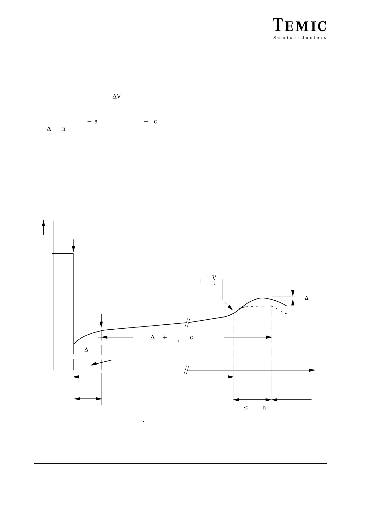
(NiMH) batteries. Fast charging results in voltage lobes
when fully charged (figure 3). It supplies two identifications (i.e., + d
operation at the proper time.
As compared to the existing charge concepts where the
charge is terminated * after voltage lobes * according
to – DV and temperature gradient identification, the
U2402B-C takes into consideration the additional
changes in positive charge curves, according to the second derivative of the voltage with respect to time
2
V/dt2). The charge identification is the sure method of
(d
switching off the fast charge before overcharging the battery. This helps to give the battery a long life by hindering
any marked increase in cell pressure and temperature.
Even in critical charge applications, such as a reduced
2
V/dt2, and – DV) to end the charge
charge current or with NiMH batteries where weaker
charge characteristics are present multiple gradient control results in very efficient switch-off.
An additional temperature control input increases not
only the performances of the charge switching characteristics but also prevents the general charging of a battery
whose temperature is outside the specified window .
A constant charge current is necessary for continued
charge-voltage characteristic. This constant current regulation is achieved with the help of internal amplifier phase
control and a simple shunt-current control technique.
All functions relating to battery management can be
achieved with dc-supply charge systems. A dc-dc-converter or linear regulator should take over the function of
power supply. For further information please refer to the
applications.
V
5 V
10
95 10172
Battery insertion
– DV
monitoring
Battery
formation
t1 = 5 min
Battery
voltage
check
–DV,
)
shorted batteries ignored
Fast charge rate I
2
d
dt
V
, active
2
O
Gradient recognition
2
d
V
)
2
dt
Top off
charge rate
1/4 I
O
t2 v 20 min
Trickle
charge rate
1/256 I
O
– DV
t
4 (17)
Figure 3. Charge function diagram, f
= 800 Hz
osc
TELEFUNKEN Semiconductors
Rev . A3, 14-Nov-96
U2402B
Flow Chart Explanation, f
= 800 Hz
osc
(Figures 2, 3 and 4)
Battery pack insertion disables the voltage lock at battery
detection input Pin 10. All functions in the integrated
circuit are reset. For further description, DIP-pinning is
taken into consideration.
Battery Insertion and –dV Monitoring
The charging procedure will be carried out if battery
insertion is recognised. If the polarity of the inserted
battery is not according to the specification, the fast
charge rate will stop immediately. After the polarity test,
if positive, the defined fast charge rate, I
first 5 minutes according to –dV monitoring. After
5 minutes of charging, the first identification control is
executed.
If the inserted battery has a signal across its terminal of
less than 0.1 V , then the char ging procedure is interrupted.
This means that the battery is defective i.e., it is not a
rechargeable battery – “shorted batteries ignored”.
Voltage and temperature measurements across the battery
are carried out during charge break interval (see figure 6),
i.e., currentless or idle measurements.
If the inserted battery is fully charged, the –dV control
will signal a charge stop after six measurements
(approximately 110 seconds). All the above mentioned
functions are recognised during the first 5 minutes
according to –dV method. During this time, +d
remains inactive. In this way the battery is protected from
unnecessary damage.
, begins for the
O
2
V/dt
Top-Off Charge Stage
By charge disconnection through the +d2V/dt
device switches automatically to a defined protective
top-off charge with a pulse rate of 1/4 I
= 5.12 s, period, T = 20.48 s).
t
p
The top-off charge time is specified for a time of
20 minutes @ 800 Hz.
2
(pulse time,
O
Trickle Charge Stage
When top-off charge is terminated, the device switches
automatically to trickle charge with 1/256 I
(tp = 5.12 s,
O
period = 1310.72 s). The trickle continues until the
battery pack is removed.
Basic Description
Power Supply, Figure 2
The charge controller allows the direct power supply of
8 to 26 V at Pin 15. Internal regulation limits higher input
voltages. Series resistance, R
current, I
resistance is recommended to suppress the noise signal,
2
even below 26 V limitation. It is calculated as follows:
R
1min
, to a maximum value of 25 mA. Series
S
–26 V
V
max
w
25 mA
, regulates the supply
1
mode, the
d2V/dt2-Gradient
If there is no charge stop within the first 5 minutes after
battery insertion, then d
In this actual charge stage, all stop-charge criteria are
active.
When close to the battery’s capacity limit, the battery
voltage curve will typically rise. As long as the +d
stop-charging criteria are met, the device will stop the fast
charge activities.
TELEFUNKEN Semiconductors
Rev . A3, 14-Nov-96
2
V/dt2 monitoring will be active.
2
V/dt
V
–8V
v
min
I
tot
R
1max
where
I
= IS + I
tot
V
max, Vmin
I
= Current consumption (IC) without load
S
2
I
= Current through resistance, R
RB1
+ I
RB1
1
= Rectified voltage
I1 = Trigger current at Pin 1
B1
5 (17)
U2402B
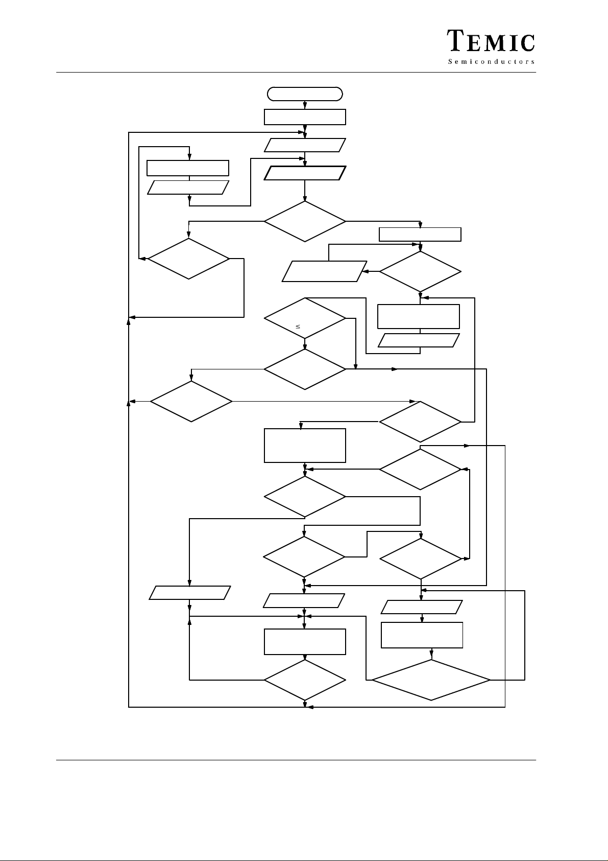
Start
turn on
Power on reset
LED2 on
Charge stop
LED1 blinking
Cell in
permissible
temperature
yes
no
*) 70 mV > V
range ?
Cell
inserted ?
*)
< 5 V
Batt
Cell insertion
no
no
no
yes
Cell
inserted ?
*)
LED1 on
LED2 off
V
Batt
4 V
v
yes
–dV
switch off
–dV and d
monitoring begins
no
2
V/dt2
Cell in
permissible
temperature
range ?
no
yes
yes
yes
Cell insertion reset
no
yes
Cell in
permissible
temperature
yes
Charging starts with
-dV monitoring
LED2 blinking
Charging
time reaches
5 min. ?
inserted ?
range ?
noyes
no
Cell
*)
6 (17)
93 7696 e
LED1 on
–dV
disconnect ?
yes
LED2 on
Trickle charging
with 1/256 I
yes
Cell
inserted ?
*)
no
Figure 4. Flow chart
2
no
disconnect ?
Top-off charging
O
yes
with 1/4 I
Timer 20 min exceeded
d
V/dt
yes
LED2 on
2
no
O
TELEFUNKEN Semiconductors
Rev . A3, 14-Nov-96
 Loading...