

TEMIC U2100B Datasheet
Timer Control for Triac and Relay
Description
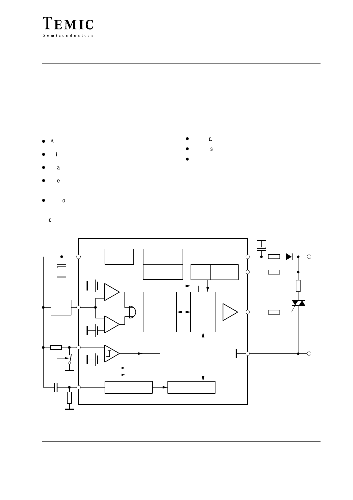
The timer control circuit, U2100B, uses bipolar technology. It has dif ferent mode selections (Zero voltage switch,
Phase control, Relay control). The output stage is
triggered according to input conditions. It can be used in
triac application for two or three wire system as a power
switch.
U2100B
Features
D
Adjustable and retriggerable tracking time
D
Window monitoring for sensor input
D
Enable input for triggering
D
Internal noise suppression (40 ms) and retrigger
blocking (640 ms)
D
Two or three wire application
Package: DIP8, SO8
Trigger
signal
8
C
2
6
0.5 V
Trigger
window
–V
Ref
Ref
+
–
+
–
Supply voltage
limitation
Voltage control
monitoring
Noise
suppression
40 ms
Retrigger
delay
640 ms
Applications
D
Motion detectors
D
Touch sensors
D
Timer
Sync
Control
logic
Mode
selection
2
4
3
–V
S
Output
C
1
R
1
D
1
R
sync
Load
R
G
L
Z
V
mains
0.6 V
5
En-
able
C
t
R
t
7
Ref
0.6 V
Ref
0.5 V
Ref
RC Oscillator Divider 1:2
TELEFUNKEN Semiconductors
Rev . A1, 30-May-96
ON
OFF
10
Figure 1. Block diagram with external circuit
95 9876
1
GND
N
1 (9)
U2100B
Pin Description
GND
–V
Output
Sync
1
2
S
3
4
95 9945
8
V
Ref
7
Osc
TRIG
6
EN
5
General Description
Monostable integrated power control circuit, U2100B,
can be used according to mode selection in relay’s or
triac’s applications. Beyond that, it can be used in triacapplication for two wire system as power switch, (being
the load in series to the switch) whereas the supply
voltage for the control unit is gained from phase rest angle
-operation).
(
a
min
L
Control
Pin Symbol Function
1 GND Reference point
2 –V
Supply voltage
S
3 Output Driver output
4 Sync Synchronisation and mode selection
5 EN Enable
6 TRIG Input trigger signal
7 Osc RC Oscillator
8 V
Reference voltage
Ref
For three wire switch, two modes of operations are
possible:
– Zero voltage switch operation for triac control
– Static operation for relay control
Mode Selection Pin 4 and Supply Voltage
Pin 2
Operation modes can be selected by external voltage at
the sync. input Pin 4 (clamping). Mode selection determines the current requirement of driver stage for relay’s
or triac’s and hence the selection of supply voltage.
Zero Voltage Switch Operation, Figure 4
Selection condition:
V
= internal sync limitation, without external clamping
4
V
0.85
M–VS
2I
X
tot
G
p
R
[
1
N
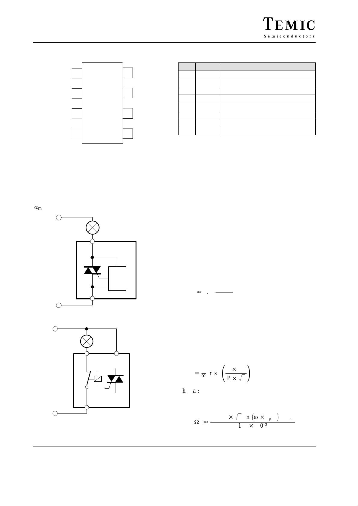
Figure 2. Two wire circuit
L
95 9949
I
= IS + Ip + I
tot
whereas:
= Supply current of IC without load
I
S
= Average trigger current I
I
P
I
= External circuit current requirement
X
= Mains voltage
V
M
Required firing pulse width t
Control
IL
tp+
2
w
arcsin
ǒ
P 2
V
M
Ǔ
Ǹ
whereas:
= Triac latching current
I
L
P = Power at load Z
N
Figure 3. Three wire circuit
95 9950
V
[
k
W][
R
sync
M
sinǒw t
2
1.8 10
Ǹ
[V]
Ǔ
[s]
–0.7
p
–2
–176
2 (9)
TELEFUNKEN Semiconductors
Rev . A1, 30-May-96
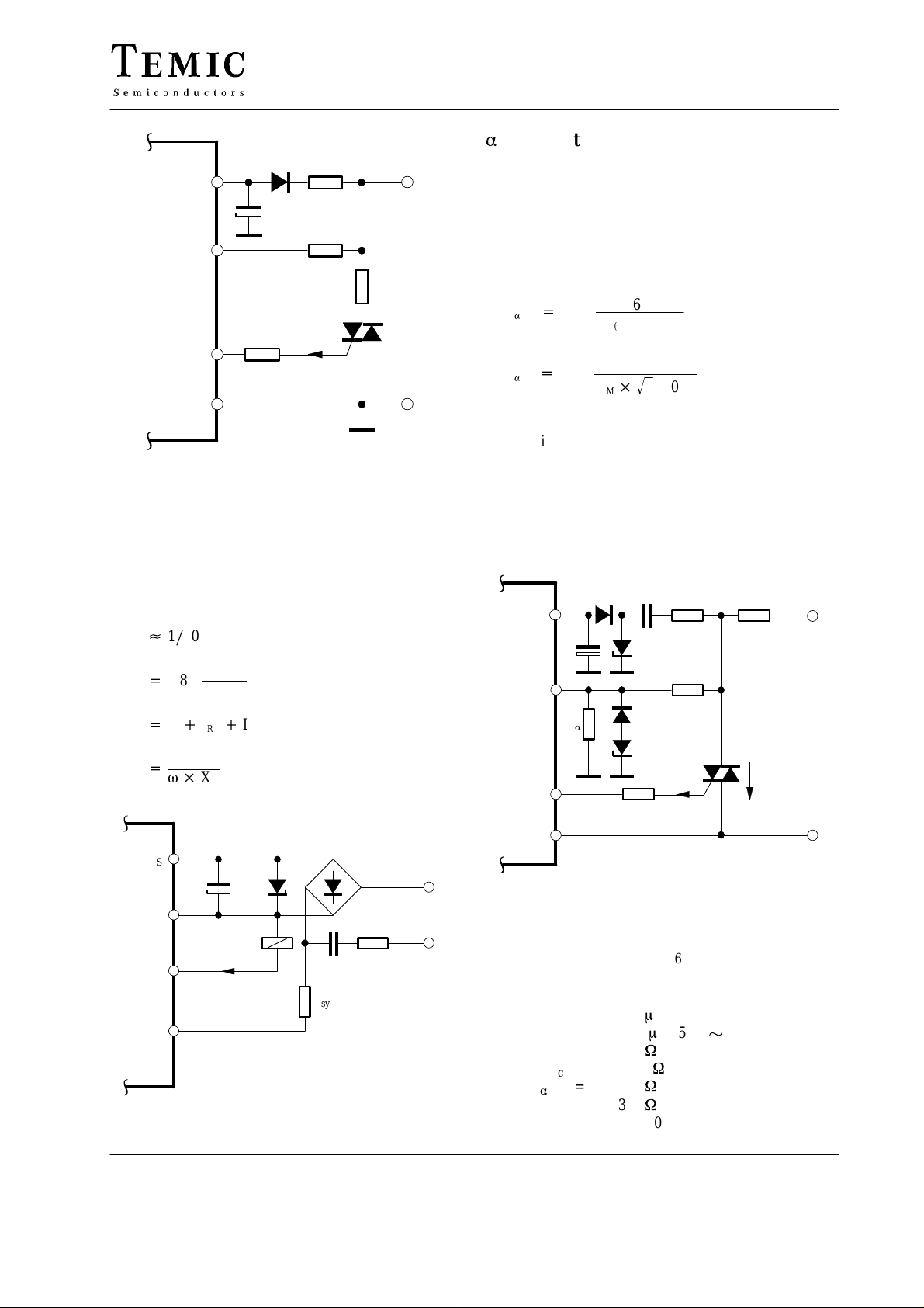
–V
Sync
U2100B
a
-operation, Figure 6
min
D
2
S
4
1
R
1
C
1
R
sync
L
Selection condition:
–V
= 6.5 to 7.8 V +V4 = int. limitation
4
3
Output
1
GND
95 9951
R
G
Figure 4.
DC Operation, Figure 5
Selection condition:
+V
= 6.1 V –V
4
whereas:
[1ń
R
0
Xc+
I
+
tot
C0+
–V
GND
Output
Sync
95 9952
0.85
IS)
w X
2
S
1
3
4
10 X
VM–V
I
1
C
1
Rel
4
c
I
tot
)
C
I
Rel
= int. limitation
S
I
X
BZX85C22V
Rel
Figure 5.
Z
I
G
C
o
R
sync
4xBYX86
R
o
V
M
N
N
V
M
230 V~
V
V
3.6 V
R(peak)
M
–3.6 V
10 V
2Ǹ–10 V
V
R(peak)
R
+
R
a
max
R
a
min
+
sync
R
sync
is the peak voltage of the rest phase angle, which
should be high enough to generate the supply voltage, V
D
1
IN 4007
2
–V
S
C
1
4
Sync
R
a
3
Output
1
GND
95 9953
L
C
= 100 mF/35 V
1
= 0.33 mF/250 V
C
o
= 390
R
o
= 220 k
R
sync
R
= 10 k
a
= 390
R
G
D
1 =
C
o
BZX85
C22V
1N4148
BZX55
6V8
R
G
Figure 6.
W
W
W
W
IN 4007
R
o
R
sync
I
G
Z
V
R(peak)
V
M
230 V~
.
S
L
N
TELEFUNKEN Semiconductors
Rev . A1, 30-May-96
3 (9)
 Loading...