

TEMIC U209B3 Datasheet
TELEFUNKEN Semiconductors
U209B3/ U209B3–FP
Preliminary Information
Rev. A1: 01.09.1995 1 (15)
Phase Control Circuit – Tacho Applications
Description:
The integrated circuit U209B3, is designed as a phase
control circuit in bipolar technology. It has also protection
circuit for the supply. Due to integration of many
functions, it leads to significant cost and space saving as
well as increased reliability . At the same time, it gives the
designer free hand to select varieties of regulators to
choose from and switching characteristics according to its
choice.
Features
Internal frequency to voltage converter
Externally controlled integrated amplifier
Automatic soft start with minimised ”dead time”
Voltage and current synchronisation
Retriggering
Triggering pulse typ. 155 mA
Internal supply voltage monitoring
Temperature compensated reference source
Current requirement ≤ 3 mA
Package: DIP14, SO16
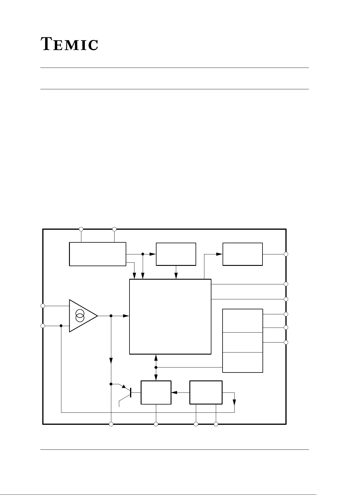
Control
amplifier
Voltage
monitoring
Supply
voltage
limitation
Reference
voltage
Output
pulse
Frequency
to voltage
converter
Phase
control unit
Soft start
10(10)
11(11) 12(12) 8(8) 7(7)
Voltage / Current
detector
Automatic
retriggering
14(16) 1(1)
4(4)
= f (V12)
95 10691
–V
S
GND
+
–
s
5(5)
6(6)
3(3)
2(2)
13(15)
9(9)
Figure 1. Block diagram – SO 16 in bracket
TELEFUNKEN Semiconductors
U209B3/ U209B3–FP
Preliminary Information
Rev. A1: 01.09.1995 3 (15)
95 10692
R
3
220 k
R
4
470 k
R
2
–V
S
3.3 nF
GND
C
1
22
25 V
C
10
2.2
16 V
R
10
220
M
R
1
18 k
BYT51J
D
1
2 W
AEG
TW11
N600
R
8
2 M
68 k
R
6
C
6
100 nF
2.2
16 V
C
7
C
8
220 nF
22 k
R
7
C
3
2.2
16 V
C
5
1 nF
R
5
1 k
Speed sensor
C
4
220 nF
L
N
V
M
=
230 V ~
Control
amplifier
Voltage
monitoring
Supply
voltage
limitation
Reference
voltage
Output
pulse
Frequency
to voltage
converter
Phase
control unit
Soft start
10
9
11 12 8 7
6
3
2
13
Voltage / Current
detector
Automatic
retriggering
14 1
5
4
= f (V
12
)
+
–
s
C
2
Actual
speed
voltage
680 k
R
11
100 k
C
9
2.2 /16 V
R
31
100 k
R
10
56 k
R
9
47 k
Set speed
voltage
F
F
F
F
F
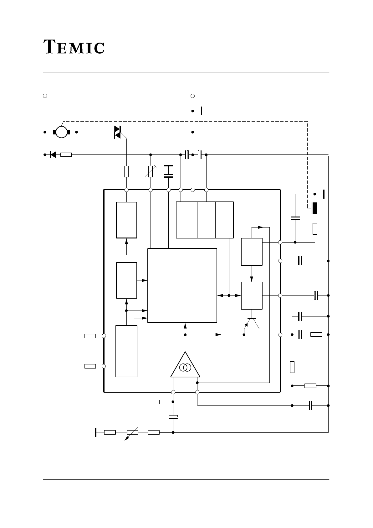
Figure 2. Block diagram with typical circuitry for speed regulation

TELEFUNKEN Semiconductors
U209B3/U209B3–FP
Preliminary Information
Rev. A1: 31.09.19954 (15)
Description
Mains Supply
The U209B is designed with voltage limiting and can
therefore be supplied directly from the mains. The supply
voltage between Pin 2 (+ pol/) and Pin 3 builds up
across D
1
and R
1
and is smoothed by C1. The value of the
series resistance can be approximated using (Figure 2):
VM – Vs
2 I
S
R1 =
Further information regarding the design of the mains
supply can be found in the data sheets in the appendix.
The reference voltage source on Pin 13 of typ. –8.9 V
is
derived from the supply voltage and represents the reference level of the control unit.
Operation using an externally stabilised DC voltage is not
recommended.
If the supply cannot be taken directly from the mains
because the power dissipation in R
1
would be too large,
then the circuit shown in the following Figure 3 should be
employed.
123
4
U21 1B
5
C
1
R
1
24 V~
~
95 10362
Figure 3. Supply voltage for high current requirements
Phase Control
The function of the phase control is largely identical to
that of the well known integrated circuit U211B. The
phase angle of the trigger pulse is derived by comparing
the ramp voltage, which is mains synchronised by the
voltage detector, with the set value on the control input
Pin 4. The slope of the ramp is determined by C
2
and its
charging current. The charging current can be varied
using R
2
on Pin 5. The maximum phase anglea
max
can
also be adjusted using R
2
.
When the potential on Pin 6 reaches the nominal value
predetermined at Pin 11, then a trigger pulse is generated
whose width t
p
is determined by the value of C
2
(the value
of C
2
and hence the pulse width can be evaluated by
assuming 8 ms/nF.
The current sensor on Pin 1 ensures that, for operation
with inductive loads, no pulse will be generated in a new
half cycle as long as current from the previous half cycle
is still flowing in the opposite direction to the supply
voltage at that instant. This makes sure that ”Gaps” in the
load current are prevented.
The control signal on Pin 11 can be in the range 0 V to
–7 V (reference point Pin 2).
If V
11
= –7 V then the phase angle is at maximum = a
max
i. e. the current flow angle is a minimum. The minimum
phase anglea
min
is when V
11
= V
pin2
.
Voltage Monitoring
As the voltage is built up, uncontrolled output pulses are
avoided by internal voltage surveillance. At the same
time, all of the latches in the circuit (phase control, soft
start) are reset and the soft–start capacitor is short
circuited. Used with a switching hysteresis of 300 mV,
this system guarantees defined start–up behaviour each
time the supply voltage is switched on or after short
interruptions of the mains supply .
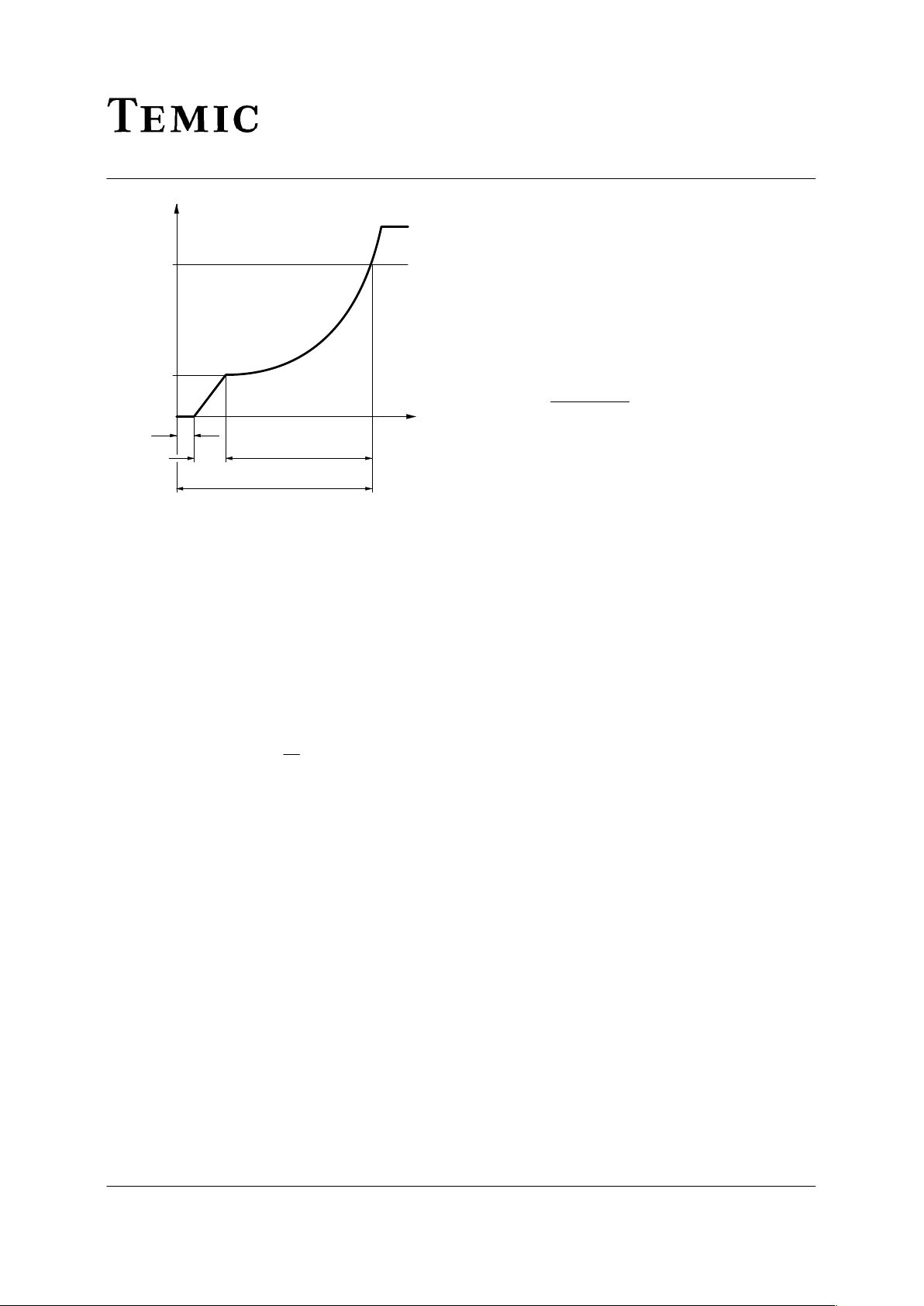
Soft–Start
As soon as the supply voltage builds up (t1), the integrated
soft–start is initiated. The figure below shows the
behaviour of the voltage across the soft–start capacitor
and is identical with the voltage on the phase control input
on Pin 11. This behaviour guarantees a gentle start–up for
the motor and automatically ensures the optimum run–up
time.
C
3
is first charged up to the starting voltage Vo with
typically 30 mA current (t
2
). By then reducing the
charging current to approx. 4 mA, the slope of the charging
function is substantially reduced so that the rotational
speed of the motor only slowly increases. The charging
current then increases as the voltage across C
3
increases
giving a progressively rising charging function which
more and more strongly accelerates the motor with
increasing rotational speed. The charging function
determines the acceleration up to the set–point. The
charging current can have a maximum value of 50 mA.
TELEFUNKEN Semiconductors
U209B3/ U209B3–FP
Preliminary Information
Rev. A1: 01.09.1995 5 (15)
V
C3
t
V
1
2
V
0
t
1
t
tot
t
2
t
3
95 10272
Figure 4. Soft–start
Frequency to Voltage Converter
The internal frequency to voltage converter
(f/V-converter) generates a DC signal on Pin 9 which is
proportional to the rotational speed using an AC signal
from a tacho–generator or a light beam whose frequency
is in turn dependent on the rotational speed. The high
impedance input with a switch–on threshold of typ. –
100 mV gives very reliable operation even when
relatively simple tacho–generators are employed. The
tacho-frequency is given by:
f =
n
60
n = revolutions per minute
p
= number of pulses per revolution
p[Hz]
The converter is based on the charge pumping principle.
With each negative half wave of the input signal, a
quantity of charge determined by C
5
is internally
amplified and then integrated by C
6
at the converter
output on Pin 9.
The conversion constant is determined
by C
5
, its charging voltage of Vch, R
6
(Pin 9) and the
internally adjusted charge amplification G
i
.
k = G
i
.
C
5
.
R
6
.
V
ch
The analog output voltage is given by
V
o
= k . f.
whereas: V
ch
= 6.7 V
G
i
= 8.3
The values of C
5
and C
6
must be such that for the highest
possible input frequency, the maximum output voltage
does V
0
does not exceed 6 V. While C
5
is charging up the
R
i
on Pin 8 is approx. 6 kΩ. T o obtain good linearity of the
f/V converter the time constant resulting from R
i
and C
5
should be considerably less (1/5) than the time span of the
negative half cycle for the highest possible input
frequency. The amount of remaining ripple on the output
voltage on Pin 9 is dependent on C
5
, C
6
and the internal
charge amplification.
∆V
o
=
G
i
. V
ch
.
C
5
C
6
The ripple ∆V
o
can be reduced by using larger values of
C
6
, however, the maximum conversion speed will than
also be reduced.
The value of this capacitor should be chosen to fit the
particular control loop where it is going to be used.
Control Amplifier
The integrated control amplifier with differential input
compares the set value (Pin 10) with the instantaneous
value on Pin 9
and generates a regulating voltage on the
output Pin 11 (together with external circuitry on Pin 12)
which always tries to hold the real voltage at the value of
the set voltages. The amplifier has a transmittance of typically 110 A/V and a bipolar current source output on Pin
11 which operates with typically ±100 A. The
amplification and frequency response are determined by
R
7
, C7, C
8
and R
8
(can be left out). For operation as a
power divider, C
4
, C5, R6, C6, R7, C7, C
8
and R
8
can be
left out. Pin 9
should be connected with Pin 11 and Pin 7
with Pin 2. The phase angle of the triggering pulse can be
adjusted using the voltage on Pin 10. An internal limiting
circuit prevents the voltage on Pin 11 from becoming
more negative than V
13
+ 1 V.
Pulse Output Stage
The pulse output stage is short circuit protected and can
typically deliver currents of 125 mA. For the design of
smaller triggering currents, the function I
GT
= f (RGT) has
been given in the data sheets in the appendix.
Automatic Retriggering
The automatic retriggering prevents half cycles without
current flow, even if the triacs is turned of f earlier e.g. due
to not exactly centred collector (brush lifter) or in the
event of unsuccessful triggering. If it is necessary, another
triggering pulse is generated after a time lapse of
t
PP
= 4.5 tP and this is repeated until either the triac fires
or the half cycle finishes.
TELEFUNKEN Semiconductors
U209B3/U209B3–FP
Preliminary Information
Rev. A1: 31.09.19956 (15)
General Hints and Explanation of Terms
To ensure safe and trouble–free operation, the following
points should be taken into consideration when circuits
are being constructed or in the design of printed circuit
boards.
The connecting lines from C
2
to Pin 6 and Pin 2 should
be as short as possible, and the connection to Pin 2
should not carry any additional high current such as
the load current. When selecting C
2
, a low tempera-
ture coefficient is desirable.
The common (earth) connections of the set–point gen-
erator, the tacho–generator and the final interference
suppression capacitor C
4
of the f/V converter should
not carry load current.
The tacho generator should be mounted without
influence by strong stray fields from the motor.
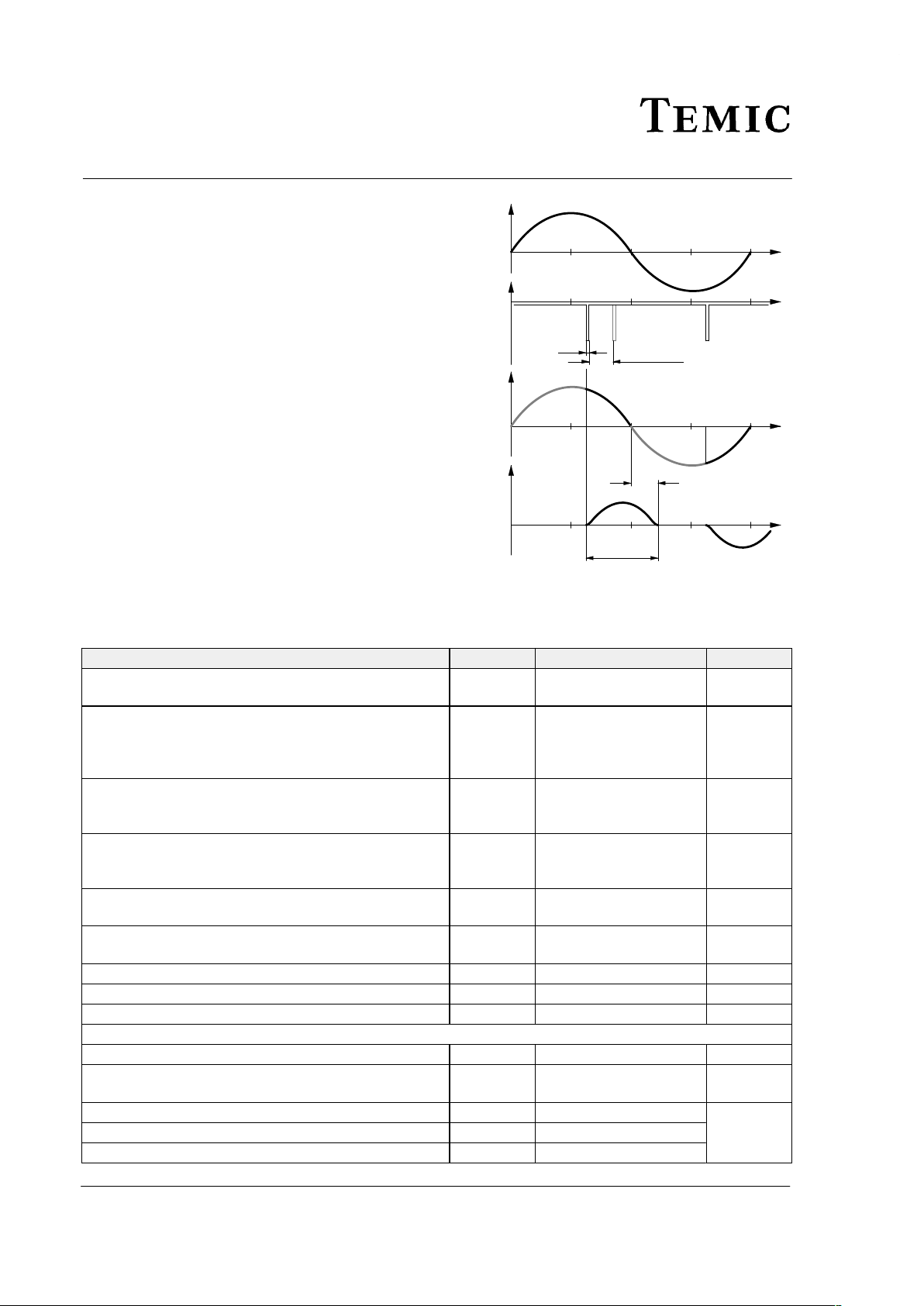
95 10716
V
V
GT
V
L
I
L
p/2 p 3/2p 2p
t
p
t
pp
= 4.5 t
p
f
F
Mains
Supply
Trigger
Pulse
Load
Voltage
Load
Current
Figure 5. Explanation of terms in phase relationship
Absolute Maximum Ratings
Reference point Pin 2, unless otherwise specified
Parameters Symbol Value Unit
Current requirement Pin 3
t ≤ 10 ms
–I
S
–i
S
30
100
mA
Synchronisation current Pin 1
Pin 14
t < 10 ms Pin 1
t < 10 ms Pin 14
I
syncI
I
syncV
±i
i
±i
v
5
5
35
35
mA
f/V converter:
Input current Pin 7
t < 10 ms
I
eff
±i
i
3
13
mA
Phase control: Pin 11
Input voltage
Input current
–V
I
±I
I
0 to 7
500
V
mA
Soft–start:
Input voltage Pin 12
–V
I
|V13| to 0 V
Pulse output:
Reverse voltage Pin 4
V
R
V
S
to 5 V
Amplifier
Input voltage Pin 10 –V
I
|VS|
Pin 8 open Pin 9 –V
I
|V13| to 0 V
Reference voltage source
Output current Pin 13 I
o
7.5 mA
Power dissipation T
amb
= 45 °C
T
amb
= 80 °C
P
tot
570
320
mW
Storage temperature range T
stg
–40 to +125 °C
Junction temperature T
j
125
Ambient temperature range T
amb
–10 to +100
 Loading...