

TEMIC U208B Datasheet
Open Loop Phase Control Circuit
Description
The integrated circuit, U208B, is designed as a phase control circuit in bipolar technology with internal
supply-voltage monitoring. As the voltage is built up, uncontrolled output pulses are avoided by internal
Features
D
Automatic retriggering
D
Triggering pulse typ. 125 mA
D
Voltage and current synchronisation
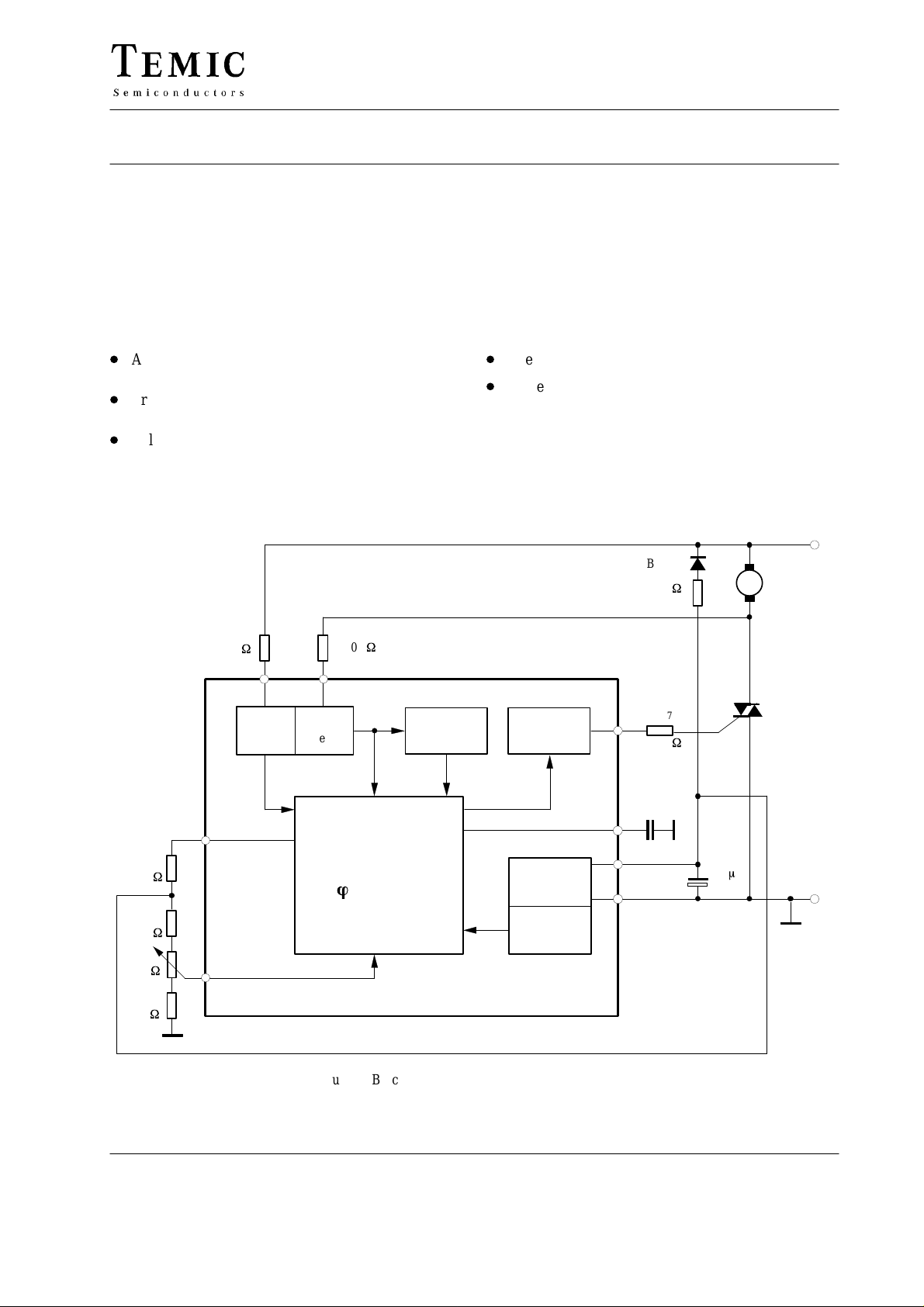
Block Diagram
monitoring. Furthermore, it has internal-current and voltage synchronisation. It is recommended as a low cost
open-loop control.
D
D
Package: DIP8
U208B
Internal supply voltage monitoring
Current requirement ≤ 2.5 mA
180 k
18 k
100 k
120 k
V
=
M
230 V ~
N
L
D
BYT77
18 kW/
2 W
R
3
220 kW/
0.5 W
7
Voltage
detector
4
R
2
W
R
6
W
W
R
5
W
6
R
4
470 kW/
0.5 W
8
Current
detector
Phase
control unit
ö
= f (V6)
Automatic
retriggering
Output
pulse
Supply
voltage
limitation
Voltage
monitoring
95 11224
R
10 nF
C
2
–V
GND
S
180
7
W
C
3
5
2
1
1
M
R
1
TIC
236N
22 mF/
1
25 V
TELEFUNKEN Semiconductors
Rev . A1, 28-May-96
Figure 1. Block diagram for simple phase control system
1 (7)
U208B
Description
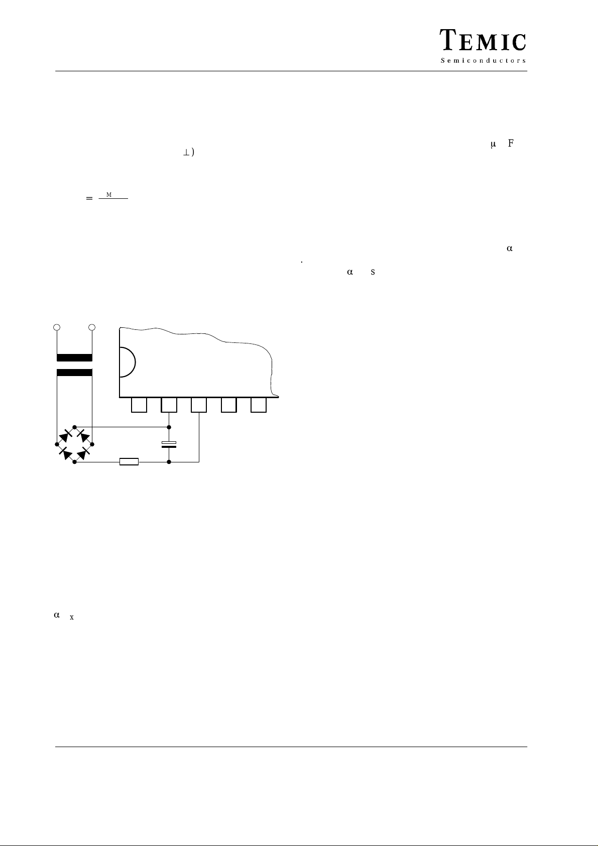
Mains Supply
The U208B is fitted with voltage limiting and can therefore be supplied directly from the mains. The supply
voltage between Pin 1 (+ pol/ă) and Pin 2 builds up
and R
across D
1
series resistance can be approximated using figure 1:
+
R
1
Further information regarding the design of the mains
supply can be found in the data sheets in the appendix.
Operation using an externally stabilized DC voltage is not
recommended.
If the supply cannot be taken directly from the mains
because the power dissipation in R
then the circuit shown in the following figure 2 should be
employed.
~
24 V~
and is smoothed by C1. The value of the
1
VM–V
S
2I
S
would be too large,
1
123
4
5
When the potential on Pin 5 reaches the given value of
Pin 6, then a trigger pulse is generated whose width t
determined by the value of C
(the value of C
2
and hence
2
is
p
the pulse width can be evaluated by assuming 8 ms/nF).
The current sensor on Pin 8 ensures that, for operation
with inductive loads, no pulse will be generated in a new
half cycle as long as the current from the previous half
cycle is still flowing in the opposite direction to the supply voltage at that instant. This makes sure that ”Gaps” in
the load current are prevented. The control signal on Pin
6 can be in the range 0 V to –7 V (reference point Pin 1).
If V
= –7 V then the phase angle is at maximum =
pin6
a
max
i.e., the current flow angle is a minimum. The minimum
phase angle
a
min
is when V
pin6
= V
pin1
.
Voltage Monitoring
As the voltage is built up, uncontrolled output pulses are
avoided by internal voltage surveillance. At the same
time, all of the latches in the circuit are reset. Used with
a switching hysteresis of 300 mV, this system guarantees
defined start–up behavior each time the supply voltage is
switched on ,or after short interruptions of the mains
supply.
Pulse Output Stage
C
R
1
Figure 2. Supply voltage for high current requirements
1
95 10362
Phase Control
The function of the phase control is largely identical to
that of the well known component TEA1007. The phase
angle of the trigger pulse is derived by comparing the
ramp voltage, which is mains synchronized by the voltage
detector, with the nominal value predetermined at the
control input Pin 6. The slope of the ramp is determined
and its charging current. The charging current can
by C
2
be varied using R
can also be adjusted using R2.
a
max
on Pin 4. The maximum phase angle
2
The pulse output stage is short circuit protected and can
typically deliver currents of 125 mA. For the design of
smaller triggering currents, the function I
= f (RGT) has
GT
been given in the data sheets in the appendix. In contrast
to the TEA1007, the pulse output stage of the U 208 B has
no gate bypass resistor.
Automatic Retriggering
The automatic retriggering prevents half cycles without
current flow, even if the triacs is turned of f earlier e.g. due
to a collector which is not exactly centered (brush lifter)
or in the event of unsuccessful triggering. If it is necessary, another triggering pulse is generated after a time
lapse of t
triac fires or the half cycle finishes.
= 4.5 tp and this is repeated until either the
pp
2 (7)
TELEFUNKEN Semiconductors
Rev . A1, 28-May-96
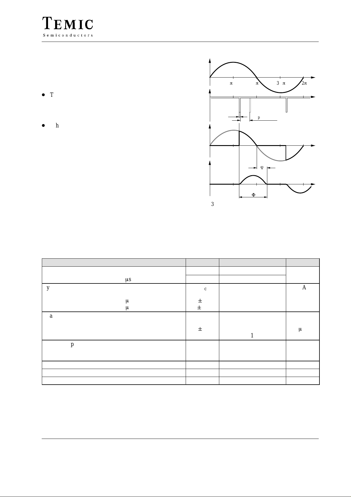
General Hints and Explanation of Terms
q
To ensure safe and trouble–free operation, the following
points should be taken into consideration when circuits
are being constructed or in the design of printed circuit
boards.
Mains
Supply
U208B
V
p
/2
p
3/2
95 10716
p
2
p
D
The connecting lines from C
to Pin 5 and Pin 1 should
2
be as short as possible, and the connection to Pin 1
should not carry any additional high current such as
e.g. the load current.
D
When selecting C
, a low temperature coefficient is
2
Trigger
Pulse
desirable.
Load
Voltage
Load
Current
Absolute Maximum Ratings
Reference point Pin 1, unless otherwise specified
Parameters Symbol Value Unit
Current requirement Pin 2 –I
t ≤ 10 ms
Synchronisation current Pin 8
Pin 7
t < 10 ms Pin 8
t < 10 ms Pin 7
Phase control
Input voltage Pin 6
Input current Pin 6
Pin 4
Power dissipation
T
= 45°C
amb
T
= 80°C
amb
Storage temperature range T
Junction temperature T
Ambient temperature range T
V
GT
t
p
V
L
I
L
Figure 3. Explanation of terms in phase relationship
S
–i
s
I
syncI
I
syncV
"
i
I
"
i
V
–V
I
"
I
I
I
I
P
tot
t
= 4.5 t
pp
p
ö
F
30 mA
100
5
5
35
35
0 to 7
500
1
530
mA
V
m
mA
mW
300
stg
j
amb
–40 to +125 °C
125 °C
–10 to +100 °C
A
TELEFUNKEN Semiconductors
Rev . A1, 28-May-96
3 (7)
 Loading...