

TEMIC U2010B Datasheet
Phase Control Circuit for Current Feedback
Description
The U2010B is designed as a phase-control circuit in
bipolar technology. It enables load-current detection and
has a soft-start function as well as reference voltage
Features
D
Full wave current sensing
D
Mains supply variation compensated
D
Programmable load-current limitation
with over- and high-load output
D
Variable soft-start
D
Voltage and current synchronization
D
Automatic retriggering switchable
D
Triggering pulse typical 125 mA
output. Motor control with load-current feedback and
overload protection are preferred applications.
D
Internal supply voltage monitoring
D
Current requirement v 3 mA
D
Temperature compensated reference voltage
Applications
D
Advanced motor control
D
Grinder
D
Drilling machine
U2010B
Package: DIP16, SO16
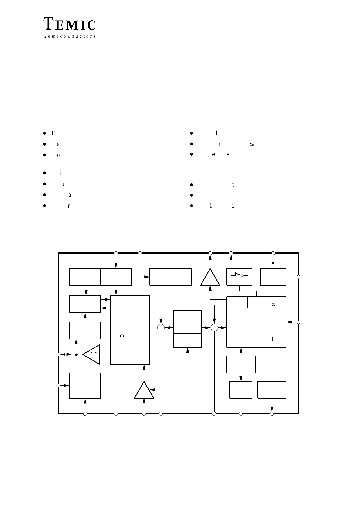
Block Diagram
96 11646
Limiting
detector
Automatic
retriggering
Current
detector
16
Pulse
output
Load
1
current
detector
15
Voltage
detector
control unit
Phase
ö
= f (V
Level
shift
14 13 12
Overload
Mains voltage
)
4
compensation
Output
–
12
Full wave
rectifier
High load
+
monitoring
100% 70%
Programmable
overload
protection
Voltage
Soft
start
11
Supply
voltage
a
max
Auto–
start
I
max
Reference
voltage
10
GND
A
B
9
C
2
3 5 67 8
TELEFUNKEN Semiconductors
Rev . A1, 28-May-96
4
Figure 1. Block diagram
1 (12)
U2010B
C
1
m
22 F
Mode
B
C
A
1
S
3
D
1
D
/2 W
W
18 k
LED
BYT51K
8
R
1
R
a
2
R
W
470 k
max
W
330 k
10
GND
S
V
Overload
14 13 12 11
15
Supply
voltage
High load
compensation
Mains voltage
Voltage
detector
detector
Limiting
9
B
A
max
a
100% 70%
Output
Automatic
retriggering
C
max
I
Auto–
start
overload
protection
Programmable
+
2
rectifier
1
Full wave
–
)
4
= f (V
Phase
ö
control unit
Current
detector
Voltage
monitoring
Reference
Soft
Level
Load
current
96 11647
voltage
m
2
C
4.7 F
start
threshold
Overload
11
W
R
1 M
5
C
m
m
0.1 F
0.15 F
C
shift
3 5 67 8
24
detector
3
C
10 nF
1
P
4
7
C
Set point
W
50 k
10
R
m
1 F
W
R78.2 k
W
100 k
Load current
compensation
Load
230 V ~
TIC
226
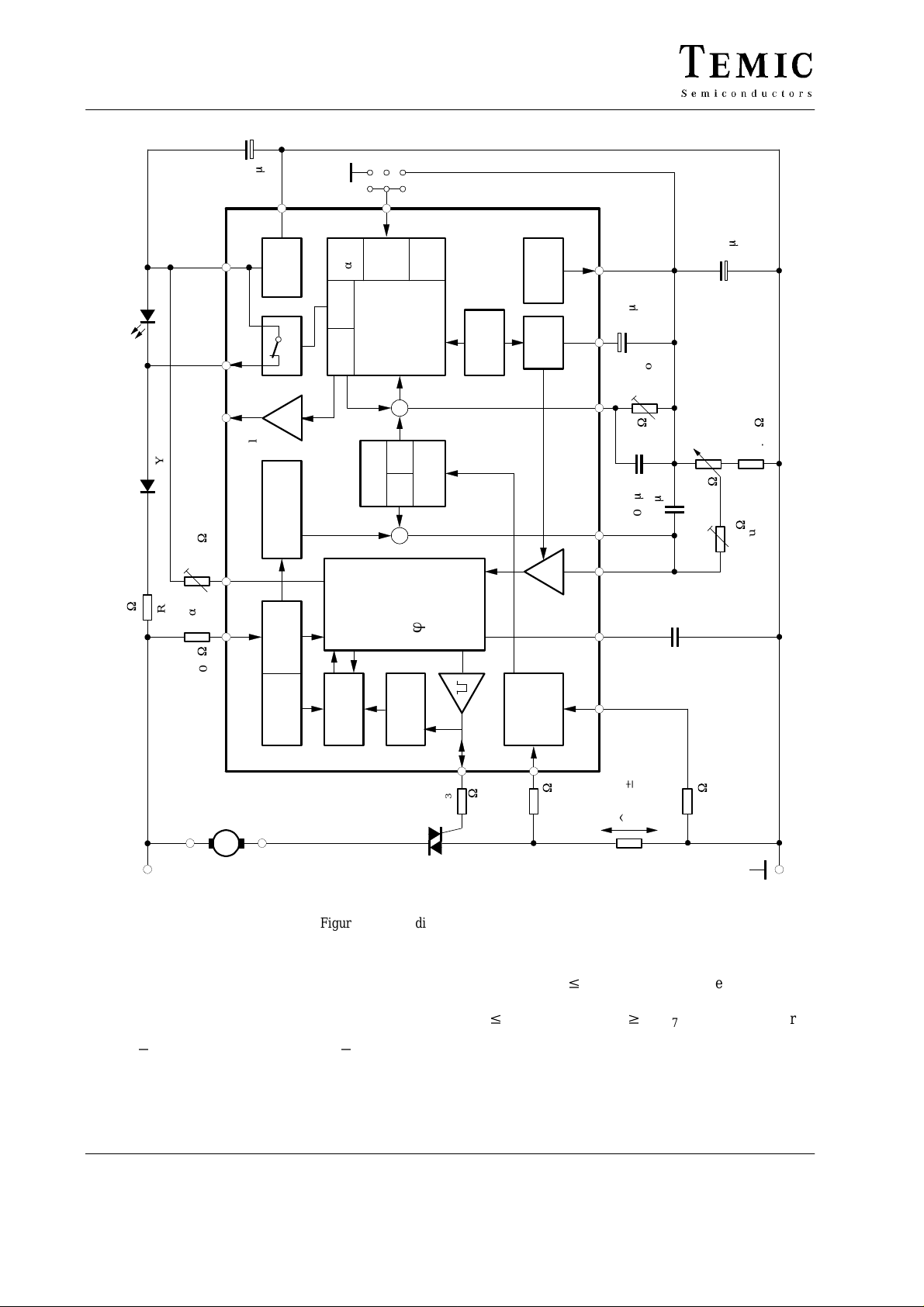
Figure 2. Block diagram with external circuit
General Description
Mains Supply
The U2010B contains voltage limiting and can be
connected with the mains supply via D
voltage * between Pin 10 and Pin 11 * is smoothed
.
by C
1
2 (12)
and R1. Supply
1
16
W
3
R
180
In the case of V
1
W
4
R
3.3 k
v (70% of overload threshold voltage),
6
$
= 250 mV
(R6)
^
V
6
R
W
5
R
3.3 k
Pins 11 and 12 are connected internally whereby
v 1.2 V. When V6 w V
V
sat
flows across D
.
3
, the supply current
T70
TELEFUNKEN Semiconductors
Rev . A1, 28-May-96
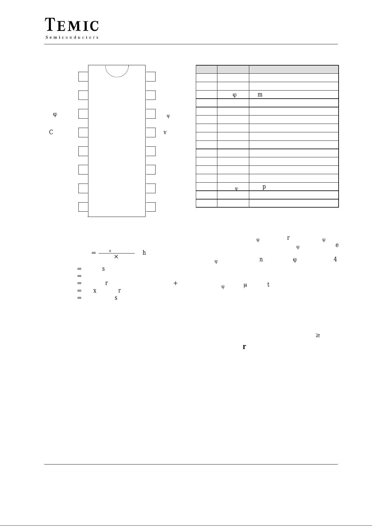
Pin Description
I
sense
I
sense
C
ö
Control
Comp.
I
Load
C
soft
V
Ref
1
2
3
4
5
6
7
8
16
15
14
13
12
11
10
9
Output
V
Sync.
V
R
ö
Overload
High load
V
S
GND
Mode
U2010B
Pin Symbol Function
1 I
2 I
sense
sense
3 C
4 Control Control input
5 Comp. Compensation output
6 I
7 C
8 V
Load
soft
Ref
9 Mode Mode selection
10 GND Ground
11 V
12 High load High load indication
13 Overload Overload indication
14 V
15 V
R
Sync.
16 Output Trigger output
Load current sensing
Load current sensing
ö
Ramp voltage
Load current limitation
Soft start
Reference voltage
Supply voltage
S
Ramp current adjust
ö
Voltage synchronization
95 11406
Series resistance R1 can be calculated as follows:
V
–V
V
mains
V
Smax
I
tot
I
Smax
I
x
R
+
+
+
+
+
1max
mains
+
Mains supply voltage
Maximum supply voltage
Total current consumption = I
Maximum current consumption of the IC
Current consumption of the
2 I
Smax
tot
whereas
Smax
)I
x
external components
Voltage Monitoring
As the voltage is built up, uncontrolled output pulses are
avoided by internal voltage monitoring. Apart from that
all the latches in the circuit (phase control, load limit
regulation) are reset and the soft-start capacitor is short
circuited. This guarantees a specified start-up behavior
each time the supply voltage is switched on or after short
interruptions of the mains supply. Soft-start is initiated
after the supply voltage has been built up. This behavior
guarantees a gentle start-up for the motor and automatically ensures the optimum run-up time.
Phase Control
The function of the phase control is largely identical to the
well known IC family U211B. The phase angle of the
trigger pulse is derived by comparing the ramp voltage V
which is mains synchronized by the voltage detector with
the set value on the control input, Pin 4. The slope of the
ramp is determined by C
charging current can be varied using R
maximum phase angle, α
using R
(minimum current flow angle
ö
and its charging current Iö. The
ö
can also be adjusted by
max,
at Pin 14. The
ö
ö
) see figure 4.
min
When the potential on Pin 3 reaches the set point level of
Pin 4, a trigger pulse width, t
value of C
(tp = 9 ms/nF). At the same time, a latch is set
ö
, is determined from the
p
with the output pulse, as long as the automatic
retriggering has not been activated, then no more pulses
can be generated in that half cycle. Control input at Pin 4
(with respect to Pin 10) has an active range from
to –1 V. When V4 = V8, then the phase angle is at its
V
8
maximum, α
The minimum phase angle, α
i.e., the current flow angle is minimum.
max,
is set with V4 w –1 V.
min,
Automatic Retriggering
The current-detector circuit monitors the state of the triac
after triggering by measuring the voltage drop at the triac
gate. A current flow through the triac is recognized, when
the voltage drop exceeds a thres hold level of typ. 40 mV.
If the triac is quenched within the relevant half-wave after
triggering; for example owing to low load currents before
or after the zero crossing of current wave or; for commutator motors, owing to brush lifters. Then the automatic
retriggering circuit ensures immediate retriggering, if
necessary with a high repetition rate, t
3
remains reliably triggered.
, until the triac
pp/tp
TELEFUNKEN Semiconductors
Rev . A1, 28-May-96
3 (12)
U2010B
Current Synchronization
Current synchronization fulfils two functions:
*
Monitoring the current flow after triggering.
In case the triac extinguishes again or it does not switch
on, automatic triggering is activated until the
triggering is successful.
*
Avoiding a triggering due to inductive load.
In the case of inductive load operation the current
synchronization ensures that in the new half wave no
pulse is enabled as long as there is a current available
which from the previous half-wave, which flows from
the opposite polarity to the actual supply voltage.
A special feature of the integrated circuit is the
realization of this current synchronization. The device
evaluates the voltage at the pulse output between gate and
reference electrode of the triac. This results in saving
separate current synchronization input with specified
series resistance.
Voltage Synchronization with Mains Voltage
Compensation
The voltage detector synchronizes the reference ramp
with the mains-supply voltage. At the same time, the
mains dependent input current at Pin 15 is shaped and
rectified internally. This current activates the automatic
retriggering and at the same time is available at Pin 5. By
suitable dimensioning, it is possible to attain the specified
compensation effect. Automatic retriggering and mains
voltage compensation are not activated until |V
increases to 8 V. Resistance, R
defines the width of
sync.
the zero voltage cross over pulse, synchronization
current, and hence the mains supply voltage
compensation current.
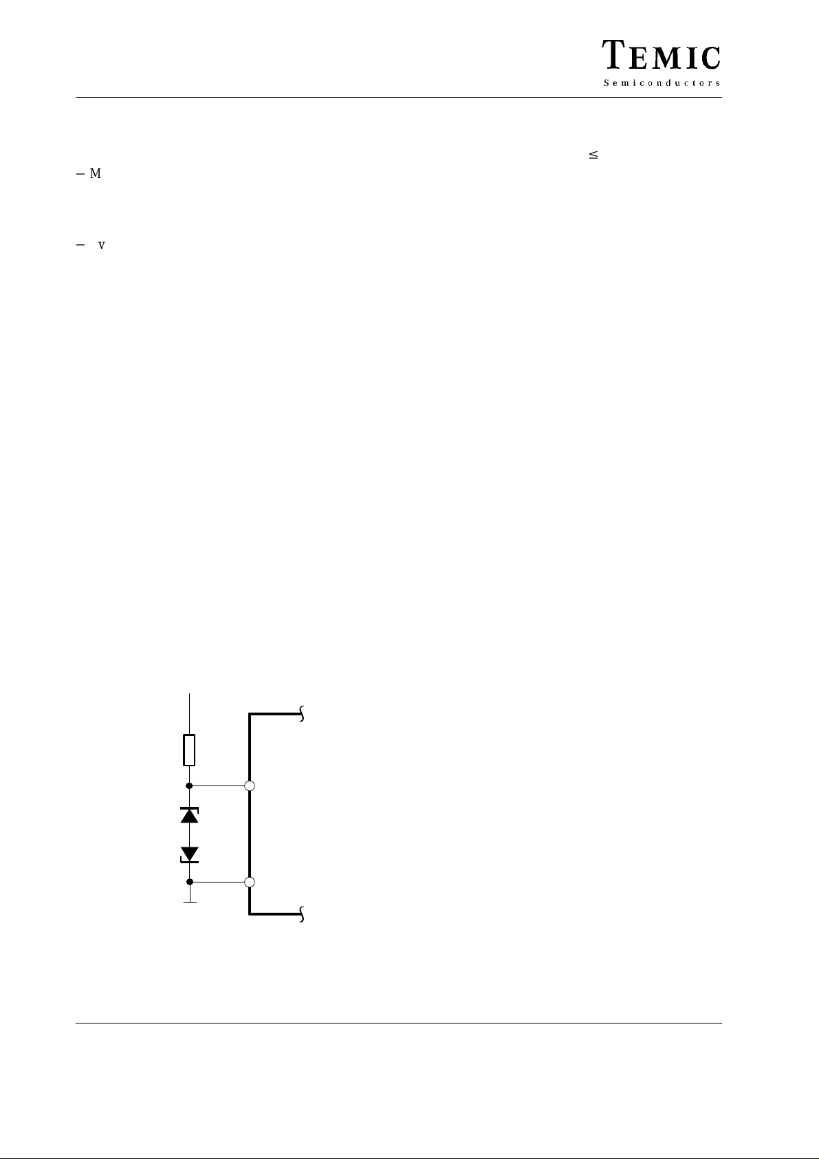
Mains
96 11648
– 10|
15
If the mains voltage compensation and the automatic
retriggering are not required, both functions can be
suppressed by limiting |V
| v 7 V (figure 3).
15 – 10
Load Current Compensation
The circuit continuously measures the load current as a
voltage drop at resistance R
. The evaluation and use of
6
both half waves results in a quick reaction to load current
change. Due to voltage at resistance R
, there is a
6
difference between both input currents at Pins 1 and 2.
This difference controls the internal current source,
whose positive current values are available at Pins 5
and 6. The output current generated at Pin 5 contains the
difference from the load-current detection and from the
mains-voltage compensation (see figure 1).
The effective control voltage at Pin 4 is the final current
at Pin 5 together with the desired value network. An
increase of mains voltage causes the increase of control
angle α, an increase of load current results in a decrease
in the control angle. This avoiding a decrease in
revolution by increasing the load as well as the increase
of revolution by the increment of mains supply voltage.
Load Current Limitation
The total output load current is available at Pin 6. It
results in a voltage drop across R
of the load current reaches about 70% of the threshold
value (V
) i.e., ca. 4.35 V at Pin 6, it switches the high
T70
load comparator and opens the switch between Pins 11
and 12. By using an LED between these pins, (11 and 12)
a high load indication can be realized.
If the potential at Pin 6 increases to ca. 6.2 V (= V
it switches the overload comparator. The result is
programmable at Pin 9 (operation mode).
. When the potential
11
T100
),
4 (12)
2x
BZX55
C6V2
R
2
15
U2010B
Mode selection:
a) α
(V9 = 0)
max
In this mode of operation, after V
threshold V
, Pin 13 switches to –V
T100
has reached the
6
(Pin 11) and
S
Pin 6 to GND (Pin 10). A soft-start capacitor is then
shorted and the control angle is switched to α
max
.
This position is maintained until the supply voltage
is switched off. The motor can be started again with
10
soft-start function when the power is switched on
again. As the overload condition switches Pin 13 to
Pin 11, it is possible to set in a smaller control angle,
, by connecting a further resistance between
α
max
Figure 3.
Pins 13 and 14.
TELEFUNKEN Semiconductors
Rev . A1, 28-May-96
 Loading...