

TEMIC TSC80C51XXX-L16MI-883, TSC80C51XXX-L16MH-883, TSC80C51XXX-L16MG-883, TSC80C51XXX-L20MI-883, TSC80C51XXX-L20MH-883 Datasheet
...
TSC80C31/80C51
Rev. E (14 Jan.97)
1
MATRA MHS
Description
The TSC80C31/80C51 is high performance SCMOS
versions of the 8051 NMOS single chip 8 bit µC.
The fully static design of the TSC80C31/80C51 allows to
reduce system power consumption by bringing the clock
frequency down to any value, even DC, without loss of
data.
The TSC80C31/80C51 retains all the features of the 8051
: 4 K bytes of ROM ; 128 bytes of RAM ; 32 I/O lines ;
two 16 bit timers ; a 5-source, 2-level interrupt structure
; a full duplex serial port ; and on-chip oscillator and clock
circuits.
In addition, the TSC80C31/80C51 has two
software-selectable modes of reduced activity for further
reduction in power consumption. In the Idle Mode the
CPU is frozen while the RAM, the timers, the serial port,
and the interrupt system continue to function. In the
Power Down Mode the RAM is saved and all other
functions are inoperative.
The TSC80C31/80C51 is manufactured using SCMOS
process which allows them to run from 0 up to 44 MHz
with VCC = 5 V. The TSC80C31/80C51 is also available
at 20 MHz with 2.7 V < Vcc < 5.5 V.
TSC80C31/80C51-L16 : Low power version
Vcc : 2.7–5.5 V Freq : 0–16 MHz
TSC80C31/80C51-L20 : Low power version
Vcc : 2.7–5.5 V Freq : 0–20 MHz
TSC80C31/80C51-12 : 0 to 12 MHz
TSC80C31/80C51-20 : 0 to 20 MHz
TSC80C31/80C51-25 : 0 to 25 MHz
TSC80C31/80C51-30 : 0 to 30 MHz
TSC80C31/80C51-36 : 0 to 36 MHz
TSC80C31/80C51-40 : 0 to 40 MHz
TSC80C31/80C51-44 : 0 to 44 MHz*
* Commercial and Industrial temperature range only. For other speed
and range please consult your sale office.
Features
Power control modes
128 bytes of RAM
4 K bytes of ROM (TSC80C31/80C51)
32 programmable I/O lines
Two 16 bit timer/counter
64 K program memory space
64 K data memory space
Fully static design
0.8 µm CMOS process
Boolean processor
5 interrupt sources
Programmable serial port
Temperature range : commercial, industrial, automotive and
military
Optional
Secret ROM : Encryption
Secret TAG : Identification number
CMOS 0 to 44 MHz Single-Chip 8 Bit Microcontroller
TSC80C31/80C51
Rev. E (14 Jan.97)
2
MATRA MHS
Interface
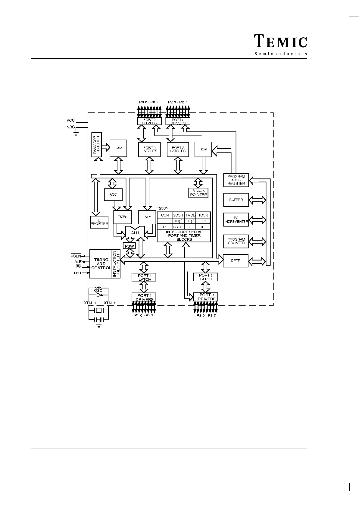
Figure 1. Block Diagram
TSC80C31/80C51
Rev. E (14 Jan.97)
3
MATRA MHS
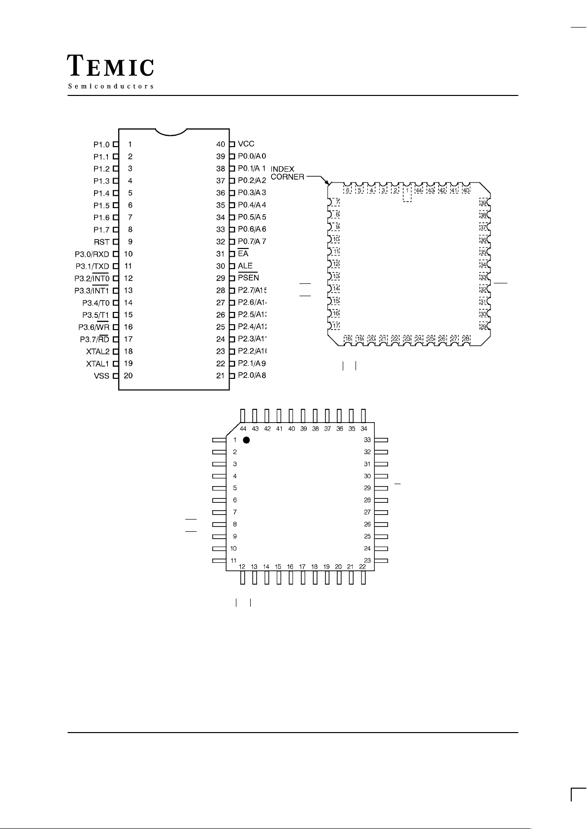
Figure 2. Pin Configuration
Diagrams are for reference only. Packages sizes are not to scale.
P1.4
P1.3
P1.2
P1.1
P1.0NCVCC
P0.0/A0
P0.1/A1
P0.2/A2
P0.3/A3
P0.4/A4P1.5
P1.6
P1.7
RST
RxD/P3.0
NC
TxD/P3.1
INT0/P3.2
INT1/P3.3
T0/P3.4
T1/P3.5
P0.5/A5
P0.6/A6
P0.7/A7
EA
NC
ALE
PSEN
P2.7/A15
P2.6/A14
P2.5/A13
WR/P3.6
RD/P3.7
XTAL2
XTAL1
VSS
NC
P2.0/A8
P2.1/A9
P2.2/A10
P2.3/A11
P2.4/A12
15
P
16
P
17
P
30
RxD/P
31
TxD/P
32
INT0/P
33
INT1/P
34
T0/P
35
T1/P
36
WR/P
37
RD/P
XTAL2
XTAL1
SS
V
NC
20
P21P
22P23P24
P
RST
NC
14P13P12
P11P10P
NC
CCV00
P
/A8
/A9
/A10
/A11
/A12
04
P /A4
05
P /A5
06
P /A6
07
P /A7
EA
NC
ALE
PSEN
27
P /A15
26
P /A14
25
P /A13
/A0
01
P /A102P /A203P /A3
DIL40
PLCC44
PQFP44

TSC80C31/80C51
Rev. E (14 Jan.97)
4
MATRA MHS
Pin Description
VSS
Circuit ground potential.
VCC
Supply voltage during normal, Idle, and Power Down
operation.
Port 0
Port 0 is an 8 bit open drain bi-directional I/O port. Port 0
pins that have 1’s written to them float, and in that state
can be used as high-impedance inputs.
Port 0 is also the multiplexed low-order address and data
bus during accesses to external Program and Data
Memory . In this application it uses strong internal pullups
when emitting 1’s. Port 0 also outputs the code bytes
during program verification in the TSC80C31/80C51.
External pullups are required during program
verification. Port 0 can sink eight LS TTL inputs.
Port 1
Port 1 is an 8 bit bi-directional I/O port with internal
pullups. Port 1 pins that have 1’s written to them are
pulled high by the internal pullups, and in that state can
be used as inputs. As inputs, Port 1 pins that are externally
being pulled low will source current (IIL, on the data
sheet) because of the internal pullups.
Port 1 also receives the low-order address byte during
program verification. In the TSC80C31/80C51, Port 1
can sink or source three LS TTL inputs. It can drive
CMOS inputs without external pullups.
Port 2
Port 2 is an 8 bit bi-directional I/O port with internal
pullups. Port 2 pins that have 1’s written to them are
pulled high by the internal pullups, and in that state can
be used as inputs. As inputs, Port 2 pins that are externally
being pulled low will source current (ILL, on the data
sheet) because of the internal pullups. Port 2 emits the
high-order address byte during fetches from external
Program Memory and during accesses to external Data
Memory that use 16 bit addresses (MOVX @DPTR). In
this application, it uses strong internal pullups when
emitting 1’s. During accesses to external Data Memory
that use 8 bit addresses (MOVX @Ri), Port 2 emits the
contents of the P2 Special Function Register.
It also receives the high-order address bits and control
signals during program verification in the
TSC80C31/80C51. Port 2 can sink or source three LS
TTL inputs. It can drive CMOS inputs without external
pullups.
Port 3
Port 3 is an 8 bit bi-directional I/O port with internal
pullups. Port 3 pins that have 1’s written to them are
pulled high by the internal pullups, and in that state can
be used as inputs. As inputs, Port 3 pins that are externally
being pulled low will source current (ILL, on the data
sheet) because of the pullups. It also serves the functions
of various special features of the TEMIC C51 Family, as
listed below.
Port Pin Alternate Function
P3.0
P3.1
P3.2
P3.3
P3.4
P3.5
P3.6
P3.7
RXD (serial input port)
TXD (serial output port)
INT0
(external interrupt 0)
INT1
(external interrupt 1)
TD (Timer 0 external input)
T1 (Timer 1 external input)
WR
(external Data Memory write strobe)
RD (external Data Memory read strobe)
Port 3 can sink or source three LS TTL inputs. It can drive
CMOS inputs without external pullups.
RST
A high level on this for two machine cycles while the
oscillator is running resets the device. An internal
pull-down resistor permits Power-On reset using only a
capacitor connected to V
CC
. As soon as the Reset is
applied (Vin), PORT 1, 2 and 3 are tied to one. This
operation is achieved asynchronously even if the
oscillator does not start-up.
ALE
Address Latch Enable output for latching the low byte of
the address during accesses to external memory. ALE is
activated as though for this purpose at a constant rate of
1/6 the oscillator frequency except during an external
data memory access at which time one ALE pulse is
skipped. ALE can sink/source 8 LS TTL inputs. It can
drive CMOS inputs without an external pullup.
If desired, ALE operation can be disabled by setting bit
0 of SFR location AFh (MSCON). With the bit set, ALE
is active only during MOVX instruction and external
fetches. Otherwise the pin is pulled low. MSCON SFR is
set to XXXXXXX0 by reset.
TSC80C31/80C51
Rev. E (14 Jan.97)
5
MATRA MHS
PSEN
Program Store Enable output is the read strobe to external
Program Memory. PSEN is activated twice each machine
cycle during fetches from external Program Memory.
(However, when executing out of external Program
Memory, two activations of PSEN are skipped during
each access to external Data Memory). PSEN is not
activated during fetches from internal Program Memory.
PSEN can sink or source 8 LS TTL inputs. It can drive
CMOS inputs without an external pullup.
EA
When EA is held high, the CPU executes out of internal
Program Memory (unless the Program Counter exceeds
3 FFFH). When EA is held low, the CPU executes only out
of external Program Memory. EA must not be floated.
XTAL1
Input to the inverting amplifier that forms the oscillator.
Receives the external oscillator signal when an external
oscillator is used.
XTAL2
Output of the inverting amplifier that forms the oscillator.
This pin should be floated when an external oscillator is
used.
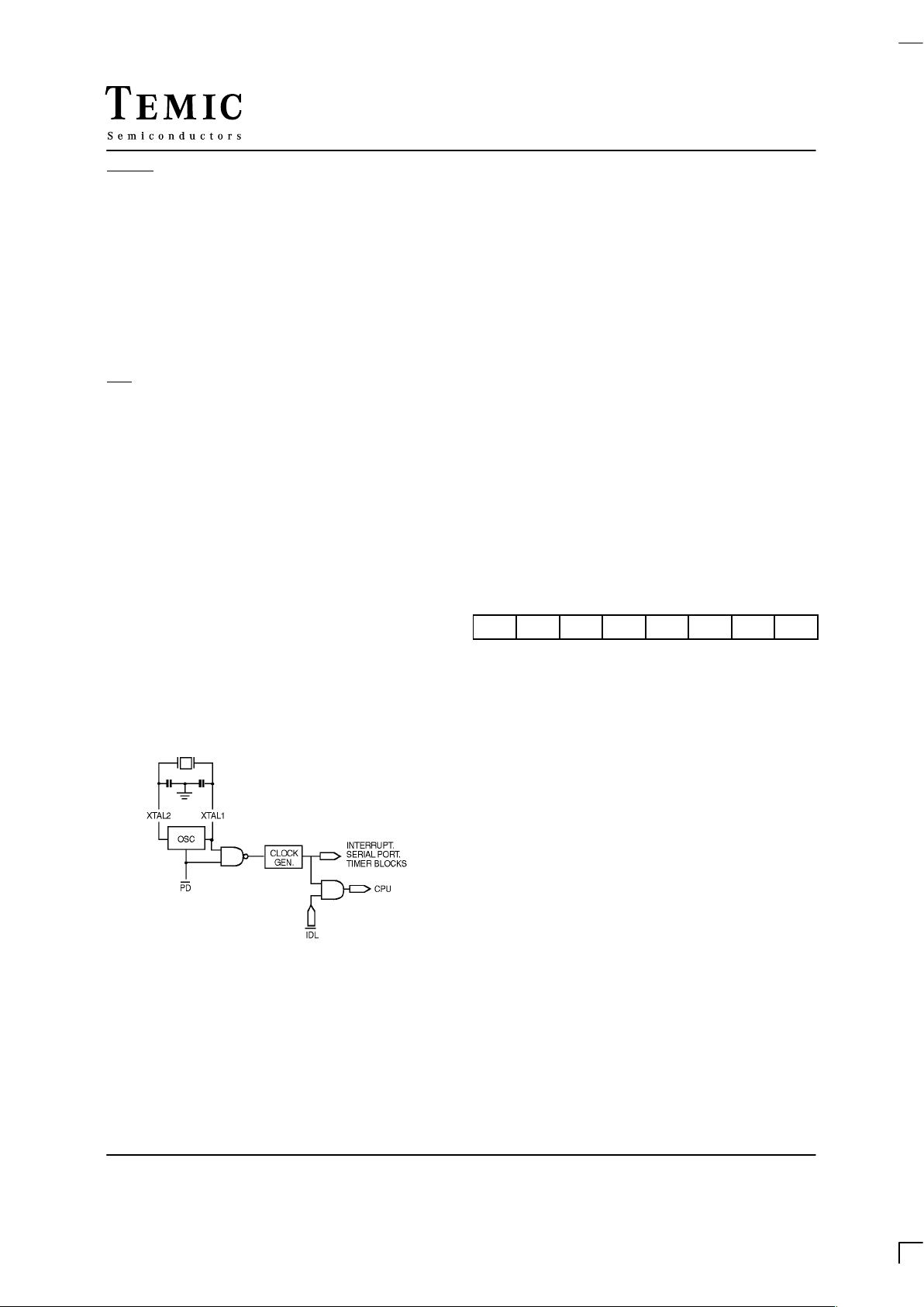
Idle And Power Down Operation
Figure 3. shows the internal Idle and Power Down clock
configuration. As illustrated, Power Down operation
stops the oscillator. Idle mode operation allows the
interrupt, serial port, and timer blocks to continue to
function, while the clock to the CPU is gated off.
These special modes are activated by software via the
Special Function Register, PCON. Its hardware address is
87H. PCON is not bit addressable.
Figure 3. Idle and Power Down Hardware.
PCON : Power Control Register
(MSB) (LSB)
SMOD – – – GF1 GF0 PD IDL
Symbol Position Name and Function
SMOD PCON.7 Double Baud rate bit. When set to
a 1, the baud rate is doubled when
the serial port is being used in
either modes 1, 2 or 3.
– PCON.6 (Reserved)
– PCON.5 (Reserved)
– PCON.4 (Reserved)
GF1 PCON.3 General-purpose flag bit.
GF0 PCON.2 General-purpose flag bit.
PD PCON.1 Power Down bit. Setting this bit
activates power down operation.
IDL PCON.0 Idle mode bit. Setting this bit
activates idle mode operation.
If 1’s are written to PD and IDL at the same time. PD
takes, precedence. The reset value of PCON is
(000X0000).
Idle Mode
The instruction that sets PCON.0 is the last instruction
executed before the Idle mode is activated. Once in the
Idle mode the CPU status is preserved in its entirety : the
Stack Pointer, Program Counter, Program Status Word,
Accumulator, RAM and all other registers maintain their
data during idle. Table 1 describes the status of the
external pins during Idle mode.
There are three ways to terminate the Idle mode.
Activation of any enabled interrupt will cause PCON.0 to
be cleared by hardware, terminating Idle mode. The
interrupt is serviced, and following RETI, the next
instruction to be executed will be the one following the
instruction that wrote 1 to PCON.0.
TSC80C31/80C51
Rev. E (14 Jan.97)
6
MATRA MHS
The flag bits GF0 and GF1 may be used to determine
whether the interrupt was received during normal
execution or during the Idle mode. For example, the
instruction that writes to PCON.0 can also set or clear one
or both flag bits. When Idle mode is terminated by an
enabled interrupt, the service routine can examine the
status of the flag bits.
The second way of terminating the Idle mode is with a
hardware reset. Since the oscillator is still running, the
hardware reset needs to be active for only 2 machine
cycles (24 oscillator periods) to complete the reset
operation.
Power Down Mode
The instruction that sets PCON.1 is the last executed prior
to entering power down. Once in power down, the
oscillator is stopped. The contents of the onchip RAM and
the Special Function Register is saved during power down
mode. The hardware reset initiates the Special Fucntion
Register. In the Power Down mode, VCC may be lowered
to mi-nimize circuit power consumption. Care must be
taken to ensure the voltage is not reduced until the power
down mode is entered, and that the voltage is restored
before the hardware reset is applied which freezes the
oscillator. Reset should not be released until the oscillator
has restarted and stabilized. A hardware reset is the only
way of exiting the power down mode.
Table 1 describes the status of the external pins while in
the power down mode. It should be noted that if the power
down mode is activated while in external program
memory, the port data that is held in the Special Function
Register P2 is restored to Port 2. If the data is a 1, the port
pin is held high during the power down mode by the
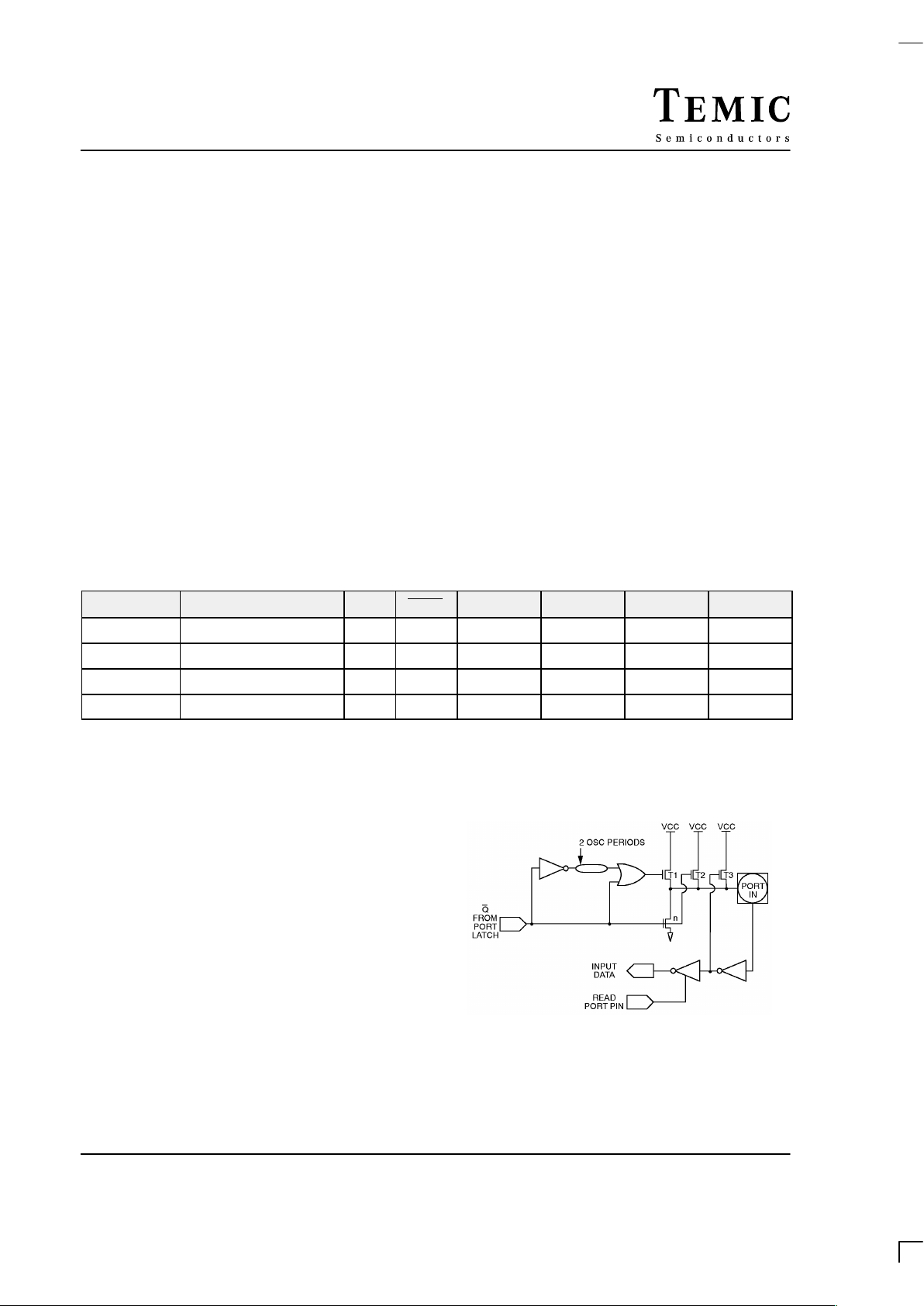
strong pullup, T1, shown in Figure 4.
Table 1. Status of the external pins during idle and power down modes.
MODE PROGRAM MEMORY ALE PSEN PORT0 PORT1 PORT2 PORT3
Idle Internal 1 1 Port Data Port Data Port Data Port Data
Idle External 1 1 Floating Port Data Address Port Data
Power Down Internal 0 0 Port Data Port Data Port Data Port Data
Power Down External 0 0 Floating Port Data Port Data Port Data
Stop Clock Mode
Due to static design, the TSC80C31/80C51 clock speed
can be reduced until 0 MHz without any data loss in
memory or registers. This mode allows step by step
utilization, and permits to reduce system power
consumption by bringing the clock frequency down to
any value. At 0 MHz, the power consumption is the same
as in the Power Down Mode.
I/O Ports
The I/O buffers for Ports 1, 2 and 3 are implemented as
shown in Figure 4.
Figure 4. I/O Buffers in the TSC80C31/80C51 (Ports
1, 2, 3).
 Loading...