

TEMIC TSC80251-SK Datasheet

TSC80251G2D
8/16-bit Microcontroller with Serial Communication
Interfaces
1. Description
The TSC80251G2D products are derivatives of the
TEMIC Microcontroller family based on the 8/16-bit
C251 Architecture. This family of products is tailored
to 8/16-bit microcontroller applications requiring an
increased instruction throughput, a reduced operating
frequency or a larger addressable memory space. The
architecture can provide a significant code size reduction
when compiling C programs while fully preserving the
legacy of C51 assembly routines.
The TSC80251G2D derivatives are pin and software
compatible with standard 80C51/Fx/Rx/Rx+ with
extended on-chip data memory (1 Kbyte RAM) and up
the TSC83251G2D and TSC87251G2D provide on-chip
code memory: 32 Kbytes ROM and 32 Kbytes EPROM/
OTPROM respectively.
They provide transparent enhancements to Intel’s
8xC251Sx family with an additional Synchronous Serial
Link Controller (SSLC supporting I2C, µWire and SPI
protocols), a Keyboard interrupt interface, a dedicated
Baud RateGenerator for UART, and Power Management
features.
TSC80251G2D derivatives are optimized for speed and
for low power consumption on a wide voltage range.
to 256 Kbytes of external code and data. Additionally,
Note:
This Datasheet provides the technical description of the TSC80251G2D derivatives. For further information on the device usage, please request
the TSC80251 Programmer’s Guide and the TSC80251G1D Design Guide.
2. Typical Applications
● ISDN Terminals
● High-Speed Modems
● PABX (SOHO)
● Line Cards
● DVD ROM and Players
● Printers
● Plotters
● Scanners
● Banking Machines
● Barcode Readers
● Smart Cards Readers
● High-End Digital Monitors
● High-End Joysticks
Rev. A - May 7, 1999 1

TSC80251G2D
3. Features
● Pin and Software Compatibility with Standard 80C51
Products and 80C51Fx/Rx/Rx+
● Plug-In Replacement of Intel’s 8xC251Sx
● C251 core: Intel’s MCS
®
251 D-step Compliance
• 40-byte register file
• Registers accessible as Bytes, Words or Dwords
• Three-stage instruction pipeline
• 16-bit internal code fetch
● Enriched C51 Instruction Set
• 16-bit and 32-bit ALU
• Compare and conditional jump instructions
• Expanded set of move instructions
● Linear Addressing
● 1 Kbyte of On-Chip RAM
● External Memory Space (Code/Data) Programmable
from 64 Kbytes to 256 Kbytes
● TSC87251G2D: 32 Kbytes of On-Chip EPROM/
OTPROM
• SINGLE PULSE Programming Algorithm
● TSC83251G2D:32 Kbytes of On-Chip Masked ROM
● TSC80251G2D: ROMless Version
● Four 8-bit Parallel I/O Ports (Ports 0, 1, 2 and 3 of
the standard 80C51)
● Serial I/O Port: full duplex UART (80C51
compatible) with independent Baud Rate Generator
● SSLC: Synchronous Serial Link Controller
• I2C multi-master protocol
•µWire and SPI master and slave protocols
● Three 16-bit Timers/Counters (Timers 0, 1 and 2 of
the standard 80C51)
● EWC: Event and Waveform Controller
• Compatible with Intel’s Programmable Counter
Array (PCA)
• Common 16-bit timer/counter reference with four
possible clock sources (Fosc/4, Fosc/12, Timer 1
and external input)
• Five modules, each with four programmable
modes:
- 16-bit software timer/counter
- 16-bit timer/counter capture input and
software pulse measurement
- High-speed output and 16-bit software pulse
width modulation (PWM)
- 8-bit hardware PWM without overhead
• 16-bit watchdog timer/counter capability
● Secure 14-bit Hardware Watchdog Timer
● Power Management
• Power-On reset (integrated on the chip)
• Power-Off flag (cold and warm resets)
• Software programmable system clock
• Idle mode
• Power-Down mode
● Keyboard Interrupt Interface on Port 1
● Non Maskable Interrupt Input (NMI)
● Real-Time Wait States Inputs (WAIT#/AWAIT#)
● ONCE mode and full speed Real-Time In-Circuit
Emulation support (Third Party Vendors)
● High Speed Versions:
• 4.5 to 5.5 V
• 16 MHz and 24 MHz
• Typical operating current: 35 mA @ 24 MHz
24 mA @ 16 MHz
• Typical power-down current: 2 µA
● Low Voltage Version:
• 2.7 to 5.5 V
• 16 MHz
• Typical operating current: 11 mA @ 3V
• Typical power-down current: 1 µA
● Temperature Ranges:
• Commercial (0°Cto+70°C)
• Industrial (-40°Cto+85°C)
• Option: extended range (-55°C to +125°C)
● Packages:
• PDIL 40, PLCC 44 and VQFP 44
• CDIL 40 and CQPJ 44 with window
• Options: known good dice and ceramic packages
2 Rev. A - May 7, 1999
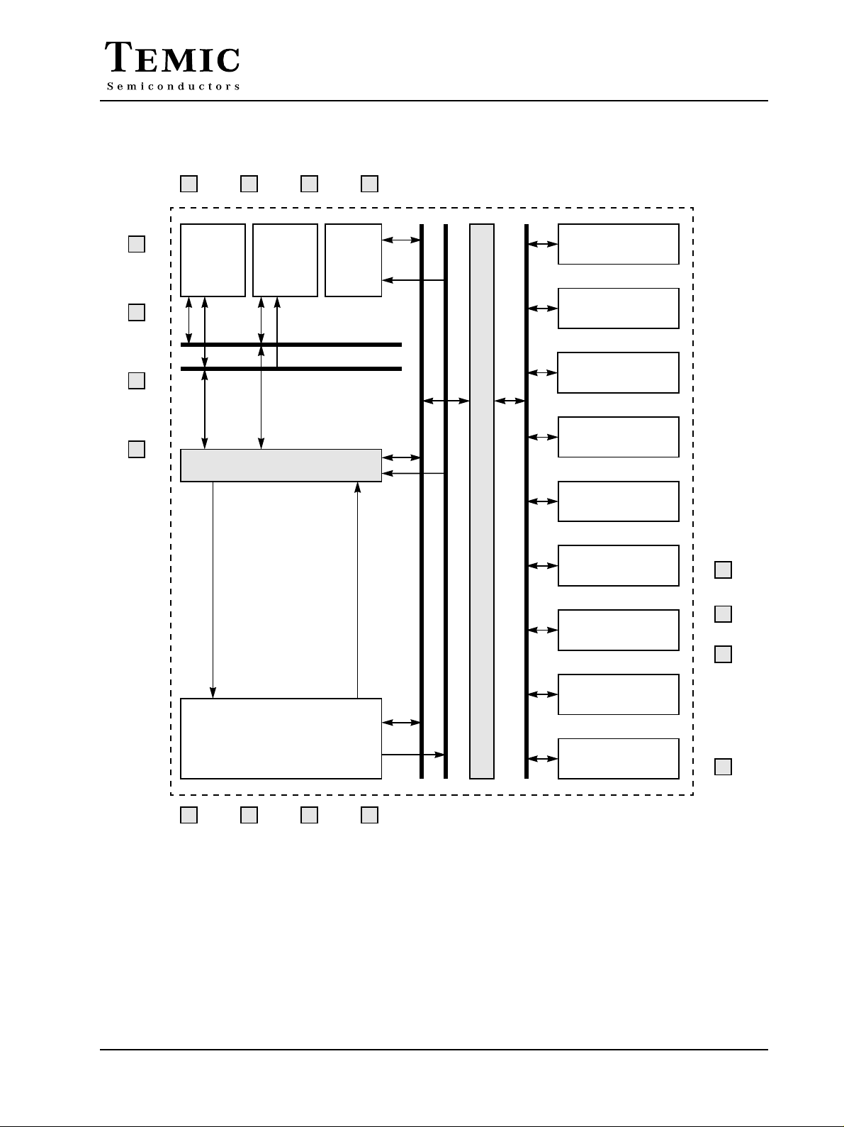
4. Block Diagram
P3(A16) P1(A17)P2(A15-8) P0(AD7-0)
PSEN#
PORTS 0-3
ALE/PROG#
EA#/VPP
AWAIT#
Bus Interface Unit
ROM
EPROM
OTPROM
32 Kbytes
16-bit Memory Code
16-bit Memory Address
RAM
1 Kbyte
TSC80251G2D
Timers 0, 1 and 2
UART
Baud Rate Generator
Event and Waveform
Controller
2
I
C/SPI/µWire
Controller
16-bit Instruction Bus
CPU
VDD VSS VSS1
Figure 1. TSC80251G2D Block Diagram
8-bit Data Bus
24-bit Program Counter Bus
VSS2
Peripheral Interface Unit
24-bit Data Address Bus
Watchdog Timer
Power Management
Clock System Prescaler
8-bit Internal Bus
Keyboard Interface
Interrupt Handler
RST
XTAL2
Clock Unit
XTAL1
NMI
Unit
Rev. A - May 7, 1999 3
TSC80251G2D
5. Pin Description
5.1 Pinout
P1.0/T2 VDD
P1.1/T2EX
P1.2/ECI
P1.3/CEX0
P1.4/CEX1/SS#
P1.6/CEX3/SCL/SCK/WAIT#
P1.7/A17/CEX4/SDA/MOSI/WCLK
RST
P3.0/RXD
P3.1/TXD
P3.2/INT0#
P3.3/INT1#
P3.4/T0
P3.5/T1
P3.7/A16/RD#
XTAL2
XTAL1
VSS P2.0/A8
Figure 2. TSC80251G2D 40-pin DIP package
1
2
3
4
5
6
7
8
9
10
11
12
13
14
15
16
17
18
19
20
TSC80251G2D
40
39
38
37
36
35P1.5/CEX2/MISO
34
33
32
31
30
29
28
27
26
25
24
23
22
21
P0.0/AD0
P0.1/AD1
P0.2/AD2
P0.3/AD3
P0.4/AD4
P0.5/AD5
P0.6/AD6
P0.7/AD7
EA#/VPP
ALE/PROG#
PSEN#
P2.7/A15
P2.6/A14
P2.5/A13
P2.4/A12P3.6/WR#
P2.3/A11
P2.2/A10
P2.1/A9
P1.4/CEX1/SS#
P1.3/CEX0
P1.2/ECI
P1.1/T2EX
P1.0/T2
VSS1
VDD
P0.0/AD0
P0.1/AD1
P0.2/AD2
P0.3/AD3
P1.5/CEX2/MISO
P1.6/CEX3/SCL/SCK/WAIT#
P1.7/A17/CEX4/SDA/MOSI/WCLK
RST
P3.0/RXD
AWAIT#
P3.1/TXD
P3.2/INT0#
P3.3/INT1#
P3.4/T0
P3.5/T1
65432
7
8
9
10
11
12
13
14
15
16
17
TSC80251G2D
1819202122232425262728
XTAL2
P3.6/WR#
P3.7/A16/RD#
XTAL1
VSS
1
VSS2
4443424140
P2.0/A8
P2.1/A9
P2.2/A10
P2.3/A11
39
38
37
36
35
34
33
32
31
30
29
P2.4/A12
P0.4/AD4
P0.5/AD5
P0.6/AD6
P0.7/AD7
EA#/VPP
NMI
ALE/PROG#
PSEN#
P2.7/A15
P2.6/A14
P2.5/A13
Figure 3. TSC80251G2D 44-pin PLCC Package
4 Rev. A - May 7, 1999
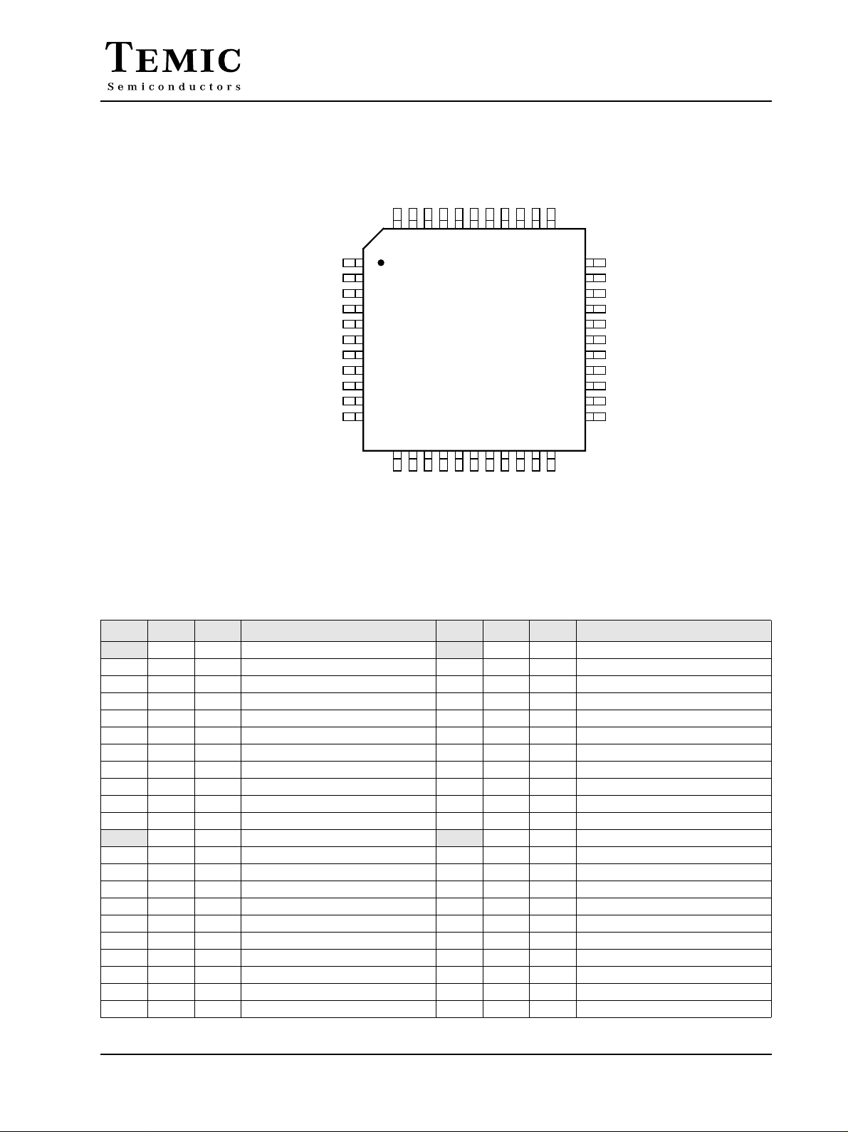
P1.5/CEX2/MISO
P1.6/CEX3/SCL/SCK/WAIT#
P1.7/A17/CEX4/SDA/MOSI/WCLK
RST
P3.0/RXD
AWAIT#
P3.1/TXD
P3.2/INT0#
P3.3/INT1#
P3.4/T0
P3.5/T1
Figure 4. TSC80251G2D 44-pin VQFP Package
P1.4/CEX1/SS#
P1.3/CEX0
P1.2/ECI
P1.1/T2EX
P1.0/T2
VSS1
4443424140393837363534
1
2
3
4
5
6
7
8
9
10
11
TSC80251G2D
1213141516171819202122
VSS
XTAL1
VSS2
XTAL2
P3.6/WR#
P3.7/A16/RD#
VDD
P0.0/AD0
P2.0/A8
P2.1/A9
TSC80251G2D
P0.1/AD1
P0.2/AD2
P0.3/AD3
33
P0.4/AD4
32
P0.5/AD5
31
P0.6/AD6
30
P0.7/AD7
29
EA#/VPP
28
NMI
27
ALE/PROG#
26
PSEN#
25
P2.7/A15
24
P2.6/A14
23
P2.5/A13
P2.2/A10
P2.3/A11
P2.4/A12
Table 1. TSC80251G2D Pin Assignment
DIP PLCC VQFP Name DIP PLCC VQFP Name
1 39 VSS1 23 17 VSS2
1 2 40 P1.0/T2 21 24 18 P2.0/A8
2 3 41 P1.1/T2EX 22 25 19 P2.1/A9
3 4 42 P1.2/ECI 23 26 20 P2.2/A10
4 5 43 P1.3/CEX0 24 27 21 P2.3/A11
5 6 44 P1.4/CEX1/SS# 25 28 22 P2.4/A12
6 7 1 P1.5/CEX2/MISO 26 29 23 P2.5/A13
7 8 2 P1.6/CEX3/SCL/SCK/WAIT# 27 30 24 P2.6/A14
8 9 3 P1.7/A17/CEX4/SDA/MOSI/WCLK 28 31 25 P2.7/A15
9 10 4 RST 29 32 26 PSEN#
10 11 5 P3.0/RXD 30 33 27 ALE/PROG#
12 6 AWAIT# 34 28 NMI
11 13 7 P3.1/TXD 31 35 29 EA#/VPP
12 14 8 P3.2/INT0# 32 36 30 P0.7/AD7
13 15 9 P3.3/INT1# 33 37 31 P0.6/AD6
14 16 10 P3.4/T0 34 38 32 P0.5/AD5
15 17 11 P3.5/T1 35 39 33 P0.4/AD4
16 18 12 P3.6/WR# 36 40 34 P0.3/AD3
17 19 13 P3.7/A16/RD# 37 41 35 P0.2/AD2
18 20 14 XTAL2 38 42 36 P0.1/AD1
19 21 15 XTAL1 39 43 37 P0.0/AD0
20 22 16 VSS 40 44 38 VDD
Rev. A - May 7, 1999 5
TSC80251G2D
5.2 Signals
Table 2. Product Name Signal Descriptions
Signal
Name
A17 O 18thAddress Bit
A16 O 17thAddress Bit
A15:8
AD7:0
ALE O Address Latch Enable
AWAIT# I Real-time Asynchronous Wait States Input
CEX4:0 I/O PCA Input/Output pins
EA# I External Access Enable
ECI O PCA External Clock input
MISO I/O SPI Master Input Slave Output line
MOSI I/O SPI Master Output Slave Input line
INT1:0# I External Interrupts 0 and 1
NMI I Non Maskable Interrupt
P0.0:7 I/O Port 0
Type Description
Output to memory as 18th external address bit (A17) in extended bus applications, depending
on the values of bits RD0 and RD1 in UCONFIG0 byte (see Table 13, Page 15).
Output to memory as 17th external address bit (A16) in extended bus applications, depending
on the values of bits RD0 and RD1 in UCONFIG0 byte (see Table 13, Page 15).
(1)
(1)
O Address Lines
Upper address lines for the external bus.
I/O Address/Data Lines
Multiplexed lower address lines and data for the external memory.
ALE signals the start of an external bus cycle and indicates that valid address information
are available on lines A16/A17 and A7:0. An external latch can use ALE to demultiplex the
address from address/data bus.
When this pin is active (low level), the memory cycle is stretched until it becomes high.
When using the Product Name as a pin-for-pin replacement for a 8xC51 product, AWAIT#
can be unconnected without loss of compatibility or power consumption increase (on-chip
pull-up).
Not available on DIP package.
CEXx are input signals for the PCA capture mode and output signals for the PCA compare
and PWM modes.
EA# directs program memory accesses to on-chip or off-chip code memory.
For EA#= 0, all program memory accesses are off-chip.
For EA#= 1, an access is on-chip ROM if the address is within the range of the on-chip
ROM; otherwise the access is off-chip. The value of EA# is latched at reset.
For devices without ROM on-chip, EA# must be strapped to ground.
ECI is the external clock input to the 16-bit PCA timer.
When SPI is in master mode, MISO receives data from the slave peripheral. When SPI is in
slave mode, MISO outputs data to the master controller.
When SPI is in master mode, MOSI outputs data to the slave peripheral. When SPI is in
slave mode, MOSI receives data from the master controller.
INT1#/INT0# inputs set IE1:0 in the TCON register. If bits IT1:0 in the TCON register are
set, bits IE1:0 are set by a falling edge on INT1#/INT0#. If bits IT1:0 are cleared, bits IE1:0
are set by a low level on INT1#/INT0#.
Holding this pin high for 24 oscillator periods triggers an interrupt.
When using the Product Name as a pin-for-pin replacement for a 8xC51 product, NMI can
be unconnected without loss of compatibility or power consumption increase (on-chip pulldown).
Not available on DIP package.
P0 is an 8-bit open-drain bidirectional I/O port. Port 0 pins that have 1s written to them float
and can be used as high impedance inputs. To avoid any paraitic current consumption, Floating
P0 inputs must be polarized to VDDor VSS.
Alternate
Function
P1.7
P3.7
P2.7:0
P0.7:0
P1.7:3
P1.2
P1.5
P1.7
P3.3:2
AD7:0
6 Rev. A - May 7, 1999

TSC80251G2D
Signal
Name
P1.0:7 I/O Port 1
P2.0:7 I/O Port 2
P3.0:7 I/O Port 3
PROG# I Programming Pulse input
PSEN# O Program Store Enable/Read signal output
RD# O Read or 17thAddress Bit (A16)
RST I Reset input to the chip
RXD I/O Receive Serial Data
SCL I/O I2C Serial Clock
SCK I/O SPI Serial Clock
SDA I/O I2C Serial Data
SS# I SPI Slave Select Input
T1:0 I/O Timer 1:0 External Clock Inputs
T2 I/O Timer 2 Clock Input/Output
T2EX I Timer 2 External Input
TXD O Transmit Serial Data
VDD PWR Digital Supply Voltage
VPP I Programming Supply Voltage
Type Description
P1 is an 8-bit bidirectional I/O port with internal pull-ups. P1 provides interrupt capability
for a keyboard interface.
P2 is an 8-bit bidirectional I/O port with internal pull-ups.
P3 is an 8-bit bidirectional I/O port with internal pull-ups.
The programming pulse is applied to this input for programming the on-chip EPROM/
OTPROM.
PSEN# is asserted for a memory address range that depends on bits RD0 and RD1 in
UCONFIG0 byte (see Table 13, Page 15).
Read signal output to external data memory depending on the values of bits RD0 and RD1
in UCONFIG0 byte (see Table 13, Page 15).
Holding this pin high for 64 oscillator periods while the oscillator is running resets the device.
The Port pins are driven to their reset conditions when a voltage greater than V
whether or not the oscillator is running.
This pin has an internal pull-down resistor which allows the device to be reset by connecting
a capacitor between this pin and VDD.
Asserting RST when the chip is in Idle mode or Power-Down mode returns the chip to normal
operation.
RXD sends and receives data in serial I/O mode 0 and receives data in serial I/O modes 1,
2 and 3.
When I2C controller is in master mode, SCL outputs the serial clock to slave peripherals.
When I2C controller is in slave mode, SCL receives clock from the master controller.
When SPI is in master mode, SCK outputs clock to the slave peripheral. When SPI is in
slave mode, SCK receives clock from the master controller.
SDA is the bidirectional I2C data line.
When in Slave mode, SS# enables the slave mode.
When timer 1:0 operates as a counter, a falling edge on the T1:0 pin increments the count.
For the timer 2 capture mode, T2 is the external clock input. For the Timer 2 clock-out mode,
T2 is the clock output.
In timer 2 capture mode, a falling edge initiates a capture of the timer 2 registers. In autoreload mode, a falling edge causes the timer 2 register to be reloaded. In the up-down counter
mode, this signal determines the count direction: 1= up, 0= down.
TXD outputs the shift clock in serial I/O mode 0 and transmits data in serial I/O modes 1,
2 and 3.
Connect this pin to +5V or +3V supply voltage.
The programming supply voltage is applied to this input for programming the on-chip EPROM/
OTPROM.
is applied,
IH1
Alternate
Function
A15:8
P3.7
P3.0
P1.6
P1.6
P1.7
P1.4
P1.0
P1.1
P3.1
Rev. A - May 7, 1999 7
TSC80251G2D
Signal
Name
VSS GND Circuit Ground
VSS1 GND Secondary Ground 1
VSS2 GND Secondary Ground 2
WAIT# I Real-time Synchronous Wait States Input
WCLK O Wait Clock Output
WR# O Write
XTAL1 I Input to the on-chip inverting oscillator amplifier
XTAL2 O Output of the on-chip inverting oscillator amplifier
Note:
1. The description of A15:8/P2.7:0 and AD7:0/P0.7:0 are for the Non-Page mode chip configuration. If the chip is configured in Page mode
operation, port 0 carries the lower address bits (A7:0) while port 2 carries the upper address bits (A15:8) and the data (D7:0).
Type Description
Connect this pin to ground.
This ground is provided to reduce ground bounce and improve power supply bypassing.
Connection of this pin to ground is recommended. However, when using the TSC80251G2D
as a pin-for-pin replacement for a 8xC51 product, VSS1 can be unconnected without loss of
compatibility.
Not available on DIP package.
This ground is provided to reduce ground bounce and improve power supply bypassing.
Connection of this pin to ground is recommended. However, when using the TSC80251G2D
as a pin-for-pin replacement for a 8xC51 product, VSS2 can be unconnected without loss of
compatibility.
Not available on DIP package.
The real-time WAIT# input is enabled by setting RTWE bit in WCON (S:A7h). During bus
cycles, the external memory system can signal ‘system ready’ to the microcontroller in real
time by controlling the WAIT# input signal.
The real-time WCLK output is enabled by setting RTWCE bit in WCON (S:A7h). When
enabled, the WCLK output produces a square wave signal with a period of one half the
oscillator frequency.
Write signal output to external memory.
To use the internal oscillator, a crystal/resonator circuit is connected to this pin. If an external
oscillator is used, its output is connected to this pin. XTAL1 is the clock source for internal
timing.
To use the internal oscillator, a crystal/resonator circuit is connected to this pin. If an external
oscillator is used, leave XTAL2 unconnected.
Alternate
Function
P1.6
P1.7
P3.6
8 Rev. A - May 7, 1999
TSC80251G2D
6. Address Spaces
The TSC80251G2D derivatives implement four different address spaces:
● On-chip ROM program/code memory (not present in ROMless devices)
● On-chip RAM data memory
● Special Function Registers (SFRs)
● Configuration array
6.1 Program/Code Memory
The TSC83251G2D and TSC87251G2D implement 32 Kbytes of on-chip program/code memory. Figure 5 shows
the split of the internal and external program/code memory spaces. If EA# is tied to a high level, the 32-Kbyte
on-chip program memory is mapped in the lower part of segment FF: where the C251 core jumps after reset. The
rest of the program/code memory space is mapped to the external memory. If EA# is tied to a low level, the
internal program/code memory is not used and all the accesses are directed to the external memory.
The TSC83251G2D products provide the internal program/code memory in a masked ROM memory while the
TSC87251G2D products provide it in an EPROM memory. For the TSC80251G2D products, there is no internal
program/code memory and EA# must be tied to a low level.
32 Kbytes
32 Kbytes
64 Kbytes
128 Kbytes
Program/code
External Memory Space
Program/code
Segments
FF:FFFFh
FF:8000h
FF:7FFFh
FF:0000h
FE:FFFFh
FE:0000h
FD:FFFFh
Reserved
02:0000h
01:FFFFh
01:0000h
00:FFFFh
00:0000h
On-chip ROM/EPROM
Code Memory
32 KbytesEA#= 0 EA#= 1
Figure 5. Program/Code Memory Mapping
Notes:
Special care should be taken when the Program Counter (PC) increments:
1. If the program executes exclusively from on-chip code memory (not from external memory), beware of executing code from the upper eight
bytes of the on-chip ROM (FF:7FF8h-FF:7FFFh). Because of its pipeline capability, the TSC80251G2D derivative may attempt to prefetch
code from external memory (at an address above FF:7FFFh) and thereby disrupt I/O Ports 0 and 2. Fetching code constants from these
8 bytes does not affect Ports 0 and 2.
2. When PC reaches the end of segment FF:, it loops to the reset address FF:0000h (for compatibility with the C51 Architecture). When PC
increments beyond the end of segment FE:, it continues at the reset address FF:0000h (linearity). When PC increments beyond the end of
segment 01:, it loops to the beginning of segment 00: (this prevents from its going into the reserved area).
Rev. A - May 7, 1999 9
TSC80251G2D
6.2 Data Memory
The TSC80251G2D derivatives implement 1 Kbyte of on-chip data RAM. Figure 6 shows the split of the internal
and external data memory spaces. This memory is mapped in the data space just over the 32 bytes of registers
area (see TSC80251 Programmers’ Guide). Hence, the part of the on-chip RAM located from 20h to FFh is bit
addressable. This on-chip RAM is not accessible through the program/code memory space.
For faster computation with the on-chip ROM/EPROM code of the TSC83251G2D/TSC87251G2D, its upper 16
Kbytes are also mapped in the upper part of the region 00: if the On-Chip Code Memory Map configuration bit
is cleared (EMAP# bit in UCONFIG1 byte, see Figure 8). However, if EA# is tied to a low level, the TSC80251G2D
derivative is running as a ROMless product and the code is actually fetched in the corresponding external memory
(i.e. the upper 16 Kbytes of the lower 32 Kbytes of the segment FF:). If EMAP# bit is set, the on-chip ROM is
not accessible through the region 00:.
All the accesses to the portion of the data space with no on-chip memory mapped onto are redirected to the external
memory.
Data External
Memory Space
On-chip ROM/EPROM
Code MemoryData Segments
32 Kbytes
32 Kbytes
64 Kbytes
64 Kbytes
16 Kbytes
≈47 Kbytes
FF:FFFFh
FF:8000h
FF:7FFFh
EA#= 0 EA#= 1
EMAP#= 1
FF:0000h
FE:FFFFh
FE:0000h
FD:FFFFh
Reserved
02:0000h
01:FFFFh
01:0000h
00:FFFFh
00:C000h
00:BFFFh
00:0420h
EMAP#= 0
Figure 6. Data Memory Mapping
16 Kbytes
16 Kbytes
RAM Data
1 Kbyte
32 bytes reg.
6.3 Special Function Registers
The Special Function Registers (SFRs) of the TSC80251G2D derivatives fall into the categories detailed in Table 3
to Table 11.
SFRs are placed in a reserved on-chip memory region S: which is not represented in the data memory mapping
(Figure 6). The relative addresses within S: of these SFRs are provided together with their reset values in Table 12.
They are upward compatible with the SFRs of the standard 80C51 and the Intel’s 80C251Sx family. In this table,
the C251 core registers are identified by Note 1 and are described in the TSC80251 Programmer’s Guide. The
other SFRs are described in the TSC80251G1D Design Guide. All the SFRs are bit-addressable using the C251
instruction set.
10 Rev. A - May 7, 1999
TSC80251G2D
Table 3. C251 Core SFRs
Mnemonic Name Mnemonic Name
(1)
ACC
(1)
B
PSW Program Status Word DPH
PSW1 Program Status Word 1 DPXL
(1)
SP
Note:
1. These SFRs can also be accessed by their corresponding registers in the register file.
Accumulator SPH
B Register DPL
Stack Pointer - LSB of SPX
Table 4. I/O Port SFRs
Mnemonic Name Mnemonic Name
P0 Port 0 P2 Port 2
P1 Port 1 P3 Port 3
Table 5. Timers SFRs
Mnemonic Name Mnemonic Name
TL0 Timer/Counter 0 Low Byte TMOD Timer/Counter 0 and 1 Modes
TH0 Timer/Counter 0 High Byte T2CON Timer/Counter 2 Control
TL1 Timer/Counter 1 Low Byte T2MOD Timer/Counter 2 Mode
TH1 Timer/Counter 1 High Byte RCAP2L Timer/Counter 2 Reload/Capture Low Byte
TL2 Timer/Counter 2 Low Byte RCAP2H Timer/Counter 2 Reload/Capture High Byte
TH2 Timer/Counter 2 High Byte WDTRST WatchDog Timer Reset
TCON Timer/Counter 0 and 1 Control
(1)
(1)
(1)
(1)
Stack Pointer High - MSB of SPX
Data Pointer Low byte - LSB of DPTR
Data Pointer High byte - MSB of DPTR
Data Pointer Extended Low byte of DPX - Region
number
Table 6. Serial I/O Port SFRs
Mnemonic Name Mnemonic Name
SCON Serial Control SADDR Slave Address
SBUF Serial Data Buffer BRL Baud Rate Reload
SADEN Slave Address Mask BDRCON Baud Rate Control
Table 7. SSLC SFRs
Mnemonic Name Mnemonic Name
SSCON Synchronous Serial control SSADR Synchronous Serial Address
SSDAT Synchronous Serial Data SSBR Synchronous Serial Bit Rate
SSCS Synchronous Serial Control and Status
Rev. A - May 7, 1999 11
TSC80251G2D
Table 8. Event Waveform Control SFRs
Mnemonic Name Mnemonic Name
CCON EWC-PCA Timer/Counter Control CCAP0L EWC-PCA Compare Capture Module 0 Low Register
CMOD EWC-PCA Timer/Counter Mode CCAP1L EWC-PCA Compare Capture Module 1 Low Register
CL EWC-PCA Timer/Counter Low Register CCAP2L EWC-PCA Compare Capture Module 2 Low Register
CH EWC-PCA Timer/Counter High Register CCAP3L EWC-PCA Compare Capture Module 3 Low Register
CCAPM0 EWC-PCA Timer/Counter Mode 0 CCAP4L EWC-PCA Compare Capture Module 4 Low Register
CCAPM1 EWC-PCA Timer/Counter Mode 1 CCAP0H EWC-PCA Compare Capture Module 0 High Register
CCAPM2 EWC-PCA Timer/Counter Mode 2 CCAP1H EWC-PCA Compare Capture Module 1 High Register
CCAPM3 EWC-PCA Timer/Counter Mode 3 CCAP2H EWC-PCA Compare Capture Module 2 High Register
CCAPM4 EWC-PCA Timer/Counter Mode 4 CCAP3H EWC-PCA Compare Capture Module 3 High Register
CCAP4H EWC-PCA Compare Capture Module 4 High Register
Table 9. System Management SFRs
Mnemonic Name Mnemonic Name
PCON Power Control CKRL Clock Reload
POWM Power Management WCON Synchronous Real-Time Wait State Control
Table 10. Interrupt SFRs
Mnemonic Name Mnemonic Name
IE0 Interrupt Enable Control 0 IPL0 Interrupt Priority Control Low 0
IE1 Interrupt Enable Control 1 IPH1 Interrupt Priority Control High 1
IPH0 Interrupt Priority Control High 0 IPL1 Interrupt Priority Control Low 1
Table 11. Keyboard Interface SFRs
Mnemonic Name Mnemonic Name
P1IE Port 1 Input Interrupt Enable P1LS Port 1 Level Selection
P1F Port 1 Flag
12 Rev. A - May 7, 1999

TSC80251G2D
Table 12. SFR Addresses and Reset Values
0/8 1/9 2/A 3/B 4/C 5/D 6/E 7/F
F8h
(1)
F0h
E8h
E0h
D8h
D0h
C8h
C0h C7h
B8h
B0h
A8h
A0h
98h
90h
88h
80h
B
0000 0000
(1)
ACC
0000 0000
CCON
00X0 0000
(1)
PSW
0000 0000
T2CON
0000 0000
IPL0
X000 0000
P3
1111 1111
IE0
0000 0000
P2
1111 1111
SCON
0000 0000
P1
1111 1111
TCON
0000 0000
P0
1111 1111
0/8 1/9 2/A 3/B 4/C 5/D 6/E 7/F
CH
0000 0000
CL
0000 0000
CMOD
00XX X000
(1)
PSW1
0000 0000
T2MOD
XXXX XX00
SADEN
0000 0000
IE1
XX0X XXX0
SADDR
0000 0000
SBUF
XXXX XXXX
TMOD
0000 0000
(1)
SP
0000 0111
CCAP0H
0000 0000
CCAP0L
0000 0000
CCAPM0
X000 0000
RCAP2L
0000 0000
IPL1
XX0X XXX0
BRL
0000 0000
SSBR
0000 0000
TL0
0000 0000
(1)
DPL
0000 0000
CCAP1H
0000 0000
CCAP1L
0000 0000
CCAPM1
X000 0000
RCAP2H
0000 0000
IPH1
XX0X XXX0
BDRCON
XXX0 0000
SSCON
(2)
TL1
0000 0000
(1)
DPH
0000 0000
CCAP2H
0000 0000
CCAP2L
0000 0000
CCAPM2
X000 0000
TL2
0000 0000
P1LS
0000 0000
SSCS
(3)
TH0
0000 0000
(1)
DPXL
0000 0001
CCAP3H
0000 0000
CCAP3L
0000 0000
CCAPM3
X000 0000
TH2
0000 0000
P1IE
0000 0000
SSDAT
0000 0000
TH1
0000 0000
CCAP4H
0000 0000
CCAP4L
0000 0000
CCAPM4
X000 0000
(1)
SPH
0000 0000
WDTRST
1111 1111
P1F
0000 0000
SSADR
0000 0000
CKRL
0000 1000
IPH0
X000 0000
WCON
XXXX XX00
POWM
0XXX XXXX
PCON
0000 0000
FFh
F7h
EFh
E7h
DFh
D7h
CFh
BFh
B7h
AFh
A7h
9Fh
97h
8Fh
87h
Reserved
Notes:
1. These registers are described in the TSC80251 Programmer’s Guide (C251 core registers).
2. In I2C and SPI modes, SSCON is splitted in two separate registers. SSCON reset value is 0000 0000 in I2C mode and 0000 0100 in SPI mode.
3. In read and write modes, SSCS is splitted in two separate registers. SSCS reset value is 1111 1000 in read mode and 0000 0000 in write mode.
Rev. A - May 7, 1999 13
TSC80251G2D
6.4 Configuration Bytes
The TSC80251G2D derivatives provide user design flexibility by configuring certain operating features at device
reset. These features fall into the following categories:
• external memory interface (Page mode, address bits, programmed wait states and the address range for RD#,
WR#, and PSEN#)
• source mode/binary mode opcodes
• selection of bytes stored on the stack by an interrupt
• mapping of the upper portion of on-chip code memory to region 00:
Two user configuration bytes UCONFIG0 (see Figure 7) and UCONFIG1 (see Figure 8) provide the information.
When EA# is tied to a low level, the configuration bytes are fetched from the external address space. The
TSC80251G2D derivatives reserve the top eight bytes of the memory address space (FF:FFF8h-FF:FFFFh) for an
external 8-byte configuration array. Only two bytes are actually used: UCONFIG0 at FF:FFF8h and UCONFIG1
at FF:FFF9h.
For the mask ROM devices, configuration information is stored in on-chip memory (see ROM Verifying). When
EA# is tied to a high level, the configuration information is retrieved from the on-chip memory instead of the
external address space and there is no restriction in the usage of the external memory.
UCONFIG0
Configuration Byte 0
76543210
- WSA1# WSA0# XALE# RD1 RD0 PAGE# SRC
Bit Number Bit Mnemonic Description
7-
6 WSA1#
5 WSA0#
4 XALE#
3 RD1
2 RD0
1 PAGE#
0 SRC
Reserved
Set this bit when writing to UCONFIG0.
Wait State A bits
Select the number of wait states for RD#, WR# and PSEN# signals for external memory accesses
(all regions except 01:).
WSA1# WSA0# Number of Wait States
00 3
01 2
10 1
11 0
Extend ALE bit
Clear to extend the duration of the ALE pulse from T
Set to minimize the duration of the ALE pulse to 1·T
Memory Signal Select bits
Specify a 18-bit, 17-bit or 16-bit external address bus and the usage of RD#, WR# and PSEN#
signals (see Table 13).
Page Mode Select bit
Clear to select the faster Page mode with A15:8/D7:0 on Port 2 and A7:0 on Port 0.
Set to select the non-Page mode
Source Mode/Binary Mode Select bit
Clear to select the binary mode.
Set to select the source mode.
(1)
(2)
with A15:8 on Port 2 and A7:0/D7:0 on Port 0.
OSC
OSC
to 3·T
.
OSC.
Notes:
1. UCONFIG0 is fetched twice so it can be properly read both in Page or Non-Page modes. If P2.1 is cleared during the first data fetch, a
Page mode configuration is used, otherwise the subsequent fetches are performed in Non-Page mode.
2. This selection provides compatibility with the standard 80C51 hardware which is multiplexing the address LSB and the data on Port 0.
Figure 7. Configuration Byte 0
14 Rev. A - May 7, 1999
TSC80251G2D
UCONFIG1
Configuration Byte 1
76543210
CSIZE - - INTR WSB WSB1# WSB0# EMAP#
Bit Number Bit Mnemonic Description
CSIZE
TSC87251G2D
7
6-
5-
4 INTR
3 WSB
2 WSB1#
1 WSB0#
0 EMAP#
Notes:
1. The CSIZE is only available on EPROM/OTPROM products.
2. Two or four bytes are transparently popped according to INTR when using the RETI instruction. INTR must be set if interrupts are used
with code executing outside region FF:.
3. Use only for Step A compatibility; set this bit when WSB1:0# are used.
TSC80251G2D
TSC83251G2D
On-Chip Code Memory Size bit
Clear to select 16 Kbytes of on-chip code memory (TSC87251G1D product).
Set to select 32 Kbytes of on-chip code memory (TSC87251G2D product).
Reserved
Set this bit when writing to UCONFIG1.
Reserved
Set this bit when writing to UCONFIG1.
Reserved
Set this bit when writing to UCONFIG1.
Interrupt Mode bit
Clear so that the interrupts push two bytes onto the stack (the two lower bytes of the PC register).
Set so that the interrupts push four bytes onto the stack (the three bytes of the PC register and the
PSW1 register).
Wait State B bit
Clear to generate one wait state for memory region 01:.
Set for no wait states for memory region 01:.
Wait State B bits
Select the number of wait states for RD#, WR# and PSEN# signals for external memory accesses
(only region 01:).
WSB1# WSB0# Number of Wait States
00 3
01 2
10 1
11 0
On-Chip Code Memory Map bit
Clear to map the upper 16 Kbytes of on-chip code memory (at FF:4000h-FF:7FFFh) to the data
space (at 00:C000h-00:FFFFh).
Set not to map the upper 16 Kbytes of on-chip code memory (at FF:4000h-FF:7FFFh) to the data
space.
(2)
(3)
Figure 8. Configuration Byte 1
(1)
Table 13. Address Ranges and Usage of RD#, WR# and PSEN# Signals
RD1 RD0 P1.7 P3.7/RD# PSEN# WR# External Memory
0 0 A17 A16
0 1 I/O pin A16
1 0 I/O pin I/O pin
1 1 I/O pin
Note:
1. This selection provides compatibility with the standard 80C51 hardware which has separate external memory spaces for data and code.
Read signal for regions 00:
and 01:
Read signal for all external
memory locations
Read signal for all external
memory locations
Read signal for all external
memory locations
Read signal for regions FE:
and FF:
Write signal for all external
memory locations
Write signal for all external
memory locations
Write signal for all external
memory locations
Write signal for all external
memory locations
256 Kbytes
128 Kbytes
64 Kbytes
2 × 64 Kbytes
(1)
Rev. A - May 7, 1999 15
TSC80251G2D
7. Instruction Set Summary
This section contains tables that summarize the instruction set. For each instruction there is a short description, its
length in bytes, and its execution time in states (one state time is equal to two system clock cycles). There are
two concurrent processes limiting the effective instruction throughput:
● Instruction Fetch
● Instruction Execution
Table 20 to Table 34 assume code executing from on-chip memory, then the CPU is fetching 16-bit at a time and
this is never limiting the execution speed.
If the code is fetched from external memory, a pre-fetch queue will store instructions ahead of execution to optimize
the memory bandwidth usage when slower instructions are executed. However, the effective speed may be limited
depending on the average size of instructions (for the considered section of the program flow). The maximum
average instruction throughput is provided by Table 14 depending on the external memory configuration (from
Page Mode to Non-Page Mode and the maximum number of wait states). If the average size of instructions is not
an integer, the maximum effective throughput is found by pondering the number of states for the neighbor integer
values.
Table 14. Minimum Number of States per Instruction for given Average Sizes
Average size of
Instructions
(bytes)
1123456
224681012
3 3 6 9 12 15 18
4 4 8 12162024
5 5 10 15 20 25 30
Page Mode
(states)
0 Wait State 1 Wait State 2 Wait States 3 Wait States 4 Wait States
Non-Page Mode (states)
If the average execution time of the considered instructions is larger than the number of states given by Table 14,
this larger value will prevail as the limiting factor. Otherwise, the value from Table 14 must be taken. This is
providing a fair estimation of the execution speed but only the actual code execution can provide the final value.
7.1 Notation for Instruction Operands
Table 15 to Table 19 provide notation for Instruction Operands.
Table 15. Notation for Direct Addressing
Direct Address Description C251 C51
dir8
dir16 A 16-bit memory address (00:0000h-00:FFFFh) used in direct addressing. ✓
A direct 8-bit address. This can be a memory address (00h-7Fh) or a SFR address (80hFFh). It is a byte (default), word or double word depending on the other operand.
Table 16. Notation for Immediate Addressing
✓✓
Immediate
Address
#data An 8-bit constant that is immediately addressed in an instruction ✓✓
#data16 A 16-bit constant that is immediately addressed in an instruction ✓
#0data16
#1data16
#short A constant, equal to 1, 2, or 4, that is immediately addressed in an instruction. ✓
A 32-bit constant that is immediately addressed in an instruction. The upper word is filled
with zeros (#0data16) or ones (#1data16).
Description C251 C51
✓
Rev. A - May 7, 1999 16
TSC80251G2D
Table 17. Notation for Bit Addressing
Direct Address Description C251 C51
A directly addressed bit (bit number= 00h-FFh) in memory or an SFR. Bits 00h-7Fh are
bit51
bit A directly addressed bit in memory locations 00:0020h-00:007Fh or in any defined SFR. ✓
Direct Address Description C251 C51
rel
addr11
addr16
addr24 A 24-bit target address. The target can be anywhere within the 16-Mbyte address space. ✓
Register Description C251 C51
@Ri A memory location (00h-FFh) addressed indirectly via byte registers R0 or R1 ✓
Rn
n
Rm
Rmd
Rms
m, md, ms
WRj
WRjd
WRjs
@WRj
@WRj +dis16
j, jd, js
DRk
DRkd
DRks
@DRk
@DRk +dis16
k, kd, ks
the 128 bits in byte locations 20h-2Fh in the on-chip RAM. Bits 80h-FFh are the 128 bits
in the 16 SFRs with addresses that end in 0h or 8h, S:80h, S:88h, S:90h,..., S:F0h, S:F8h.
Table 18. Notation for Destination in Control Instructions
A signed (two’s complement) 8-bit relative address. The destination is -128 to +127 bytes
relative to the next instruction’s first byte.
An 11-bit target address. The target is in the same 2-Kbyte block of memory as the next
instruction’s first byte.
A 16-bit target address. The target can be anywhere within the same 64-Kbyte region as
the next instruction’s first byte.
Table 19. Notation for Register Operands
Byte register R0-R7 of the currently selected register bank
Byte register index: n= 0-7
Byte register R0-R15 of the currently selected register file
Destination register
Source register
Byte register index: m, md, ms= 0-15
Word register WR0, WR2, ..., WR30 of the currently selected register file
Destination register
Source register
A memory location (00:0000h-00:FFFFh) addressed indirectly through word register WR0WR30, is the target address for jump instructions.
A memory location (00:0000h-00:FFFFh) addressed indirectly through word register (WR0WR30) + 16-bit signed (two’s complement) displacement value
Word register index: j, jd, js= 0-30
Dword register DR0, DR4, ..., DR28, DR56, DR60 of the currently selected register file
Destination register
Source register
A memory location (00:0000h-FF:FFFFh) addressed indirectly through dword register DR0DR28, DR56 and DR60, is the target address for jump instruction
A memory location (00:0000h-FF:FFFFh) addressed indirectly through dword register (DR0DR28, DR56, DR60) + 16-bit (two’s complement) signed displacement value
Dword register index: k, kd, ks= 0, 4, 8..., 28, 56, 60
✓✓
✓
✓
✓
✓
✓
✓
✓
17 Rev. A - May 7, 1999
TSC80251G2D
7.2 Size and Execution Time for Instruction Families
Table 20. Summary of Add and Subtract Instructions
Add ADD <dest>, <src> dest opnd ← dest opnd + src opnd
Subtract SUB <dest>, <src> dest opnd ← dest opnd - src opnd
Add with Carry ADDC <dest>, <src> (A) ← (A) + src opnd + (CY)
Subtract with Borrow SUBB <dest>, <src> (A) ← (A) - src opnd - (CY)
Mnemonic <dest>, <src>
A, Rn Register to ACC 1 1 2 2
ADD
ADD / SUB
ADDC / SUBB
Notes:
1. A shaded cell denotes an instruction in the C51 Architecture.
2. If this instruction addresses an I/O Port (Px, x= 0-3), add 1 to the number of states. Add 2 if it addresses a Peripheral SFR.
3. If this instruction addresses external memory location, add N+2 to the number of states (N: number of wait states).
4. If this instruction addresses external memory location, add 2(N+2) to the number of states (N: number of wait states).
A, dir8 Direct address to ACC 2 1
A, @Ri Indirect address to ACC 1 2 2 3
A, #data Immediate data to ACC 2 1 2 1
Rmd, Rms Byte register to/from byte register 3 2 2 1
WRjd, WRjs Word register to/from word register 3 3 2 2
DRkd, DRks Dword register to/from dword register 3 5 2 4
Rm, #data Immediate 8-bit data to/from byte register 4 3 3 2
WRj, #data16 Immediate 16-bit data to/from word register 5 4 4 3
DRk, #0data16 16-bit unsigned immediate data to/from dword register 5 6 4 5
Rm, dir8 Direct address (on-chip RAM or SFR) to/from byte register 4 3
WRj, dir8 Direct address (on-chip RAM or SFR) to/from word register 4 4 3 3
Rm, dir16 Direct address (64K) to/from byte register 5 3
WRj, dir16 Direct address (64K) to/from word register 5 4
Rm, @WRj Indirect address (64K) to/from byte register 4 3
Rm, @DRk Indirect address (16M) to/from byte register 4 4
A, Rn Register to/from ACC with carry 1 1 2 2
A, dir8
A, @Ri Indirect address to/from ACC with carry 1 2 2 3
A, #data Immediate data to/from ACC with carry 2 1 2 1
(1)
Direct address (on-chip RAM or SFR) to/from ACC with
carry
Comments
Binary Mode Source Mode
Bytes States Bytes States
(2)
(2)
(3)
(4)
(3)
(3)
21
(2)
21
32
42
43
32
33
21
(2)
(2)
(3)
(4)
(3)
(3)
(2)
Rev. A - May 7, 1999 18
TSC80251G2D
Table 21. Summary of Increment and Decrement Instructions
Increment INC <dest> dest opnd ← dest opnd + 1
Increment INC <dest>, <src> dest opnd ← dest opnd + src opnd
Decrement DEC <dest> dest opnd ← dest opnd - 1
Decrement DEC <dest>, <src> dest opnd ← dest opnd - src opnd
Mnemonic <dest>, <src>
A ACC by 1 1 1 1 1
INC
DEC
INC
DEC
INC DRk, #short Double word register by 1, 2, or 4 3 4 2 3
DEC DRk, #short Double word register by 1, 2, or 4 3 5 2 4
INC DPTR Data pointer by 1 1 1 1 1
Notes:
1. A shaded cell denotes an instruction in the C51 Architecture.
2. If this instruction addresses an I/O Port (Px, x= 0-3), add 2 to the number of states. Add 3 if it addresses a Peripheral SFR.
Rn Register by 1 1 1 2 2
dir8 Direct address (on-chip RAM or SFR) by 1 2 2
@Ri Indirect address by 1 1 3 2 4
Rm, #short Byte register by 1, 2, or 4 3 2 2 1
WRj, #short Word register by 1, 2, or 4 3 2 2 1
(1)
Comments
Table 22. Summary of Compare Instructions
Binary Mode Source Mode
Bytes States Bytes States
(2)
22
(2)
Compare CMP <dest>, <src> dest opnd - src opnd
Mnemonic <dest>, <src>
(2)
Comments
Binary Mode Source Mode
Bytes States Bytes States
Rmd, Rms Register with register 3 2 2 1
WRjd, WRjs Word register with word register 3 3 2 2
DRkd, DRks Dword register with dword register 3 5 2 4
Rm, #data Register with immediate data 4 3 3 2
WRj, #data16 Word register with immediate 16-bit data 5 4 4 3
DRk, #0data16 Dword register with zero-extended 16-bit immediate data 5 6 4 5
CMP
Notes:
1. If this instruction addresses an I/O Port (Px, x= 0-3), add 1 to the number of states. Add 2 if it addresses a Peripheral SFR.
2. If this instruction addresses external memory location, add N+2 to the number of states (N: number of wait states).
3. If this instruction addresses external memory location, add 2(N+2) to the number of states (N: number of wait states).
DRk, #1data16 Dword register with one-extended 16-bit immediate data 5 6 4 5
Rm, dir8 Direct address (on-chip RAM or SFR) with byte register 4 3
WRj, dir8 Direct address (on-chip RAM or SFR) with word register 4 4 3 3
Rm, dir16 Direct address (64K) with byte register 5 3
WRj, dir16 Direct address (64K) with word register 5 4
Rm, @WRj Indirect address (64K) with byte register 4 3
Rm, @DRk Indirect address (16M) with byte register 4 4
(1)
(2)
(3)
(2)
(2)
32
42
43
32
33
(1)
(2)
(3)
(2)
(2)
19 Rev. A - May 7, 1999
 Loading...