

Page 1

查询TS80C31X2-LIAB供应商
8-bit CMOS Microcontroller 0-60 MHz
1. Description
TS80C31X2
TEMIC TS80C31X2 is high performance CMOS and
ROMless versions of the 80C51 CMOS single chip 8bit microcontroller.
The TS80C31X2 retains all features of the TEMIC
TSC80C31 with 128 bytes of internal RAM, a 5-source,
4 priority level interrupt system, an on-chip oscilator
and two timer/counters.
In addition, the TS80C31X2 has a dual data pointer, a
more versatile serial channel that facilitates
multiprocessor communication (EUART) and a X2 speed
improvement mechanism.
2. Features
● 80C31 Compatible
• 8031 pin and instruction compatible
• Four 8-bit I/O ports
• Two 16-bit timer/counters
• 128 bytes scratchpad RAM
● High-Speed Architecture
• 40 MHz @ 5V, 30MHz @ 3V
• X2 Speed Improvement capability (6 clocks/
machine cycle)
30 MHz @ 5V, 20 MHz @ 3V (Equivalent to
60 MHz @ 5V, 40 MHz @ 3V)
● Dual Data Pointer
● Asynchronous port reset
The fully static design of the TS80C31X2 allows to
reduce system power consumption by bringing the clock
frequency down to any value, even DC, without loss of
data.
The TS80C31X2 has 2 software-selectable modes of
reduced activity for further reduction in power
consumption. In the idle mode the CPU is frozen while
the timers, the serial port and the interrupt system are still
operating. In the power-down mode the RAM is saved
and all other functions are inoperative.
● Interrupt Structure with
• 5 Interrupt sources,
• 4 priority level interrupt system
● Full duplex Enhanced UART
• Framing error detection
• Automatic address recognition
● Power Control modes
• Idle mode
• Power-down mode
• Power-off Flag
● Once mode (On-chip Emulation)
● Power supply: 4.5-5.5V, 2.7-5.5V
● Temperature ranges: Commercial (0 to 70
Industrial (-40 to 85oC)
● Packages: PDIL40, PLCC44, VQFP44 1.4, PQFP F1
(13.9 footprint)
o
C) and
Rev. A - Mar. 19, 1999 1
Preliminary
Page 2
TS80C31X2
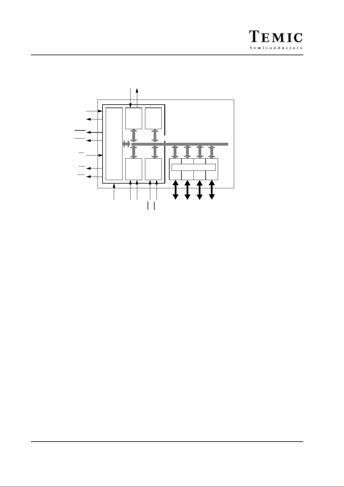
3. Block Diagram
RxD
(1)(1)
TxD
ALE/
XTAL1
XTAL2
PROG
PSEN
EA
RD
WR
(1)
(1)
CPU
RESET
EUART
Timer 0
Timer 1
(1) (1) (1) (1)
RAM
128x8
C51
CORE
INT
Ctrl
T0
T1
INT0
(1): Alternate function of Port 3
IB-bus
INT1
Parallel I/O Ports & Ext. Bus
Port 0
Port 1
P0
P1
Port 2
Port 3
P2
P3
2 Rev. A - Mar. 19, 1999
Preliminary
Page 3
TS80C31X2
4. SFR Mapping
The Special Function Registers (SFRs) of the TS80C31X2 fall into the following categories:
• C51 core registers: ACC, B, DPH, DPL, PSW, SP, AUXR1
• I/O port registers: P0, P1, P2, P3
• Timer registers: TCON, TH0, TH1, TMOD, TL0, TL1
• Serial I/O port registers: SADDR, SADEN, SBUF, SCON
• Power and clock control registers: PCON
• Interrupt system registers: IE, IP, IPH
• Others: CKCON
Table 1. All SFRs with their address and their reset value
Bit
address-
able
0/8 1/9 2/A 3/B 4/C 5/D 6/E 7/F
F8h FFh
F0h
E8h EFh
E0h
D8h DFh
D0h
C8h CFh
B
0000 0000
ACC
0000 0000
PSW
0000 0000
Non Bit addressable
F7h
E7h
D7h
C0h C7h
B8h
B0h
A8h
A0h
98h
90h
88h
80h
IP
XXX0 0000
P3
1111 1111
IE
0XX0 0000
P2
1111 1111
SCON
0000 0000
P1
1111 1111
TCON
0000 0000
P0
1111 1111
0/8 1/9 2/A 3/B 4/C 5/D 6/E 7/F
SADEN
0000 0000
SADDR
0000 0000
SBUF
XXXX XXXX
TMOD
0000 0000
SP
0000 0111
AUXR1
XXXX 0XX0
TL0
0000 0000
DPL
0000 0000
TL1
0000 0000
DPH
0000 0000
TH0
0000 0000
TH1
0000 0000
IPH
XXX0 0000
CKCON
XXXX XXX0
PCON
00X1 0000
BFh
B7h
AFh
A7h
9Fh
97h
8Fh
87h
reserved
Rev. A - Mar. 19, 1999 3
Preliminary
Page 4
TS80C31X2
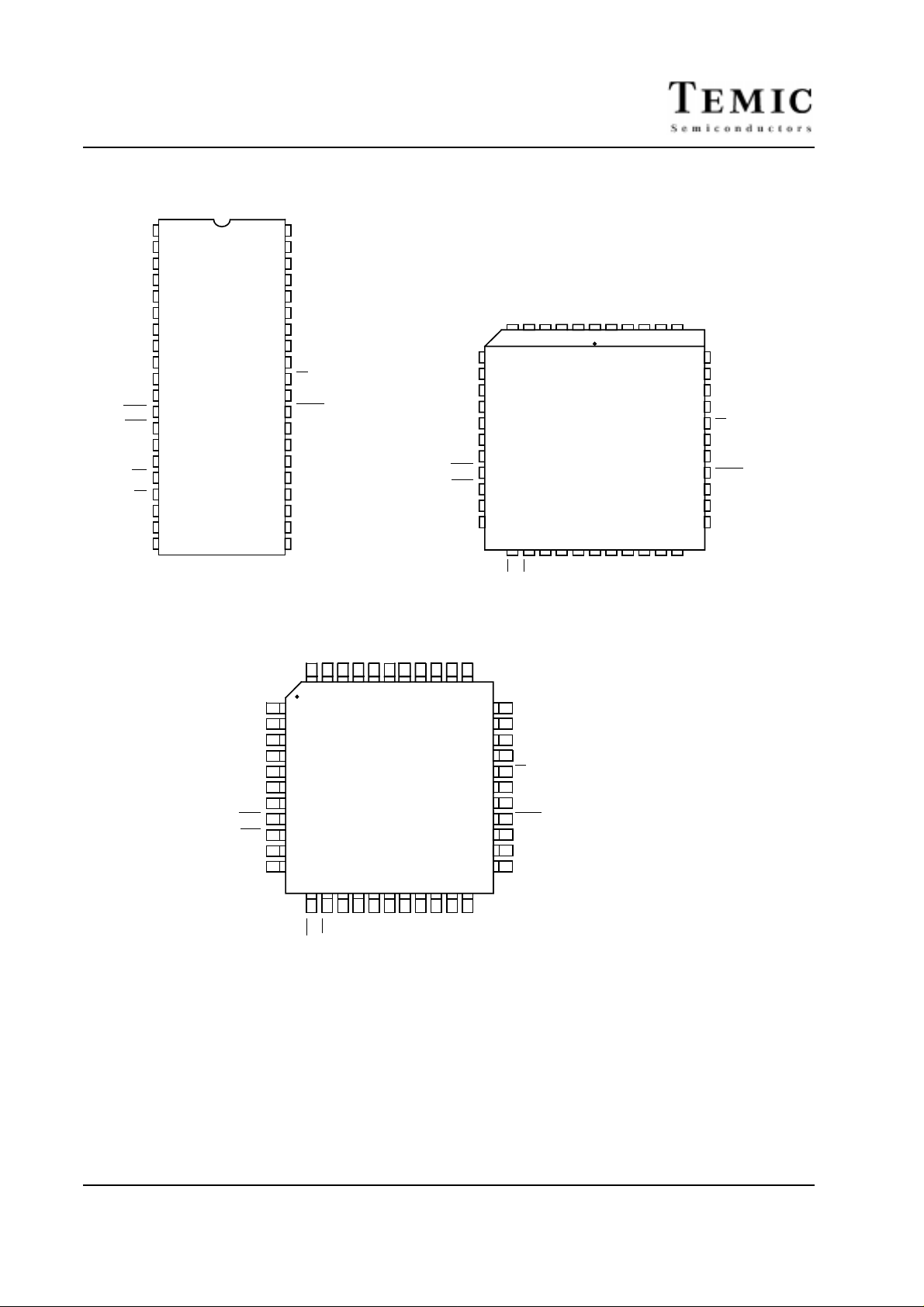
5. Pin Configuration
P1.0
P1.1
P1.2
P1.3
P1.4
P1.5
P1.6
P1.7
RST
P3.0/RxD
P3.1/TxD
P3.2/INT0
P3.3/INT1
P3.4/T0
P3.5/T1
P3.6/WR
P3.7/RD
XTAL2
XTAL1
VSS
1
3
4
5
9
10
11
14
15
16
17
2
6
7
8
12
13
18
19
20
PDIL40
24
40
31
30
26
VCC
39
P0.0
38
P0.1
P0.2
37
P0.3
36
P0.4
35
P0.5
34
P0.6
33
P0.7
32
EA
ALE
PSEN
29
P2.7
28
P2.6
27
P2.5
P2.4
25
P2.3
P2.2
23
P2.1
22
21
P2.0
P1.4
P1.3
P1.2
P1.1
P1.0
VSS1/NIC*
VCC
RST
P3.0/RxD
NIC*
P3.1/TxD
P3.2/INT0
P3.3/INT1
P3.4/T0
P3.5/T1
P0.0/AD0
P0.1/AD1
P1.5
P1.6
P1.7
P0.2/AD2
P1.4
7
8
9
10
11
12
13
14
15
16
17
P1.1
P1.3
P1.2
5 4 3 2 1 6
PLCC44
18 19 20 21 22 23 24 25 26 27 28
XTAL2
XTAL1
P3.7/RD
P3.6/WR
P0.3/AD3
P1.0
VSS1/NIC*
VCC
44 43 42 41 40
NIC*
VSS
P2.0/A8
P0.0/AD0
P2.1/A9
P0.2/AD2
P0.1/AD1
P2.2/A10
P2.3/A11
P0.3/AD3
39
38
37
36
35
34
33
32
31
30
29
P2.4/A12
P0.4/AD4
P0.5/AD5
P0.6/AD6
P0.7/AD7
EA
NIC*
ALE
PSEN
P2.7/A15
P2.6/A14
P2.5/A13
P3.2/INT0
*NIC: No Internal Connection
P1.5
P1.6
P1.7
RST
P3.0/RxD
NIC*
P3.1/TxD
P3.3/INT1
P3.4/T0
P3.5/T1
43 42 41 40 3944
1
2
3
4
5
6
7
8
9
10
11
38 37 36 35 34
PQFP44
VQFP44VQFP44
12 13 14 15 16 17 18 19 20 21 22
VSS
NIC*
XTAL1
P3.7/RD
P3.6/WR
XTAL2
P2.0/A8
P2.1/A9
P2.2/A10
33
32
31
30
29
28
27
26
25
24
23
P2.3/A11
P2.4/A12
P0.4/AD4
P0.5/AD5
P0.6/AD6
P0.7/AD7
EA
NIC*
ALE
PSEN
P2.7/A15
P2.6/A14
P2.5/A13
4 Rev. A - Mar. 19, 1999
Preliminary
Page 5
TS80C31X2
Table 2. Pin Description for 40/44 pin packages
MNEMONIC
V
SS
Vss1 1 39 I Optional Ground: Contact the Sales Office for ground connection.
V
CC
P0.0-P0.7 39-32 43-36 37-30 I/O Port 0: Port 0 is an open-drain, bidirectional I/O port. Port 0 pins that have 1s
P1.0-P1.7 1-8 2-9 40-44
P2.0-P2.7 21-28 24-31 18-25 I/O Port 2: Port 2 is an 8-bit bidirectional I/O port with internal pull-ups. Port 2
P3.0-P3.7 10-17 11,
Reset 9 10 4 I Reset: A high on this pin for two machine cycles while the oscillator is running,
ALE 30 33 27 O (I) Address Latch Enable: Output pulse for latching the low byte of the address
PSEN 29 32 26 O Program Store ENable: The read strobe to external program memory. When
EA 31 35 29 I
XTAL1 19 21 15 I
XTAL2 18 20 14 O Crystal 2: Output from the inverting oscillator amplifier
PIN NUMBER
DIL LCC VQFP 1.4
20 22 16 I Ground: 0V reference
40 44 38 I
1-3
5,
13-19
10 11 5 I RXD (P3.0): Serial input port
11 13 7 O TXD (P3.1): Serial output port
12 14 8 I INT0 (P3.2): External interrupt 0
13 15 9 I INT1 (P3.3): External interrupt 1
14 16 10 I T0 (P3.4): Timer 0 external input
15 17 11 I T1 (P3.5): Timer 1 external input
16 18 12 O WR (P3.6): External data memory write strobe
17 19 13 O RD (P3.7): External data memory read strobe
7-13
TYPE
Power Supply: This is the power supply voltage for normal, idle and power-
down operation
written to them float and can be used as high impedance inputs. Port 0 is also
the multiplexed low-orderaddress and data bus during access to external program
and data memory. In this application, it uses strong internal pull-up when emitting
1s.
I/O Port 1: Port 1 is an 8-bit bidirectional I/O port with internal pull-ups. Port 1
pins that have 1s written to them are pulled high by the internal pull-ups and
can be used as inputs. As inputs, Port 1 pins that are externally pulled low will
source current because of the internal pull-ups.
pins that have 1s written to them are pulled high by the internal pull-ups and
can be used as inputs. As inputs, Port 2 pins that are externally pulled low will
source current because of the internal pull-ups. Port 2 emits the high-order address
byte during fetches from external program memory and during accesses to external
data memory that use 16-bit addresses (MOVX @DPTR).In this application, it
uses strong internal pull-ups emitting 1s. During accesses to external data memory
that use 8-bit addresses (MOVX @Ri), port 2 emits the contents of the P2 SFR.
I/O Port 3: Port 3 is an 8-bit bidirectional I/O port with internal pull-ups. Port 3
pins that have 1s written to them are pulled high by the internal pull-ups and
can be used as inputs. As inputs, Port 3 pins that are externally pulled low will
source current because of the internal pull-ups. Port 3 also serves the special
features of the 80C51 family, as listed below.
resets the device. An internal diffused resistor to VSSpermits a power-on reset
using only an external capacitor to V
during an access to external memory. In normal operation, ALE is emitted at a
constant rate of 1/6 (1/3 in X2 mode) the oscillator frequency, and can be used
for external timing or clocking. Note that one ALE pulse is skipped during each
access to external data memory.
executing code from the external program memory, PSEN is activated twice each
machine cycle, except that two PSEN activations are skipped during each access
to external data memory. PSEN is not activated during fetches from internal
program memory.
External Access Enable: EA must be externally held low to enable the device
to fetch code from external program memory locations.
Crystal 1: Input to the inverting oscillator amplifier and input to the internal
clock generator circuits.
NAME AND FUNCTION
CC.
Rev. A - Mar. 19, 1999 5
Preliminary
Page 6
TS80C31X2
6. TS80C31X2 Enhanced Features
In comparison to the original 80C31, the TS80C31X2 implements some new features, which are:
• The X2 option.
• The Dual Data Pointer.
• The 4 level interrupt priority system.
• The power-off flag.
• The ONCE mode.
• Enhanced UART
6.1 X2 Feature
The TS80C31X2 core needs only 6 clock periods per machine cycle. This feature called ”X2” provides the following
advantages:
● Divide frequency crystals by 2 (cheaper crystals) while keeping same CPU power.
● Save power consumption while keeping same CPU power (oscillator power saving).
● Save power consumption by dividing dynamically operating frequency by 2 in operating and idle modes.
● Increase CPU power by 2 while keeping same crystal frequency.
In order to keep the original C51 compatibility, a divider by 2 is inserted between the XTAL1 signal and the main
clock input of the core (phase generator). This divider may be disabled by software.
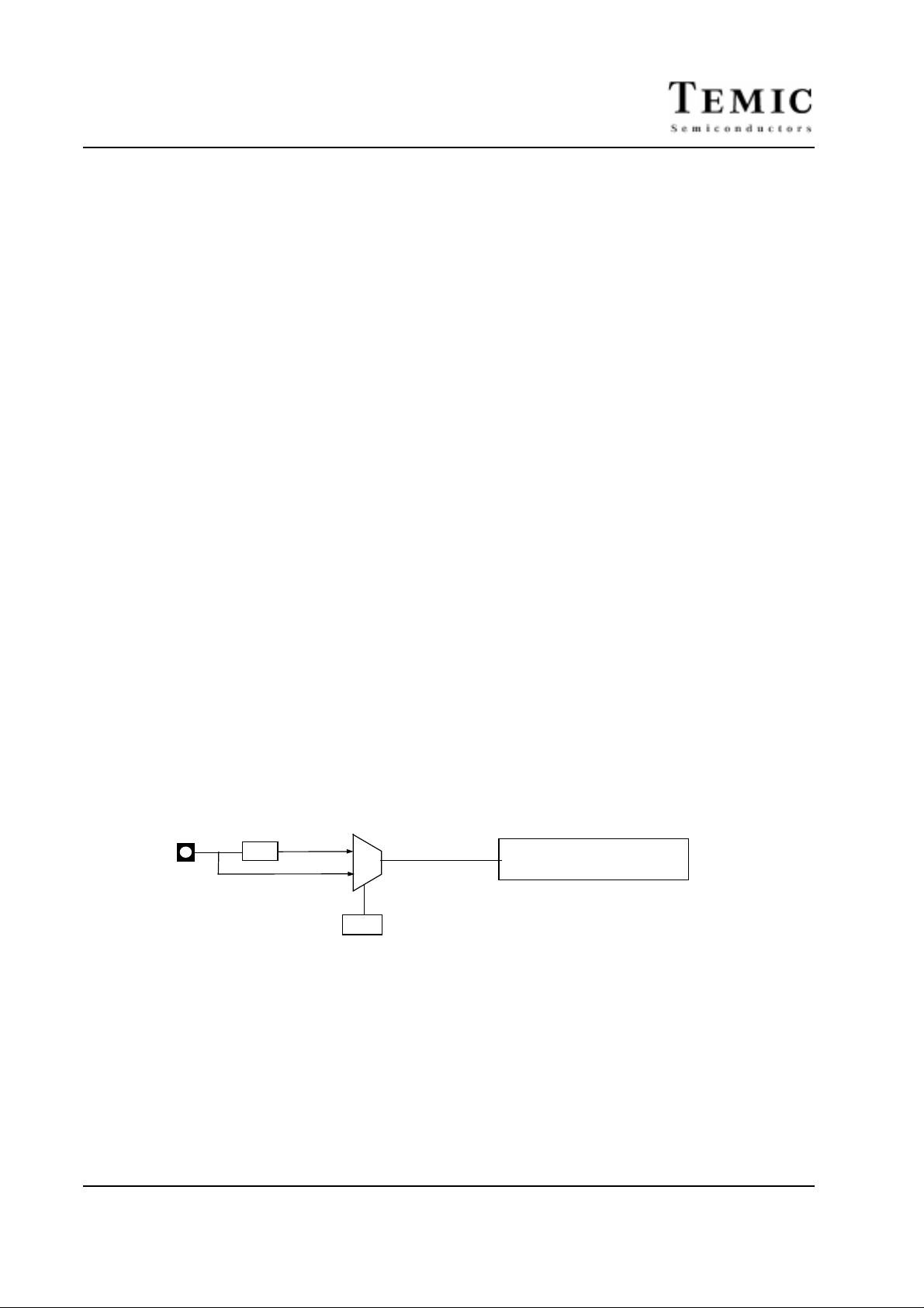
6.1.1 Description
The clock for the whole circuit and peripheral is first divided by two before being used by the CPU core and
peripherals. This allows any cyclic ratio to be accepted on XTAL1 input. In X2 mode, as this divider is bypassed,
the signals on XTAL1 must have a cyclic ratio between 40 to 60%. Figure 1. shows the clock generation block
diagram. X2 bit is validated on XTAL1÷2 rising edge to avoid glitches when switching from X2 to STD mode.
Figure 2. shows the mode switching waveforms.
XTAL1:2
XTAL1
F
XTAL
2
0
1
X2
CKCON reg
Figure 1. Clock Generation Diagram
F
OSC
state machine: 6 clock cycles.
CPU control
6 Rev. A - Mar. 19, 1999
Preliminary
Page 7
TS80C31X2
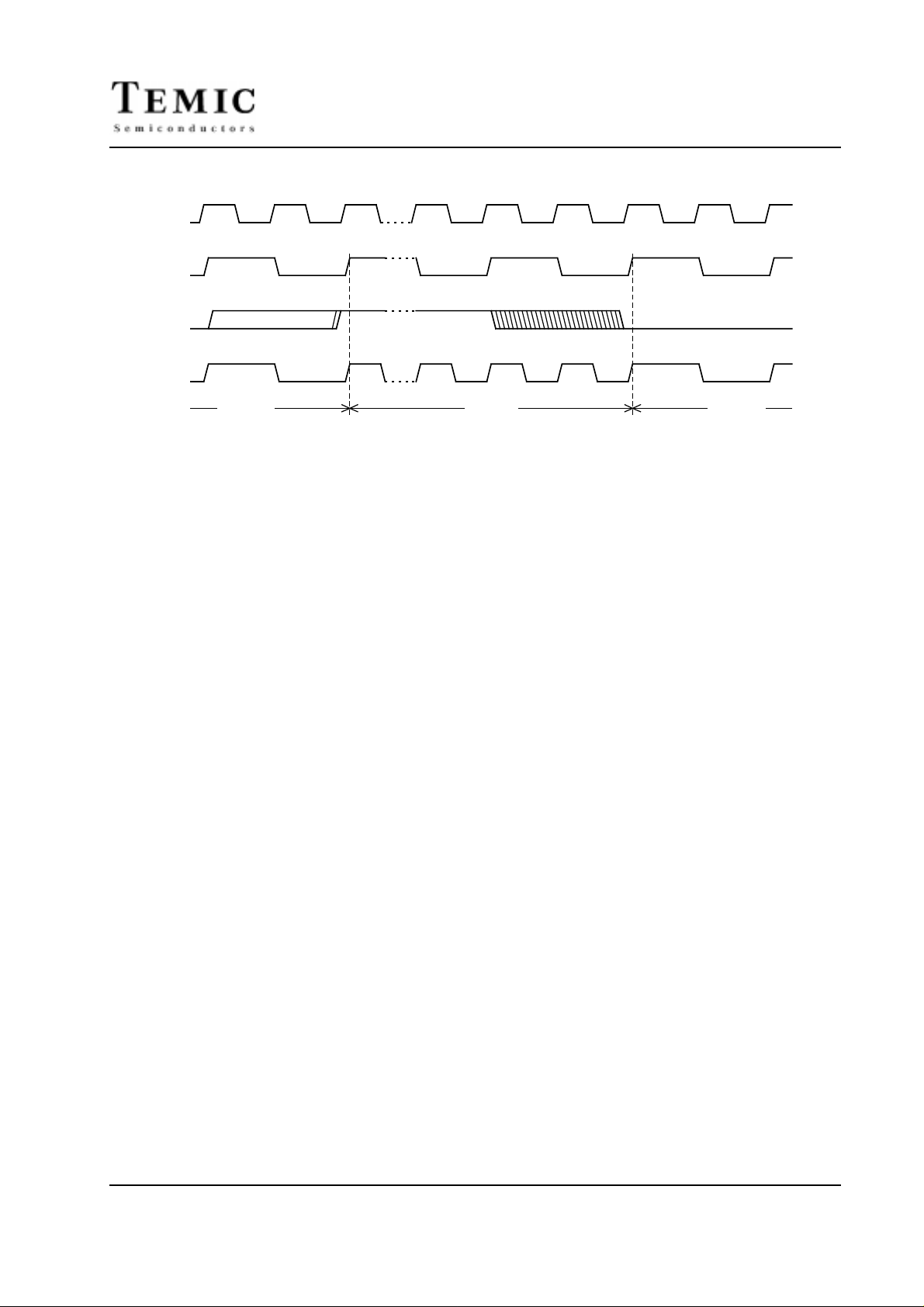
XTAL1
XTAL1:2
X2 bit
CPU clock
X2 ModeSTD Mode STD Mode
Figure 2. Mode Switching Waveforms
The X2 bit in the CKCON register (See Table 3.) allows to switch from 12 clock cycles per instruction to 6 clock
cycles and vice versa. At reset, the standard speed is activated (STD mode). Setting this bit activates the X2 feature
(X2 mode).
CAUTION
In order to prevent any incorrect operation while operating in X2 mode, user must be aware that all peripherals
using clock frequency as time reference (UART, timers) will have their time reference divided by two. For example
a free running timer generating an interrupt every 20 ms will then generate an interrupt every 10 ms. UART with
4800 baud rate will have 9600 baud rate.
Rev. A - Mar. 19, 1999 7
Preliminary
Page 8
TS80C31X2
Table 3. CKCON Register
CKCON - Clock Control Register (8Fh)
7 6 5 4 3 2 1 0
- - - - - - - X2
Bit
Number
7 -
6 -
5 -
4 -
3 -
2 -
1 -
0 X2
Bit
Mnemonic
Reserved
Reserved
Reserved
Reserved
Reserved
Reserved
Reserved
CPU and peripheral clock bit
Reset Value = XXXX XXX0b
Not bit addressable
Description
The value read from this bit is indeterminate. Do not set this bit.
The value read from this bit is indeterminate. Do not set this bit.
The value read from this bit is indeterminate. Do not set this bit.
The value read from this bit is indeterminate. Do not set this bit.
The value read from this bit is indeterminate. Do not set this bit.
The value read from this bit is indeterminate. Do not set this bit.
The value read from this bit is indeterminate. Do not set this bit.
Clear to select 12 clock periods per machine cycle (STD mode, F
Set to select 6 clock periods per machine cycle (X2 mode, F
OSC=FXTAL
OSC=FXTAL
).
/2).
8 Rev. A - Mar. 19, 1999
Preliminary
Page 9

TS80C31X2
6.2 Dual Data Pointer Register Ddptr
The additional data pointer can be used to speed up code execution and reduce code size in a number of
ways.
The dual DPTR structure is a way by which the chip will specify the address of an external data memory
location. There are two 16-bit DPTR registers that address the external memory, and a single bit called
DPS = AUXR1/bit0 (See Table 5.) that allows the program code to switch between them (Refer to Figure 3).
External Data Memory
07
DPS
AUXR1(A2H)
DPH(83H) DPL(82H)
DPTR1
DPTR0
Figure 3. Use of Dual Pointer
Rev. A - Mar. 19, 1999 9
Preliminary
Page 10
TS80C31X2
Table 4. AUXR1: Auxiliary Register 1
7 6 5 4 3 2 1 0
- - - - - - - DPS
Bit
Number
7 -
6 -
5 -
4 -
3 -
2 -
1 -
0 DPS
Bit
Mnemonic
Reserved
Reserved
Reserved
Reserved
Reserved
Reserved
Reserved
Data Pointer Selection
Reset Value = XXXX XXX0
Not bit addressable
Description
The value read from this bit is indeterminate. Do not set this bit.
The value read from this bit is indeterminate. Do not set this bit.
The value read from this bit is indeterminate. Do not set this bit.
The value read from this bit is indeterminate. Do not set this bit.
The value read from this bit is indeterminate. Do not set this bit.
The value read from this bit is indeterminate. Do not set this bit.
The value read from this bit is indeterminate. Do not set this bit.
Clear to select DPTR0.
Set to select DPTR1.
Application
Software can take advantage of the additional data pointers to both increase speed and reduce code size, for
example, block operations (copy, compare, search ...) are well served by using one data pointer as a ’source’
pointer and the other one as a "destination" pointer.
10 Rev. A - Mar. 19, 1999
Preliminary
Page 11

ASSEMBLY LANGUAGE
; Block move using dual data pointers
; Destroys DPTR0, DPTR1, A and PSW
; note: DPS exits opposite of entry state
; unless an extra INC AUXR1 is added
;
00A2 AUXR1 EQU 0A2H
;
0000 909000MOV DPTR,#SOURCE ; address of SOURCE
0003 05A2 INC AUXR1 ; switch data pointers
0005 90A000 MOV DPTR,#DEST ; address of DEST
0008 LOOP:
0008 05A2 INC AUXR1 ; switch data pointers
000A E0 MOVX A,@DPTR ; get a byte from SOURCE
000B A3 INC DPTR ; increment SOURCE address
000C 05A2 INC AUXR1 ; switch data pointers
000E F0 MOVX @DPTR,A ; write the byte to DEST
000F A3 INC DPTR ; increment DEST address
0010 70F6 JNZ LOOP ; check for 0 terminator
0012 05A2 INC AUXR1 ; (optional) restore DPS
TS80C31X2
INC is a short (2 bytes) and fast (12 clocks) way to manipulate the DPS bit in the AUXR1 SFR. However,
note that the INC instruction does not directly force the DPS bit to a particular state, but simply toggles it.
In simple routines, such as the block move example, only the fact that DPS is toggled in the proper sequence
matters, not its actual value. In other words, the block move routine works the same whether DPS is '0' or '1'
on entry. Observe that without the last instruction (INC AUXR1), the routine will exit with DPS in the
opposite state.
Rev. A - Mar. 19, 1999 11
Preliminary
Page 12
TS80C31X2
6.3 TS80C31X2 Serial I/O Port
The serial I/O port in the TS80C31X2 is compatible with the serial I/O port in the 80C31.
It provides both synchronous and asynchronous communication modes. It operates as an Universal Asynchronous
Receiver and Transmitter (UART) in three full-duplex modes (Modes 1, 2 and 3). Asynchronous transmission and
reception can occur simultaneously and at different baud rates
Serial I/O port includes the following enhancements:
● Framing error detection
● Automatic address recognition
6.3.1 Framing Error Detection
Framing bit error detection is provided for the three asynchronous modes (modes 1, 2 and 3). To enable the framing
bit error detection feature, set SMOD0 bit in PCON register (See Figure 4).
RITIRB8TB8RENSM2SM1SM0/FE
SCON (98h)
Set FE bit if stop bit is 0 (framing error) (SMOD = 1)
SM0 to UART mode control (SMOD = 0)
PCON (87h)
IDLPDGF0GF1POF-SMOD0SMOD1
To UART framing error control
Figure 4. Framing Error Block Diagram
When this feature is enabled, the receiver checks each incoming data frame for a valid stop bit. An invalid stop
bit may result from noise on the serial lines or from simultaneous transmission by two CPUs. If a valid stop bit
is not found, the Framing Error bit (FE) in SCON register (See Table 5.) bit is set.
12 Rev. A - Mar. 19, 1999
Preliminary
Page 13

TS80C31X2
Software may examine FE bit after each reception to check for data errors. Once set, only software or a reset can
clear FE bit. Subsequently received frames with valid stop bits cannot clear FE bit. When FE feature is enabled,
RI rises on stop bit instead of the last data bit (See Figure 5. and Figure 6.).
RXD
SMOD0=X
FE
SMOD0=1
SMOD0=0
SMOD0=1
SMOD0=1
D7D6D5D4D3D2D1D0
Start
bit
RI
Data byte
Stop
bit
Figure 5. UART Timings in Mode 1
RXD
RI
RI
FE
Start
bit
Data byte Ninth
D8D7D6D5D4D3D2D1D0
bit
Stop
bit
Figure 6. UART Timings in Modes 2 and 3
6.3.2 Automatic Address Recognition
The automatic address recognition feature is enabled when the multiprocessor communication feature is enabled
(SM2 bit in SCON register is set).
Implemented in hardware, automatic address recognition enhances the multiprocessor communication feature by
allowing the serial port to examine the address of each incoming command frame. Only when the serial port
recognizes its own address, the receiver sets RI bit in SCON register to generate an interrupt. This ensures that
the CPU is not interrupted by command frames addressed to other devices.
If desired, you may enable the automatic address recognition feature in mode 1. In this configuration, the stop bit
takes the place of the ninth data bit. Bit RI is set only when the received command frame address matches the
device’s address and is terminated by a valid stop bit.
To support automatic address recognition, a device is identified by a given address and a broadcast address.
NOTE: The multiprocessor communication and automatic address recognition features cannot be enabled in mode 0 (i.e. setting SM2 bit in SCON
register in mode 0 has no effect).
Rev. A - Mar. 19, 1999 13
Preliminary
Page 14

TS80C31X2
6.3.3 Given Address
Each device has an individual address that is specified in SADDR register; the SADEN register is a mask byte
that contains don’t-care bits (defined by zeros) to form the device’s given address. The don’t-care bits provide the
flexibility to address one or more slaves at a time. The following example illustrates how a given address is formed.
To address a device by its individual address, the SADEN mask byte must be 1111 1111b.
For example:
SADDR 0101 0110b
SADEN 1111 1100b
Given 0101 01XXb
The following is an example of how to use given addresses to address different slaves:
Slave A: SADDR 1111 0001b
SADEN 1111 1010b
Given 1111 0X0Xb
Slave B: SADDR 1111 0011b
Slave C: SADDR 1111 0010b
The SADEN byte is selected so that each slave may be addressed separately.
For slave A, bit 0 (the LSB) is a don’t-care bit; for slaves B and C, bit 0 is a 1. To communicate with slave A
only, the master must send an address where bit 0 is clear (e.g. 1111 0000b).
For slave A, bit 1 is a 1; for slaves B and C, bit 1 is a don’t care bit. To communicate with slaves B and C, but
not slave A, the master must send an address with bits 0 and 1 both set (e.g. 1111 0011b).
To communicate with slaves A, B and C, the master must send an address with bit 0 set, bit 1 clear, and bit 2
clear (e.g. 1111 0001b).
SADEN 1111 1001b
Given 1111 0XX1b
SADEN 1111 1101b
Given 1111 00X1b
6.3.4 Broadcast Address
A broadcast address is formed from the logical OR of the SADDR and SADEN registers with zeros defined as
don’t-care bits, e.g.:
SADDR 0101 0110b
Broadcast =SADDR OR SADEN 1111 111Xb
The use of don’t-care bits provides flexibility in defining the broadcast address, however in most applications, a
broadcast address is FFh. The following is an example of using broadcast addresses:
Slave A: SADDR 1111 0001b
SADEN 1111 1100b
SADEN 1111 1010b
Broadcast 1111 1X11b,
Slave B: SADDR 1111 0011b
Slave C: SADDR= 1111 0010b
For slaves A and B, bit 2 is a don’t care bit; for slave C, bit 2 is set. To communicate with all of the slaves, the
master must send an address FFh. To communicate with slaves A and B, but not slave C, the master can send
and address FBh.
14 Rev. A - Mar. 19, 1999
SADEN 1111 1001b
Broadcast 1111 1X11B,
SADEN 1111 1101b
Broadcast 1111 1111b
Preliminary
Page 15

TS80C31X2
6.3.5 Reset Addresses
On reset, the SADDR and SADEN registers are initialized to 00h, i.e. the given and broadcast addresses are XXXX
XXXXb (all don’t-care bits). This ensures that the serial port will reply to any address, and so, that it is backwards
compatible with the 80C51 microcontrollers that do not support automatic address recognition.
SADEN - Slave Address Mask Register (B9h)
7 6 5 4 3 2 1 0
Reset Value = 0000 0000b
Not bit addressable
SADDR - Slave Address Register (A9h)
7 6 5 4 3 2 1 0
Reset Value = 0000 0000b
Not bit addressable
Rev. A - Mar. 19, 1999 15
Preliminary
Page 16

TS80C31X2
Table 5. SCON Register
SCON - Serial Control Register (98h)
7 6 5 4 3 2 1 0
FE/SM0 SM1 SM2 REN TB8 RB8 TI RI
Bit
Number
7 FE
6 SM1
5 SM2
4 REN
3 TB8
Bit
Mnemonic
SM0
Description
Framing Error bit (SMOD0=1)
Clear to reset the error state, not cleared by a valid stop bit.
Set by hardware when an invalid stop bit is detected.
SMOD0 must be set to enable access to the FE bit
Serial port Mode bit 0
Refer to SM1 for serial port mode selection.
SMOD0 must be cleared to enable access to the SM0 bit
Serial port Mode bit 1
SM1 SM0 Mode Description Baud Rate
0 0 0 Shift Register F
0 1 1 8-bit UART Variable
1 0 2 9-bit UART F
1 1 3 9-bit UART Variable
Serial port Mode 2 bit / Multiprocessor Communication Enable bit
Clear to disable multiprocessor communication feature.
Set to enable multiprocessor communication feature in mode 2 and 3, and eventually mode 1. This bit should
be cleared in mode 0.
Reception Enable bit
Clear to disable serial reception.
Set to enable serial reception.
Transmitter Bit 8 / Ninth bit to transmit in modes 2 and 3.
Clear to transmit a logic 0 in the 9th bit.
Set to transmit a logic 1 in the 9th bit.
XTAL
XTAL
/12
/64 or F
XTAL
/32
2 RB8
1 TI
0 RI
Reset Value = 0000 0000b
Bit addressable
Receiver Bit 8 / Ninth bit received in modes 2 and 3
Cleared by hardware if 9th bit received is a logic 0.
Set by hardware if 9th bit received is a logic 1.
In mode 1, if SM2 = 0, RB8 is the received stop bit. In mode 0 RB8 is not used.
Transmit Interrupt flag
Clear to acknowledge interrupt.
Set by hardware at the end of the 8th bit time in mode 0 or at the beginning of the stop bit in the other
modes.
Receive Interrupt flag
Clear to acknowledge interrupt.
Set by hardware at the end of the 8th bit time in mode 0, see Figure 5. and Figure 6. in the other modes.
16 Rev. A - Mar. 19, 1999
Preliminary
Page 17

TS80C31X2
Table 6. PCON Register
PCON - Power Control Register (87h)
7 6 5 4 3 2 1 0
SMOD1 SMOD0 - POF GF1 GF0 PD IDL
Bit
Number
7 SMOD1
6 SMOD0
5 -
4 POF
3 GF1
2 GF0
1 PD
0 IDL
Bit
Mnemonic
Description
Serial port Mode bit 1
Set to select double baud rate in mode 1, 2 or 3.
Serial port Mode bit 0
Clear to select SM0 bit in SCON register.
Set to to select FE bit in SCON register.
Reserved
The value read from this bit is indeterminate. Do not set this bit.
Power-Off Flag
Clear to recognize next reset type.
Set by hardware when VCC rises from 0 to its nominal voltage. Can also be set by software.
General purpose Flag
Cleared by user for general purpose usage.
Set by user for general purpose usage.
General purpose Flag
Cleared by user for general purpose usage.
Set by user for general purpose usage.
Power-Down mode bit
Cleared by hardware when reset occurs.
Set to enter power-down mode.
Idle mode bit
Clear by hardware when interrupt or reset occurs.
Set to enter idle mode.
Reset Value = 00X1 0000b
Not bit addressable
Power-off flag reset value will be 1 only after a power on (cold reset). A warm reset doesn’t affect the value of this bit.
Rev. A - Mar. 19, 1999 17
Preliminary
Page 18

TS80C31X2
6.4 Interrupt System
The TS80C31X2 has a total of 5 interrupt vectors: two external interrupts (INT0 and INT1), two timer interrupts
(timers 0 and 1) and the serial port interrupt. These interrupts are shown in Figure 7.
INT0
TF0
INT1
TF1
IPH, IP
IE0
IE1
RI
TI
3
0
3
0
3
0
3
0
3
0
High priority
interrupt
Interrupt
polling
sequence, decreasing
from high to low priority
Low priority
Individual Enable
Global Disable
interrupt
Figure 7. Interrupt Control System
Each of the interrupt sources can be individually enabled or disabled by setting or clearing a bit in the Interrupt
Enable register (See Table 8.). This register also contains a global disable bit, which must be cleared to disable
all interrupts at once.
Each interrupt source can also be individually programmed to one out of four priority levels by setting or clearing
a bit in the Interrupt Priority register (See Table 9.) and in the Interrupt Priority High register (See Table 10.).
shows the bit values and priority levels associated with each combination.
18 Rev. A - Mar. 19, 1999
Preliminary
Page 19

TS80C31X2
Table 7. Priority Level Bit Values
IPH.x IP.x Interrupt Level Priority
0 0 0 (Lowest)
0 1 1
1 0 2
1 1 3 (Highest)
A low-priority interrupt can be interrupted by a high priority interrupt, but not by another low-priority interrupt.
A high-priority interrupt can’t be interrupted by any other interrupt source.
If two interrupt requests of different priority levels are received simultaneously, the request of higher priority level
is serviced. If interrupt requests of the same priority level are received simultaneously, an internal polling sequence
determines which request is serviced. Thus within each priority level there is a second priority structure determined
by the polling sequence.
Table 8. IE Register
IE - Interrupt Enable Register (A8h)
7 6 5 4 3 2 1 0
EA - - ES ET1 EX1 ET0 EX0
Bit
Number
7 EA
6 -
5 -
4 ES
3 ET1
2 EX1
1 ET0
0 EX0
Bit
Mnemonic
Description
Enable All interrupt bit
Clear to disable all interrupts.
Set to enable all interrupts.
If EA=1, each interrupt source is individually enabled or disabled by setting or clearing its own interrupt
enable bit.
Reserved
The value read from this bit is indeterminate. Do not set this bit.
Reserved
The value read from this bit is indeterminate. Do not set this bit.
Serial port Enable bit
Clear to disable serial port interrupt.
Set to enable serial port interrupt.
Timer 1 overflow interrupt Enable bit
Clear to disable timer 1 overflow interrupt.
Set to enable timer 1 overflow interrupt.
External interrupt 1 Enable bit
Clear to disable external interrupt 1.
Set to enable external interrupt 1.
Timer 0 overflow interrupt Enable bit
Clear to disable timer 0 overflow interrupt.
Set to enable timer 0 overflow interrupt.
External interrupt 0 Enable bit
Clear to disable external interrupt 0.
Set to enable external interrupt 0.
Reset Value = 0XX0 0000b
Bit addressable
Table 9. IP Register
Rev. A - Mar. 19, 1999 19
Preliminary
Page 20

TS80C31X2
IP - Interrupt Priority Register (B8h)
7 6 5 4 3 2 1 0
- - - PS PT1 PX1 PT0 PX0
Bit
Number
7 -
6 -
5 -
4 PS
3 PT1
2 PX1
1 PT0
0 PX0
Bit
Mnemonic
Reserved
Reserved
Reserved
Serial port Priority bit
Timer 1 overflow interrupt Priority bit
External interrupt 1 Priority bit
Timer 0 overflow interrupt Priority bit
External interrupt 0 Priority bit
Reset Value = XXX0 0000b
Bit addressable
Description
The value read from this bit is indeterminate. Do not set this bit.
The value read from this bit is indeterminate. Do not set this bit.
The value read from this bit is indeterminate. Do not set this bit.
Refer to PSH for priority level.
Refer to PT1H for priority level.
Refer to PX1H for priority level.
Refer to PT0H for priority level.
Refer to PX0H for priority level.
20 Rev. A - Mar. 19, 1999
Preliminary
Page 21
TS80C31X2
Table 10. IPH Register
IPH - Interrupt Priority High Register (B7h)
7 6 5 4 3 2 1 0
- - - PSH PT1H PX1H PT0H PX0H
Bit
Number
7 -
6 -
5 -
4 PSH
3 PT1H
2 PX1H
Bit
Mnemonic
Description
Reserved
The value read from this bit is indeterminate. Do not set this bit.
Reserved
The value read from this bit is indeterminate. Do not set this bit.
Reserved
The value read from this bit is indeterminate. Do not set this bit.
Serial port Priority High bit
PSH PS Priority Level
0 0 Lowest
01
10
1 1 Highest
Timer 1 overflow interrupt Priority High bit
PT1H PT1 Priority Level
0 0 Lowest
01
10
1 1 Highest
External interrupt 1 Priority High bit
PX1H PX1 Priority Level
0 0 Lowest
01
10
1 1 Highest
Timer 0 overflow interrupt Priority High bit
1 PT0H
External interrupt 0 Priority High bit
0 PX0H
Reset Value = XXX0 0000b
Not bit addressable
PT0H PT0 Priority Level
0 0 Lowest
01
10
1 1 Highest
PX0H PX0 Priority Level
0 0 Lowest
01
10
1 1 Highest
Rev. A - Mar. 19, 1999 21
Preliminary
Page 22

TS80C31X2
6.5 Idle mode
An instruction that sets PCON.0 causes that to be the last instruction executed before going into the Idle mode.
In the Idle mode, the internal clock signal is gated off to the CPU, but not to the interrupt, Timer, and Serial Port
functions. The CPU status is preserved in its entirely : the Stack Pointer, Program Counter, Program Status Word,
Accumulator and all other registers maintain their data during Idle. The port pins hold the logical states they had
at the time Idle was activated. ALE and PSEN hold at logic high levels.
There are two ways to terminate the Idle. Activation of any enabled interrupt will cause PCON.0 to be cleared by
hardware, terminating the Idle mode. The interrupt will be serviced, and following RETI the next instruction to
be executed will be the one following the instruction that put the device into idle.
The flag bits GF0 and GF1 can be used to give and indication if an interrupt occured during normal operation or
during an Idle. For example, an instruction that activates Idle can also set one or both flag bits. When Idle is
terminated by an interrupt, the interrupt service routine can examine the flag bits.
The over way of terminating the Idle mode is with a hardware reset. Since the clock oscillator is still running, the
hardware reset needs to be held active for only two machine cycles (24 oscillator periods) to complete the reset.
6.6 Power-Down Mode
To save maximum power, a power-down mode can be invoked by software (Refer to Table 6., PCON register).
In power-down mode, the oscillator is stopped and the instruction that invoked power-down mode is the last
instruction executed. The internal RAM and SFRs retain their value until the power-down mode is terminated.
VCCcan be lowered to save further power. Either a hardware reset or an external interrupt can cause an exit from
power-down. To properly terminate power-down, the reset or external interrupt should not be executed before V
is restored to its normal operating level and must be held active long enough for the oscillator to restart and stabilize.
CC
Only external interrupts INT0 and INT1 are useful to exit from power-down. For that, interrupt must be enabled
and configured as level or edge sensitive interrupt input.
Holding the pin low restarts the oscillator but bringing the pin high completes the exit as detailed in Figure 8.
When both interrupts are enabled, the oscillator restarts as soon as one of the two inputs is held low and power
down exit will be completed when the first input will be released. In this case the higher priority interrupt service
routine is executed.
Once the interrupt is serviced, the next instruction to be executed after RETI will be the one following the instruction
that put TS80C31X2 into power-down mode.
INT0
INT1
XTAL1
Power-down phase Oscillator restart phase Active phaseActive phase
Figure 8. Power-Down Exit Waveform
Exit from power-down by reset redefines all the SFRs, exit from power-down by external interrupt does no affect
the SFRs.
Exit from power-down by either reset or external interrupt does not affect the internal RAM content.
NOTE:If idle mode is activated with power-downmode (IDL and PD bitsset),the exitsequenceisunchanged,when execution is vectored to interrupt,
PD and IDL bits are cleared and idle mode is not entered.
22 Rev. A - Mar. 19, 1999
Preliminary
Page 23

TS80C31X2
Table 11. The state of ports during idle and power-down modes
Mode
Idle External 1 1 Floating Port Data Address Port Data
Power Down External 0 0 Floating Port Data Port Data Port Data
Program
Memory
ALE PSEN PORT0 PORT1 PORT2 PORT3
Rev. A - Mar. 19, 1999 23
Preliminary
Page 24

TS80C31X2
6.7 ONCE Mode (ON Chip Emulation)
The ONCE mode facilitates testing and debugging of systems using TS80C31X2 without removing the circuit from
the board. The ONCE mode is invoked by driving certain pins of the TS80C31X2; the following sequence must
be exercised:
● Pull ALE low while the device is in reset (RST high) and PSEN is high.
● Hold ALE low as RST is deactivated.
While the TS80C31X2 is in ONCE mode, an emulator or test CPU can be used to drive the circuit Table 26.
shows the status of the port pins during ONCE mode.
Normal operation is restored when normal reset is applied.
Table 12. External Pin Status during ONCE Mode
ALE PSEN Port 0 Port 1 Port 2 Port 3 XTAL1/2
Weak pull-up Weak pull-up Float Weak pull-up Weak pull-up Weak pull-up Active
24 Rev. A - Mar. 19, 1999
Preliminary
Page 25
TS80C31X2
6.8 Power-Off Flag
The power-off flag allows the user to distinguish between a “cold start” reset and a “warm start” reset.
A cold start reset is the one induced by VCCswitch-on. A warm start reset occurs while VCCis still applied to
the device and could be generated for example by an exit from power-down.
The power-off flag (POF) is located in PCON register (See Table 13.). POF is set by hardware when VCCrises
from 0 to its nominal voltage. The POF can be set or cleared by software allowing the user to determine the type
of reset.
Table 13. PCON Register
PCON - Power Control Register (87h)
7 6 5 4 3 2 1 0
SMOD1 SMOD0 - POF GF1 GF0 PD IDL
Bit
Number
7 SMOD1
6 SMOD0
5 -
4 POF
3 GF1
2 GF0
1 PD
0 IDL
Bit
Mnemonic
Description
Serial port Mode bit 1
Set to select double baud rate in mode 1, 2 or 3.
Serial port Mode bit 0
Clear to select SM0 bit in SCON register.
Set to to select FE bit in SCON register.
Reserved
The value read from this bit is indeterminate. Do not set this bit.
Power-Off Flag
Clear to recognize next reset type.
Set by hardware when VCC rises from 0 to its nominal voltage. Can also be set by software.
General purpose Flag
Cleared by user for general purpose usage.
Set by user for general purpose usage.
General purpose Flag
Cleared by user for general purpose usage.
Set by user for general purpose usage.
Power-Down mode bit
Cleared by hardware when reset occurs.
Set to enter power-down mode.
Idle mode bit
Clear by hardware when interrupt or reset occurs.
Set to enter idle mode.
Reset Value = 00X1 0000b
Not bit addressable
Rev. A - Mar. 19, 1999 25
Preliminary
Page 26

TS80C31X2
7. Electrical Characteristics
7.1 Absolute Maximum Ratings
Ambiant Temperature Under Bias:
C = commercial 0°Cto70°C
I = industrial -40°Cto85°C
Storage Temperature -65°Cto+150°C
Voltage on VCCto V
Voltage on Any Pin to V
Power Dissipation 1 W
NOTES
1.
Stresses at or above those listed under “ Absolute Maximum Ratings” may cause permanent damage to the device. This is a stress rating only
and functional operation of the device at these or any other conditions above those indicated in the operational sections of this specification is not
implied. Exposure to absolute maximum rating conditions may affect device reliability.
2. This value is based on the maximum allowable die temperature and the thermal resistance of the package.
SS
SS
(1)
-0.5Vto+7V
-0.5VtoVCC+ 0.5 V
(2)
26 Rev. A - Mar. 19, 1999
Preliminary
Page 27

TS80C31X2
7.2 DC Parameters for Standard Voltage
TA =0°Cto+70°C; VSS=0V;VCC=5V± 10%;F=0to40MHz.
TA = -40°Cto+85°C; VSS=0V;VCC=5V± 10%;F=0to40MHz.
Table 14. DC Parameters in Standard Voltage
Symbol Parameter Min Typ Max Unit Test Conditions
V
V
V
V
V
V
Input Low Voltage -0.5 0.2 VCC - 0.1 V
IL
Input High Voltage except XTAL1, RST 0.2 VCC+ 0.9 VCC + 0.5 V
IH
Input High Voltage, XTAL1, RST 0.7 V
IH1
OL
Output Low Voltage, ports 1, 2, 3
OL1
Output Low Voltage, port 0, ALE, PSEN
Output High Voltage, ports 1, 2, 3 VCC - 0.3
OH
(6)
(6)
CC
VCC - 0.7
- 1.5
V
CC
VCC + 0.5 V
0.3
0.45
1.0
0.3
0.45
1.0
V
V
V
V
V
V
V
V
V
IOL = 100 µA
IOL = 1.6 mA
IOL = 3.5 mA
IOL = 200 µA
IOL = 3.2 mA
IOL = 7.0 mA
IOH = -10 µA
IOH = -30 µA
IOH = -60 µA
(4)
(4)
(4)
(4)
(4)
(4)
VCC = 5 V ± 10%
V
Output High Voltage, port 0, ALE, PSEN VCC - 0.3
OH1
VCC - 0.7
VCC - 1.5
V
V
V
IOH = -200 µA
IOH = -3.2 mA
IOH = -7.0 mA
VCC = 5 V ± 10%
R
RST Pulldown Resistor 50
RST
(5)
90
200 kΩ
I
Logical 0 Input Current ports 1, 2 and 3 -50 µA Vin = 0.45 V
IL
I
Input Leakage Current ±10 µA 0.45 V < Vin < V
LI
I
C
I
I
Logical 1 to 0 Transition Current, ports 1, 2, 3 -650 µA Vin = 2.0 V
TL
Capacitance of I/O Buffer 10 pF Fc = 1 MHz
IO
Power Down Current
PD
CC
Power Supply Current
Freq = 1 MHz
(7)
Icc op
Icc idle
(5)
10
50 µA
1.8
1
mA
mA
T
A = 25°C
2.0 V < V
VCC = 5.5 V
CC <
5.5 V
(1)
CC
(3)
Freq = 6 MHz
Icc op
Icc idle
(5)
10
4
mA
mA
VCC = 5.5 V
(2)
Freq ≥ 12 MHz
Icc op = 1.25 Freq (MHz) + 5 mA
Icc idle = 0.36 Freq (MHz) + 2.7 mA
13@12 MHz
16@16MHz
5.5@12Mz
7@16 MHz
mA
mA
Rev. A - Mar. 19, 1999 27
Preliminary
Page 28

TS80C31X2
7.3 DC Parameters for Low Voltage
TA =0°Cto+70°C; VSS=0V;VCC= 2.7 V to 5.5 V ± 10%;F=0to30MHz.
TA = -40°Cto+85°C; VSS=0V;VCC= 2.7 V to 5.5 V ± 10%;F=0to30MHz.
Table 15. DC Parameters for Low Voltage
Symbol Parameter Min Typ Max Unit Test Conditions
V
V
V
V
V
OL1
V
V
OH1
I
I
I
R
RST
Input Low Voltage -0.5 0.2 VCC - 0.1 V
IL
Input High Voltage except XTAL1, RST 0.2 VCC + 0.9 VCC + 0.5 V
IH
Input High Voltage, XTAL1, RST 0.7 V
IH1
OL
Output Low Voltage, ports 1, 2, 3
Output Low Voltage, port 0, ALE, PSEN
Output High Voltage, ports 1, 2, 3 0.9 V
OH
(6)
(6)
Output High Voltage, port 0, ALE, PSEN 0.9 V
Logical 0 Input Current ports 1, 2 and 3 -50 µA Vin = 0.45 V
IL
Input Leakage Current ±10 µA 0.45 V < Vin < V
LI
Logical 1 to 0 Transition Current, ports 1, 2, 3 -650 µA Vin = 2.0 V
TL
RST Pulldown Resistor 50
CC
CC
CC
(5)
90
VCC + 0.5 V
0.45 V
0.45 V
V IOH = -10 µA
V IOH = -40 µA
200 kΩ
IOL = 0.8 mA
IOL = 1.6 mA
CIO Capacitance of I/O Buffer 10 pF Fc = 1 MHz
A = 25°C
T
I
I
Power Down Current
PD
CC
Power Supply Current
(7)
Active Mode 16MHz
Idle Mode 16MHz
TBD
TBD
TBD
(5)
(5)
(5)
TBD µA
TBD
TBD
mA
mA
VCC = 2.0 V to 5.5 V
VCC = 3.3 V
VCC = 3.3 V
(4)
(4)
CC
(3)
(1)
(2)
NOTES
1. Operating ICC is measured with all output pins disconnected; XTAL1 driven with T
CLCH
, T
= 5 ns (see Figure 12.), VIL = VSS + 0.5 V,
CHCL
VIH = VCC - 0.5V; XTAL2 N.C.; EA = RST = Port 0 = VCC. ICC would be slightly higher if a crystal oscillator used..
2. Idle ICCis measured with all output pins disconnected; XTAL1 driven with T
CLCH,TCHCL
= 5 ns, VIL=VSS+ 0.5 V, VIH=VCC- 0.5 V;XTAL2
N.C; Port 0 = VCC; EA = RST = VSS (see Figure 10.).
3. Power Down ICC is measured with all output pins disconnected; EA = VSS, PORT 0 = VCC; XTAL2 NC.; RST = VSS (see Figure 11.).
4. Capacitance loading on Ports0 and 2 may cause spurious noise pulses to be superimposed on the VOLs of ALE and Ports1 and 3. The noise is
due to external bus capacitance discharginginto the Port 0 and Port 2 pins when these pins make 1 to 0 transitions during bus operation. In the worst
cases (capacitive loading 100pF), the noise pulse on the ALE line may exceed 0.45V with maxi V
peak 0.6V. A Schmitt Triggeruse is not necessary.
OL
5. Typicals are based on a limited number of samples and are not guaranteed. The values listed are at room temperature and 5V.
6. Under steady state (non-transient) conditions, IOL must be externally limited as follows:
Maximum IOL per port pin: 10 mA
Maximum IOL per 8-bit port:
Port 0: 26 mA
Ports 1, 2 and 3: 15 mA
Maximum total I
for all output pins: 71 mA
OL
IfIOLexceedsthe test condition,VOLmayexceed the relatedspecification. Pins arenot guaranteed to sinkcurrentgreaterthan the listed test conditions.
7. For other values, please contact your sales office.
28 Rev. A - Mar. 19, 1999
Preliminary
Page 29

TS80C31X2
V
CC
I
CC
V
CC
V
CC
V
CC
RST
P0
EA
(NC)
CLOCK
SIGNAL
XTAL2
XTAL1
V
SS
Figure 9. ICCTest Condition, Active Mode
V
CC
I
CC
V
CC
V
CC
P0
RST
EA
(NC)
CLOCK
SIGNAL
XTAL2
XTAL1
V
SS
Figure 10. ICCTest Condition, Idle Mode
All other pins are disconnected.
All other pins are disconnected.
V
CC
I
CC
V
CC
V
CC
P0
RST
EA
(NC)
XTAL2
XTAL1
V
SS
All other pins are disconnected.
Figure 11. ICCTest Condition, Power-Down Mode
Rev. A - Mar. 19, 1999 29
Preliminary
Page 30

TS80C31X2
VCC-0.5V
0.45V
T
CHCL
T
CLCH
= T
CHCL
= 5ns.
T
CLCH
0.7V
CC
0.2VCC-0.1
Figure 12. Clock Signal Waveform for ICCTests in Active and Idle Modes
7.4 AC Parameters
7.4.1 Explanation of the AC Symbols
Each timing symbol has 5 characters. The first character is always a “T” (stands for time). The other characters,
depending on their positions, stand for the name of a signal or the logical status of that signal. The following is
a list of all the characters and what they stand for.
Example:T
T
= Time for ALE Low to PSEN Low.
LLPL
TA =0to+70°C; VSS=0V;VCC=5V± 10%; -M and -V ranges.
TA = -40°Cto+85°C; VSS=0V; VCC=5V± 10%; -M and -V ranges.
TA =0to+70°C; VSS=0V;2.7V<V
TA = -40°Cto+85°C; VSS=0V;2.7V<V
(Load Capacitance for port 0, ALE and PSEN = 100 pF; Load Capacitance for all other outputs = 80 pF.)
Table 16., Table 19. and Table 22. give the description of each AC symbols.
= Time for Address Valid to ALE Low.
AVLL
CC <
5.5 V; -L range.
5.5 V; -L range.
CC <
Table 17., Table 20. and Table 23. give for each range the AC parameter.
Table 18., Table 21. and Table 24. give the frequency derating formula of the AC parameter. To calculate each
AC symbols, take the x value corresponding to the speed grade you need (-M, -V or -L) and replace this value
in the formula.
Example:
T
in X2 mode for a -V part at 25 MHz:
LLIV
x= 22
T= 40ns
T
=2T-x=2x40-22=58ns
LLIV
30 Rev. A - Mar. 19, 1999
Preliminary
Page 31

7.4.2 External Program Memory Characteristics
Table 16. Symbol Description
Symbol Parameter
T Oscillator clock period
TS80C31X2
T
T
T
T
T
T
T
T
T
T
T
T
LHLL
AVLL
LLAX
LLIV
LLPL
PLPH
PLIV
PXIX
PXIZ
PXAV
AVIV
PLAZ
ALE pulse width
Address Valid to ALE
Address Hold After ALE
ALE to Valid Instruction In
ALE to PSEN
PSEN Pulse Width
PSEN to Valid Instruction In
Input Instruction Hold After PSEN
Input Instruction FloatAfter PSEN
PSEN to Address Valid
Address to Valid Instruction In
PSEN Low to Address Float
Table 17. AC Parameters for Fix Clock
Speed
(see ordering)
Symbol Min Max Min Max Min Max
-M -V -L Units
T 25 17 50 ns
T
T
T
T
T
T
T
T
T
T
T
T
LHLL
AVLL
LLAX
LLIV
LLPL
PLPH
PLIV
PXIX
PXIZ
PXAV
AVIV
PLAZ
40 25 60 ns
10 7 20 ns
10 7 20 ns
70 45 125 ns
10 7 20 ns
60 45 105 ns
25 25 60 ns
0 0 0 ns
18 12 30 ns
18 12 30 ns
85 53 145 ns
10 10 10 ns
Rev. A - Mar. 19, 1999 31
Preliminary
Page 32

TS80C31X2
Table 18. AC Parameters for a Variable Clock
Symbol Type Standard
X2 Clock -M -V -L Units
Clock
T
T
AVLL
T
LLAX
T
T
T
T
T
T
T
PXAV
T
T
LHLL
LLIV
LLPL
PLPH
PLIV
PXIX
PXIZ
AVIV
PLAZ
Min 2 T - x T - x 10 8 40 ns
Min T - x 0.5 T - x 15 10 30 ns
Min T - x 0.5 T - x 15 10 30 ns
Max 4 T - x 2 T - x 30 22 75 ns
Min T - x 0.5 T - x 15 10 30 ns
Min 3 T - x 1.5 T - x 15 5 45 ns
Max 3 T - x 1.5 T - x 50 25 90 ns
Min x x 0 0 0 ns
Max T - x 0.5 T - x 7 5 20 ns
Min T - x 0.5 T - x 7 5 20 ns
Max 5 T - x 2.5 T - x 40 30 105 ns
Max x x 10 10 10 ns
7.4.3 External Program Memory Read Cycle
ALE
PSEN
PORT 0
PORT 2
ADDRESS
OR SFR-P2
12 T
CLCL
T
LHLL
T
T
LLAX
AVLL
T
LLIV
T
LLPL
T
PLIV
TPLAZ
T
PLPH
T
PXIX
T
PXIZ
T
PXAV
A0-A7A0-A7 INSTR ININSTR IN INSTR IN
T
AVIV
Figure 13. External Program Memory Read Cycle
ADDRESS A8-A15ADDRESS A8-A15
32 Rev. A - Mar. 19, 1999
Preliminary
Page 33

7.4.4 External Data Memory Characteristics
Table 19. Symbol Description
Symbol Parameter
TS80C31X2
T
T
WLWH
T
T
RHDX
T
T
T
AVDV
T
T
AVWL
T
QVWX
T
QVWH
T
WHQX
T
T
WHLH
RLRH
RLDV
RHDZ
LLDV
LLWL
RLAZ
RD Pulse Width
WR Pulse Width
RD to Valid Data In
Data Hold After RD
Data Float After RD
ALE to Valid Data In
Address to Valid Data In
ALE to WR or RD
Address to WR or RD
Data Valid to WR Transition
Data set-up to WR High
Data Hold After WR
RD Low to Address Float
RD or WR High to ALE high
Rev. A - Mar. 19, 1999 33
Preliminary
Page 34

TS80C31X2
Table 20. AC Parameters for a Fix Clock
Speed
-M -V -L Units
(see ordering)
Symbol Min Max Min Max Min Max
T
RLRH
T
WLWH
T
RLDV
T
RHDX
T
RHDZ
T
LLDV
T
AVDV
T
LLWL
T
AVWL
T
QVWX
T
QVWH
T
WHQX
105 85 200 ns
105 90 200 ns
100 60 155 ns
0 0 0 ns
15 13 40 ns
160 100 310 ns
165 100 360 ns
40 110 30 65 90 60 ns
40 27 100 ns
3 0 18 ns
145 90 280 ns
10 7 20 ns
T
RLAZ
T
WHLH
0 0 0 ns
5 45 5 29 20 80 ns
34 Rev. A - Mar. 19, 1999
Preliminary
Page 35

Table 21. AC Parameters for a Variable Clock
TS80C31X2
Symbol Type Standard
Clock
T
T
WLWH
T
T
RHDX
T
T
T
AVDV
T
T
T
AVWL
T
QVWX
T
QVWH
T
WHQX
RLRH
RLDV
RHDZ
LLDV
LLWL
LLWL
Min 6 T - x 3 T - x 45 15 100 ns
Min 6 T - x 3 T - x 45 10 100 ns
Max 5 T - x 2.5 T - x 25 23 95 ns
Min x x 0 0 0 ns
Max 2 T - x T - x 35 20 60 ns
Max 8 T - x 4T -x 40 33 90 ns
Max 9 T - x 4.5 T - x 60 50 90 ns
Min 3 T - x 1.5 T - x 35 20 60 ns
Max 3 T + x 1.5 T + x 35 15 60 ns
Min 4 T - x 2 T - x 60 40 100 ns
Min T - x 0.5 T - x 22 17 32 ns
Min 7 T - x 3.5 T - x 30 27 70 ns
Min T - x 0.5 T - x 15 10 30 ns
X2 Clock -M -V -L Units
T
RLAZ
T
WHLH
T
WHLH
Max x x 0 0 0 ns
Min T - x 0.5 T - x 20 12 30 ns
Max T + x 0.5 T + x 20 12 30 ns
7.4.5 External Data Memory Write Cycle
ALE
PSEN
WR
PORT 0
PORT 2
ADDRESS
OR SFR-P2
Figure 14. External Data Memory Write Cycle
T
LLAX
T
LLWL
T
QVWX
T
QVWH
T
WLWH
A0-A7 DATA OUT
T
AVWL
ADDRESS A8-A15 OR SFR P2
T
WHLH
T
WHQX
Rev. A - Mar. 19, 1999 35
Preliminary
Page 36
TS80C31X2
7.4.6 External Data Memory Read Cycle
ALE
T
LLDV
T
WHLH
PSEN
RD
T
LLAX
PORT 0
PORT 2
ADDRESS
OR SFR-P2
A0-A7 DATA IN
T
AVWL
Figure 15. External Data Memory Read Cycle
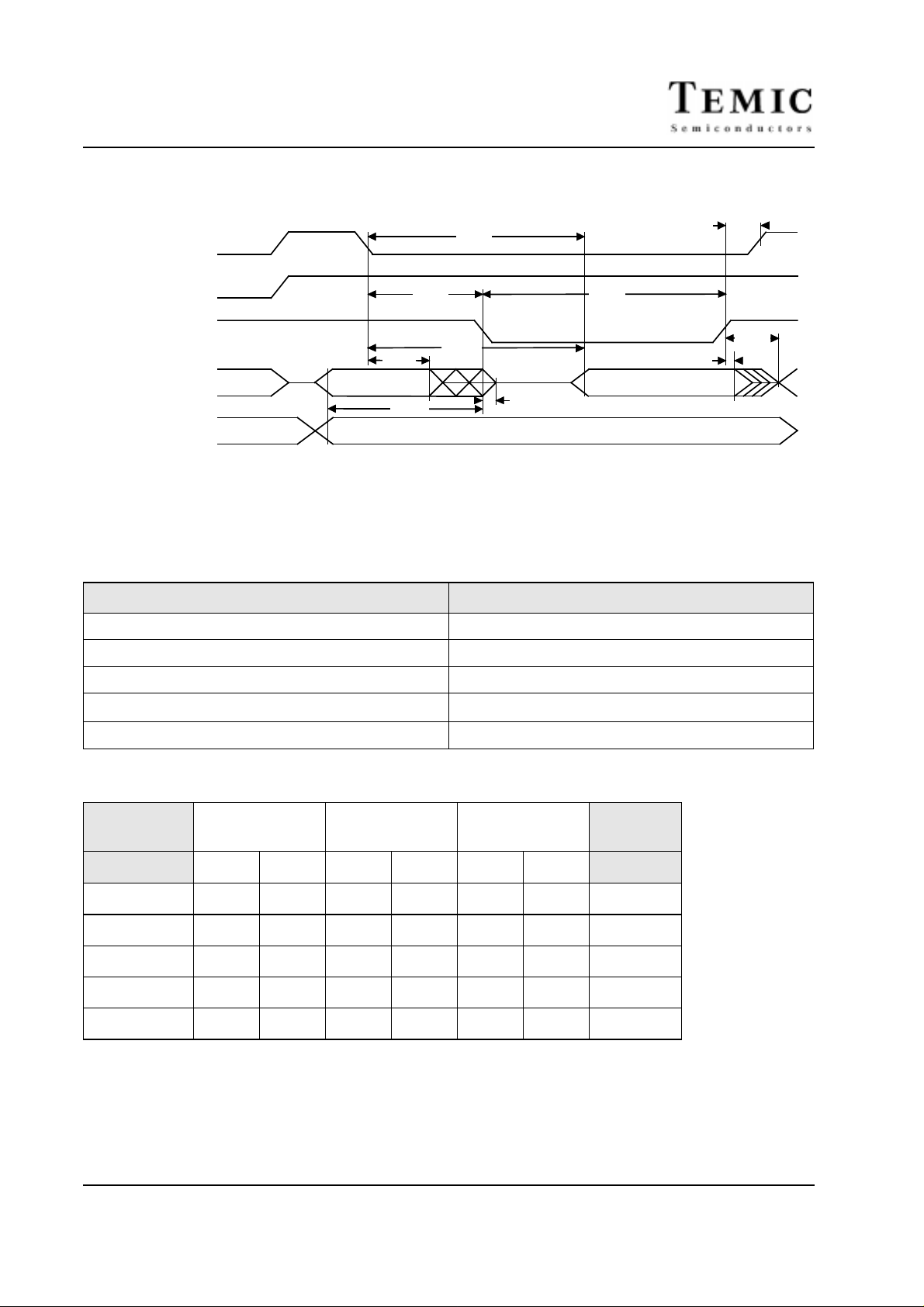
7.4.7 Serial Port Timing - Shift Register Mode
Table 22. Symbol Description
Symbol Parameter
T
XLXL
T
QVHX
T
XHQX
T
XHDX
T
XHDV
T
LLWL
T
AVDV
T
RLAZ
ADDRESS A8-A15 OR SFR P2
Serial port clock cycle time
Output data set-up to clock rising edge
Output data hold after clock rising edge
Input data hold after clock rising edge
Clock rising edge to input data valid
T
RLRH
T
RHDX
T
RHDZ
Table 23. AC Parameters for a Fix Clock
Speed
(see ordering)
Symbol Min Max Min Max Min Max
T
XLXL
T
QVHX
T
XHQX
T
XHDX
T
XHDV
-M -V -L
300 200 600 ns
200 117 367 ns
20 13 50 ns
0 0 0 ns
200 117 367 ns
Units
36 Rev. A - Mar. 19, 1999
Preliminary
Page 37

Table 24. AC Parameters for a Variable Clock
TS80C31X2
Symbol Type Standard
X2 Clock -M -V -L
Clock
T
XLXL
T
QVHX
T
XHQX
T
XHDX
T
XHDV
Min 12 T 6 T ns
Min 10 T - x 5 T - x 50 50 133 ns
Min 2 T - x T - x 30 20 50 ns
Min x x 0 0 0 ns
Max 10 T - x 5 T- x 50 50 133 ns
7.4.8 Shift Register Timing Waveforms
INSTRUCTION
ALE
CLOCK
OUTPUT DATA
WRITE to SBUF
INPUT DATA
0123456 87
T
XLXL
T
QVXH
01234567
T
XHDV
VALID VALIDVALID
T
XHQX
VALID
T
XHDX
Units
SET TI
VALID VALID VALID VALID
CLEAR RI
SET RI
Figure 16. Shift Register Timing Waveforms
Rev. A - Mar. 19, 1999 37
Preliminary
Page 38

TS80C31X2
7.4.9 External Clock Drive Characteristics (XTAL1)
Table 25. AC Parameters
Symbol Parameter Min Max Units
T
CLCL
T
CHCX
T
CLCX
T
CLCH
T
CHCL
T
CHCX/TCLCX
Oscillator Period 25 ns
High Time 5 ns
Low Time 5 ns
Rise Time 5 ns
Fall Time 5 ns
Cyclic ratio in X2 mode 40 60 %
7.4.10 External Clock Drive Waveforms
VCC-0.5 V
0.45 V
0.7V
CC
0.2VCC-0.1 V
T
CHCL
Figure 17. External Clock Drive Waveforms
T
CLCX
T
CLCL
T
CLCH
T
CHCX
7.4.11 AC Testing Input/Output Waveforms
VCC-0.5 V
INPUT/OUTPUT
0.45 V
Figure 18. AC Testing Input/Output Waveforms
AC inputs during testing are driven at VCC- 0.5 for a logic “1” and 0.45V for a logic “0”. Timing measurement
are made at VIHmin for a logic “1” and VILmax for a logic “0”.
0.2VCC+0.9
0.2VCC-0.1
7.4.12 Float Waveforms
FLOAT
VOH-0.1 V
VOL+0.1 V
V
LOAD
V
V
LOAD
LOAD
Figure 19. Float Waveforms
+0.1 V
-0.1 V
38 Rev. A - Mar. 19, 1999
Preliminary
Page 39

TS80C31X2
For timing purposes as port pin is no longer floating when a 100 mV change from load voltage occurs and begins
to float when a 100 mV change from the loaded VOH/VOLlevel occurs. IOL/IOH≥±20mA.
7.4.13 Clock Waveforms
Valid in normal clock mode. In X2 mode XTAL2 signal must be changed to XTAL2 divided by two.
INTERNAL
CLOCK
XTAL2
ALE
EXTERNAL PROGRAM MEMORY FETCH
PSEN
P0
P2 (EXT)
READ CYCLE
RD
P0
P2
WRITE CYCLE
WR
P0
STATE4 STATE5
P1 P2 P1 P2
DAT A
SAMPLED
FLOAT FLOAT
PCL OUT
INDICATES ADDRESS TRANSITIONS
DPL OR Rt OUT
DPL OR Rt OUT
STATE6
P1 P2
INDICATES DPH OR P2 SFR TO PCH TRANSITION
STATE1 STATE2 STATE3 STATE4
P1 P2 P1 P2 P1 P2
THESE SIGNALS ARE NOT ACTIVATED DURING THE
EXECUTION OF A MOVX INSTRUCTION
DAT A
SAMPLED
PCL OUT
SAMPLED
FLOAT
FLOAT
STATE5
P1 P2 P1 P2
DAT A
PCLOUT (EVEN IF PROGRAM
MEMORY IS INTERNAL)
PCL OUT
PCL OUT (IF PROGRAM
MEMORY IS EXTERNAL)
P2
PORT OPERATION
MOV DEST P0
MOV DEST PORT (P1, P2, P3)
(INCLUDES INT0, INT1, TO, T1)
SERIAL PORT SHIFT CLOCK
TXD (MODE 0)
DATA OUT
INDICATES DPH OR P2 SFR TO PCH TRANSITION
OLD DATA
P0 PINS SAMPLED
P1, P2, P3 PINS SAMPLED
RXD SAMPLED RXD SAMPLED
NEW DATA
P1, P2, P3 PINS SAMPLED
PCL OUT (IF PROGRAM
MEMORY IS EXTERNAL)
P0 PINS SAMPLED
Figure 20. Clock Waveforms
This diagram indicates when signals are clocked internally. The time it takes the signals to propagate to the pins,
however, ranges from 25 to 125 ns. This propagation delay is dependent on variables such as temperature and pin
loading. Propagation also varies from output to output and component. Typically though (TA=25°C fully loaded)
RD and WR propagation delays are approximately 50ns. The other signals are typically 85 ns. Propagation delays
are incorporated in the AC specifications.
Rev. A - Mar. 19, 1999 39
Preliminary
Page 40

TS80C31X2
8. Ordering Information
TS
80C31X2
TEMIC Semiconductors
-M
-M: VCC: 5V +/- 10%
40 MHz, standard mode
20 MHz, X2 mode
-V: VCC: 5V +/- 10%
40 MHz, standard mode
30 MHz, X2 mode
-L: VCC: 2.7 to 5.5 V
30 MHz, standard mode
20 MHz, X2 mode
C
Packages:
A: PDIL 40
B: PLCC 44
C: PQFP F1 (13.9 mm footprint)
E: VQFP 44 (1.4mm)
Temperature Range
C: Commercial 0 to 70oC
I: Industrial -40 to 85oC
B
R
Conditioning
R: Tape & Reel
D: Dry Pack
B: Tape & Reel and
Dry Pack
Table 26. Maximum Clock Frequency
Code
Standard Mode, oscillator frequency
Standard Mode, internal frequency
X2 Mode, oscillator frequency
X2 Mode, internal equivalent frequency
-M -V -L Unit
40
40
20
40
40
40
30
60
30
30
20
40
MHz
MHz
40 Rev. A - Mar. 19, 1999
Preliminary
 Loading...