

TEMIC TEA8172 Datasheet
TELEFUNKEN Semiconductors
TV Vertical Deflection Output Amplifier
Technology: Bipolar
Features
D
Output peak current, I5 = 2 A
D
Flyback current, peak to peak, I3 = 3 A
Case: 7 leads special plastic case
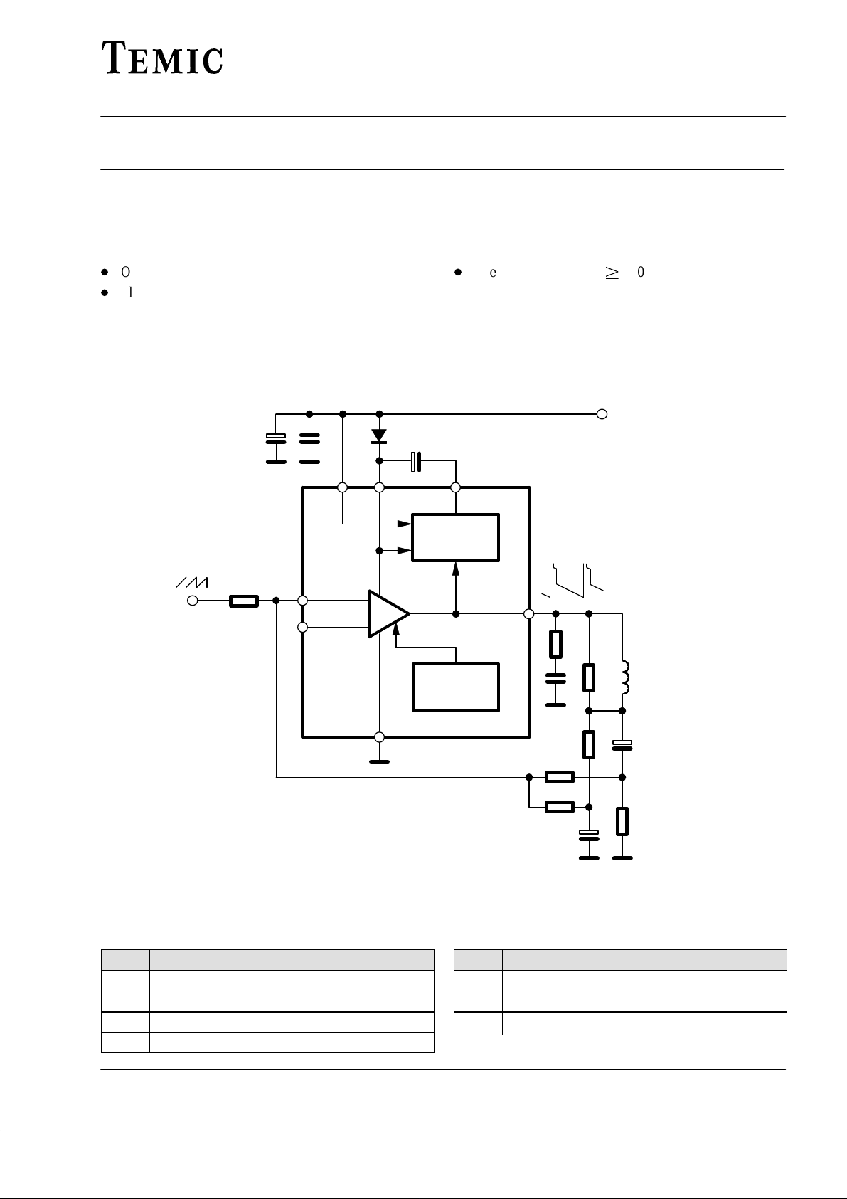
Block diagram
6
23
D
Thermal protection, Tj 140°C
+ V
TEA 8172
S
94 8723
Pin Configuration
1
Power
amplifier
–
7
+
4
Figure 1 Block diagram
Flyback
generator
Thermal
protection
5
Deflection
coil
Pin Function
1 Inverted input
2 Supply voltage
3 Flyback generator
4 Ground
Rev . A1: 17.07.1995
Pin Function
5 Output
6 Output stage supply
7
Non inverted input
1
TEA 8172
Absolute Maximum Ratings
Parameters Symbol Value Unit
Supply voltage Pin 2 V
Flyback peak voltage Pins 5 and 6 V
Voltage at pin 3 V
Input voltage Pins 1 and 7 V
Output peak current: Pin 5
t = 2 ms, non repetitive
f = 50/60 Hz, t v10 ms
f = 50/60 Hz, t > 10 ms
DC current at pin 3, V
Flyback current peak to peak, Pin 3
f= 50/60 Hz, t
Power dissipation, T
Storage temperature T
Junction temperature T
V
5 <
2
≤ 1.5 ms
fly
= 70°C P
case
I
I
I
S
5, 6
3
1, 7
O
3
3
tot
stg
j
TELEFUNKEN Semiconductors
35 V
60 V
V
S
V
S
2.5
3.0
2.0
100 mA
3 A
20 W
– 40 to + 150 °C
– 40 to + 150 °C
V
V
A
Thermal Resistance
Parameters Symbol Maximum Unit
Junction case R
Electrical Characteristics
V
= 35 V, T
S
Quiescent current I3 = 0, I
Input quiescent current V
Saturation voltage to GND I
Output voltage V
Saturation voltage to GND I5 = 0.7 A Pin 5
Saturation voltage to
supply
Junction temperature for
thermal shut down
= 25°C, reference point Pin 4 (GND), see test circuits, unless otherwise specified
amb
Parameters Test Conditions / Pin Symbol Min Typ Max Unit
I
= 0, I
3
0 Pin 2
S =
0 Pin 6
S =
I
I
figure 2
= 1 V Pin 1
1
–I
figure 3
= 20 mA Pin 3
3
V
figure 4
= 35 V, R
S
= 39 k
r
W
V
figure 5 Pin 5
V
I
= 1.2 A
5
figure 6
I5 = – 0.7 A Pin 5
I
= – 1.2 A
5
V
figure 7
T
2
6
3-4
5-4
5-6
thJC
1
3 K/W
8
16
16
36
0.1 1
mA
m
A
1 1.5 V
5
j
18 V
0.7
1.0
1.3
1.6
1.0
1.4
1.8
2.2
V
V
140 °C
2
Rev . A1: 17.07.1995
 Loading...