

TEMIC TDA4472-MSD, TDA4472-MFLG3 Datasheet
TDA4472-M
Video-IF and Quasi Parallel Sound Processing
Description
The TDA4472 is an integrated bipolar circuit for video/
sound IF (VIF/SIF) signal processing in TV/VCR and
multimedia applications. The circuit processes all TV
Features
D
5 V supply voltage; low power consumption
D
Active carrier generation by FPLL principle
(frequency-phase-locked-loop) for true
synchronous demodulation
D
Very linear video demodulation, good pulse response
and excellent intermodulation figures
D
VCO circuit operates at picture carrier frequency
D
Alignment-free AFC without external reference
circuit, polarity of the AFC curve is switchable
video IF signals with negative modulation (e.g., B/G
standard), and the FM/NICAM sound IF signals.
D
Alignment-free quasi parallel sound (QPS) mixer for
FM/NICAM sound IF signals
D
Intercarrier output signal is gain controlled (necessary
for digital sound processing)
D
Separate SIF-AGC with average detection
D
Two independent SIF inputs
D
Package and relevant pinning is compatible with the
multistandard version TDA4470, which simplifies the
design of an universal IF module
D
VIF-AGC with peak sync. detection
D
Tuner AGC with adjustable take over point
Package: SDIP28, SO28
Ordering Information
Extended Type Number Package Remarks
TDA4472-MSD SDIP28
TDA4472-MFLG3 SO28 Delivery in taped form
TELEFUNKEN Semiconductors
Rev . A2, 15-Oct-96
1 (14)
Preliminary Information
TDA4472-M
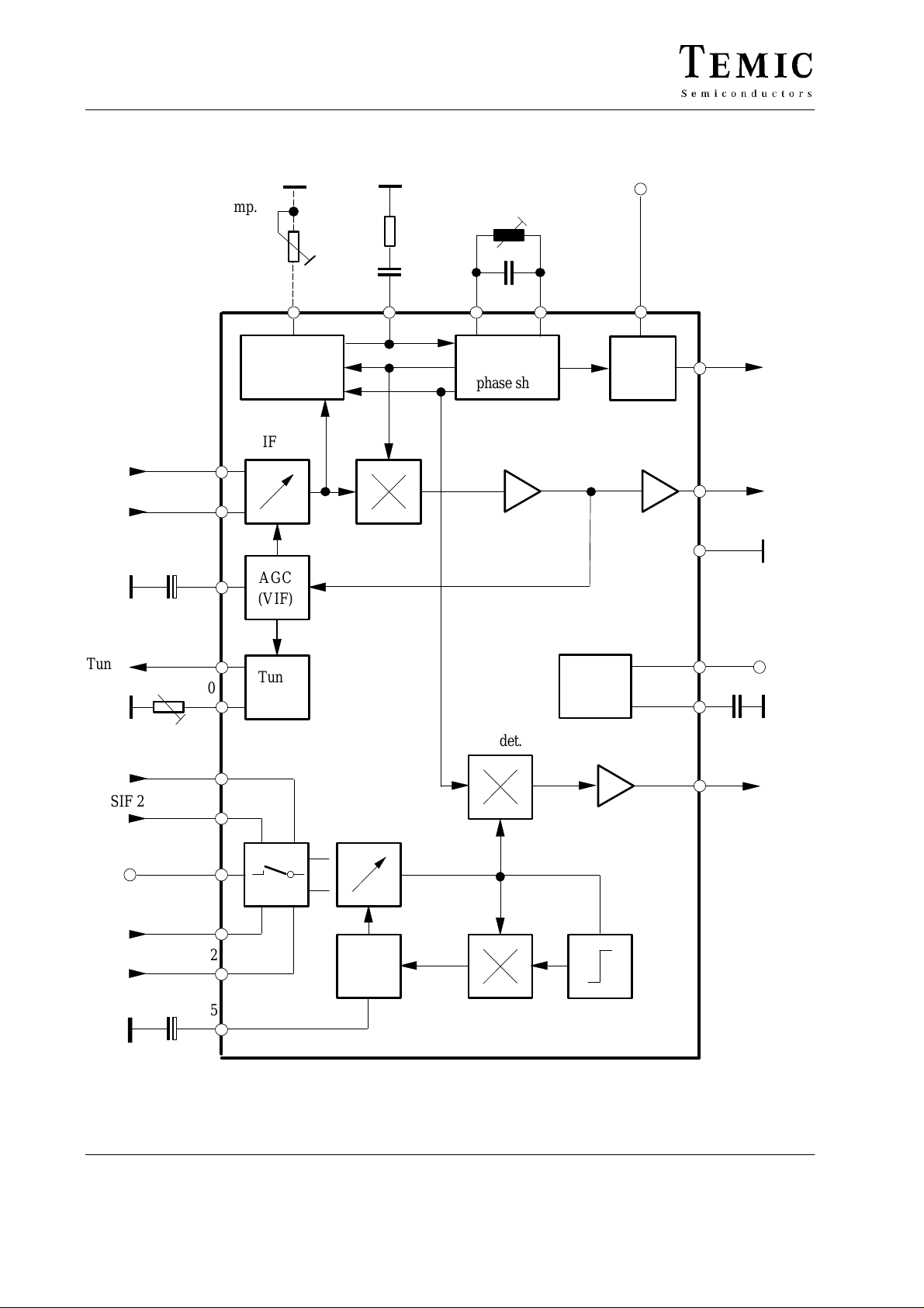
Block Diagram
VIF
C
AGC
Offset
comp.
(optional)
VIF amp
6
7
8
26
FPL
L
AGC
(VIF)
Loop
filter
Video
det.
18
0°
90°
VCO
2 0
phase shift
VCO
+
21
AFC
AFC
switch
19
22
12
4,9,16
AFC
Video
Tuner
Take over point
SIF 2
Input switch
SIF 1
C
AGC
11
10
27
28
23
Tuner
AGC
FM det.
SIF amp
3
1
2
5
AGC
(SIF)
Supply
17
C
24
(FM / NICAM)
94 8719
V
S
Ref
Intercarrier
2 (14)
Figure 1. Block diagram
TELEFUNKEN Semiconductors
Rev . A2, 15-Oct-96
Preliminary Information

Circuit Description
Vision IF Amplifier
The video IF signal (VIF) is fed through a SAW filter to
the differential input (Pin 6-7) of the VIF amplifier. This
amplifier consists of three AC-coupled amplifier stages.
Each differential amplifier is gain controlled by the automatic gain control (VIF-AGC). The output signal of the
VIF amplifier is applied to the FPLL carrier generation
and the video demodulator.
Tuner-and VIF-AGC
At Pin 8, the VIF-AGC charges/discharges the AGC
capacitor to generate a control voltage for setting the gain
of the VIF amplifier and tuner in order to keep the video
output signal at a constant level. Therefore, in the case of
all negative modulated signals (e.g., B/G standard) the
sync. level of the demodulated video signal is the
criterion for a fast charge/discharge of the AGC capacitor .
The control voltage (AGC voltage at Pin 8) is transferred
to an internal control signal, and is fed to the tuner AGC
to generate the tuner AGC current at Pin 11 (open
collector output). The take over point of the tuner AGC
can be adjusted at Pin 10 by a potentiometer or an external
dc voltage (from interface circuit or microprocessor).
TDA4472-M
designed for low distortion and large bandwidth. The
demodulator output signal passes an integrated low pass
filter for attenuation of the residual vision carrier and is
fed to the video amplifier. The video amplifier is realized
by an operational amplifier with internal feedback and
8 MHz bandwidth (–3 dB). An additional noise clipping
is provided. The video signal is fed to VIF-AGC and to the
video output buffer . This amplifier with a 6 dB gain offers
easy adaption of the sound trap. For nominal video IF
modulation the video output signal at Pin 12 is 2 V
Sound IF Amplifier and SIF-AGC
The SIF amplifier is nearly identical with the 3-stage VIF
amplifier. Only the first amplifier stage exists twice and
is switchable by a control voltage at Pin 3. Therefore with
a minimal external expense it is possible to switch
between two different SAW filters. Both SIF inputs
features excellent cross-talk attenuation and an input
impedance which is independent from the switching
condition.
The SIF-AGC is related to the average level of FM-carrier
and controls the SIF amplifier to provide a constant SIF
signal to the QPS mixer.
pp.
FPLL, VCO and AFC
The FPLL circuit (frequency phase locked loop) consists
of a frequency and phase detector to generate the control
voltage for the VCO tuning. In the locked mode, the VCO
is controlled by the phase detector and in unlocked mode,
the frequency detector is superimposed. The VCO
operates with an external resonance circuit (L and C parallel) and is controlled by internal varicaps. The VCO
control voltage is also converted to a current and represents the AFC output signal at Pin 22.
A practicable VCO alignment of the external coil is the
adjustment to zero AFC output current at Pin 22. At center
frequency the AFC output current is equal to zero.
The optional potentiometer at Pin 26 allows an offset
compensation of the VCO phase for improved sound
quality (fine adjustment). Without a potentiometer (open
circuit at Pin 26), this offset compensation is not active.
The oscillator signal passes a phase shifter and supplies
the in-phase signal (0°) and the quadrature signal (90°)of
the generated picture carrier.
Video Demodulation and Amplifier
The video IF signal, which is applied from the gain
controlled IF amplifier, is multiplied with the inphase
component of the VCO signal. The video demodulator is
Quasi-Parallel-Sound (QPS) Mixer
The QPS mixer is realized by a multiplier. The SIF signal
(FM or NICAM carrier) is converted to the intercarrier
frequency by the regenerated picture carrier (quadrature
signal) which is provided from the VCO. The intercarrier
signal is fed via an output amplifier to Pin 24.
AFC Switch
The AFC output signal at Pin 22 can be controlled by a
switching voltage at Pin 19. It is possible to switch off the
AFC.
VCR Mode
For the VCR mode in a TV set (external video source
selected), it is recommendable to switch off the IF circuit.
With an external switching voltage at Pin 6 or 7, the IF
amplifiers are switched off and all signal output levels at
Pins 12 and 24 are according to the internal dc voltage.
Internal Voltage Stabilizer
The internal bandgap reference ensures constant performance independent of supply voltage and temperature.
TELEFUNKEN Semiconductors
Rev . A2, 15-Oct-96
3 (14)
Preliminary Information
TDA4472-M
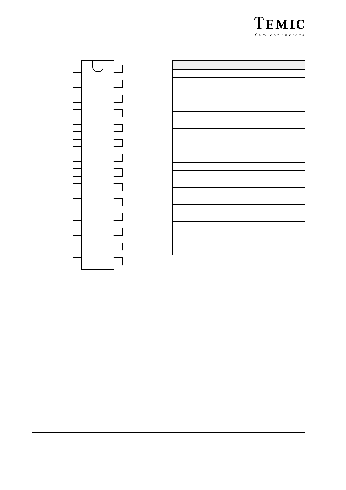
Pin Description
V
i,SIF1
V
i,SIF1
V
GND
C
V
i,VIF
V
i,VIF
C
GND
R
I
V
o,vid
NC
SW
AGC
AGC
top
tun
NC
1
2
3
4
5
6
7
8
9
10
11
12
13
14
94 8835
Figure 2. Pinning
28
27
26
25
24
23
22
21
20
19
18
17
16
15
V
i,SIF2
V
i,SIF2
R
comp
NC
V
o,FM
V
S
V
AFC
V
VCO
V
VCO
Vsw
LF
C
ref
GND
NC
Pin Symbol Function
1, 2 Vi,
3 V
SIF1 input (symmetrical)
SIF1
Input selector switch
sw
4, 9, 16 GND Ground
5 C
6, 7 V
8 C
10 R
11 I
12 V
AGC
i, VIF
AGC
top
tun
o,vid
SIF-AGC (time constant)
VIF input (symmetrical)
VIF-AGC (time constant)
Take over point, tuner AGC
Tuner AGC output current
Video output
13 NC Not connected
14 NC Not connected
15 NC Not connected
17 C
Internal reference voltage
ref
18 LF Loop filter
19 V
20, 21 V
22 V
23 V
24 VO,
VCO
AFC
AFC switch
sw
VCO circuit
AFC output
Supply voltage
S
Intercarrier output
FM
25 NC Not connected
26 R
27, 28 V
comp
i, SIF2
Offset compensation
SIF 2 input (symmetrical)
4 (14)
TELEFUNKEN Semiconductors
Rev . A2, 15-Oct-96
Preliminary Information
Absolute Maximum Ratings
Reference point Pin 4 (9, 16), unless otherwise specified
Parameters Symbol Value Unit
Supply voltage Pin 23
SDIP28 package
SO28 package
Supply current Pin 23 I
Power dissipation SDIP28 package
SO28 package
Output currents Pins 12 and 24 I
External voltages
Pins 1, 2, 5 to 8, 10, 12, 17, 18 and 24, 26 to 28
Pins 20 and 21
Pin 11
Pins 3, 19 and 22
Junction temperature T
Storage temperature T
Electrostatic handling *) all pins V
*)
Equivalent to discharging a 200 pF capacitor trough a 0 W resistor.
V
V
V
S
S
s
P
P
out
ext
j
stg
ESD
TDA4472-M
9.0
6.0
93 mA
840
560
5 mA
+4.5
+3.5
+13.5
V
S
+125 °C
–25 to +125 °C
"
300
V
V
mW
mW
V
V
V
V
V
Operating Range
Parameters Symbol Value Unit
Supply voltage range Pin 23
SDIP28 package
SO28 package
Ambient temperature T
Thermal Resistance
Parameters Symbol Maximum Unit
Junction ambient, when soldered to PCB
SDIP28 package
SO28 package
R
R
V
V
amb
thJA
thJA
S
S
4.5 to 9.0
4.5 to 6.0
–10 to +85 °C
55
75
V
V
K/W
K/W
TELEFUNKEN Semiconductors
Rev . A2, 15-Oct-96
5 (14)
Preliminary Information
 Loading...