

TEMIC TDA4453 Datasheet
TDA4453
Video IF Amplifier for Multistandard TV Receiver and VTR
Appliances
Technology: Bipolar
Features
D
Interference suppression
D
Standard B/G-L suitable, processes negatively and
positively modulated IF-signals with equal polarity of
the output signal
D
Ultra white inverter and ultra black limiter for
reducing transmission interference
D
Internally noise protected gain control, no flyback
pulses required
D
Expanded video frequency response allows the
demodulation of amplitude modulated MAC signals
D
High input sensitivity
D
Minimal intermodulation interference
D
Fast AGC by controlled discharge of the
AGC capacitor
Standard L mode: AGC acting on peak white level,
capacitor discharge control by averaged video signal
Standard B/G: AGC acting on the sync. pulse peak
D
Small differential error
D
Constant input impedance
D
Video output voltage with narrow tolerance
D
Adapted output for insertion of ceramic transducers as
intrinsic sound trap
D
Connecting and basic circuitry compatible to the
TEMIC video IF type programme - permits building
block system for video IF module
TELEFUNKEN Semiconductors
Rev . A1, 15-Aug-96
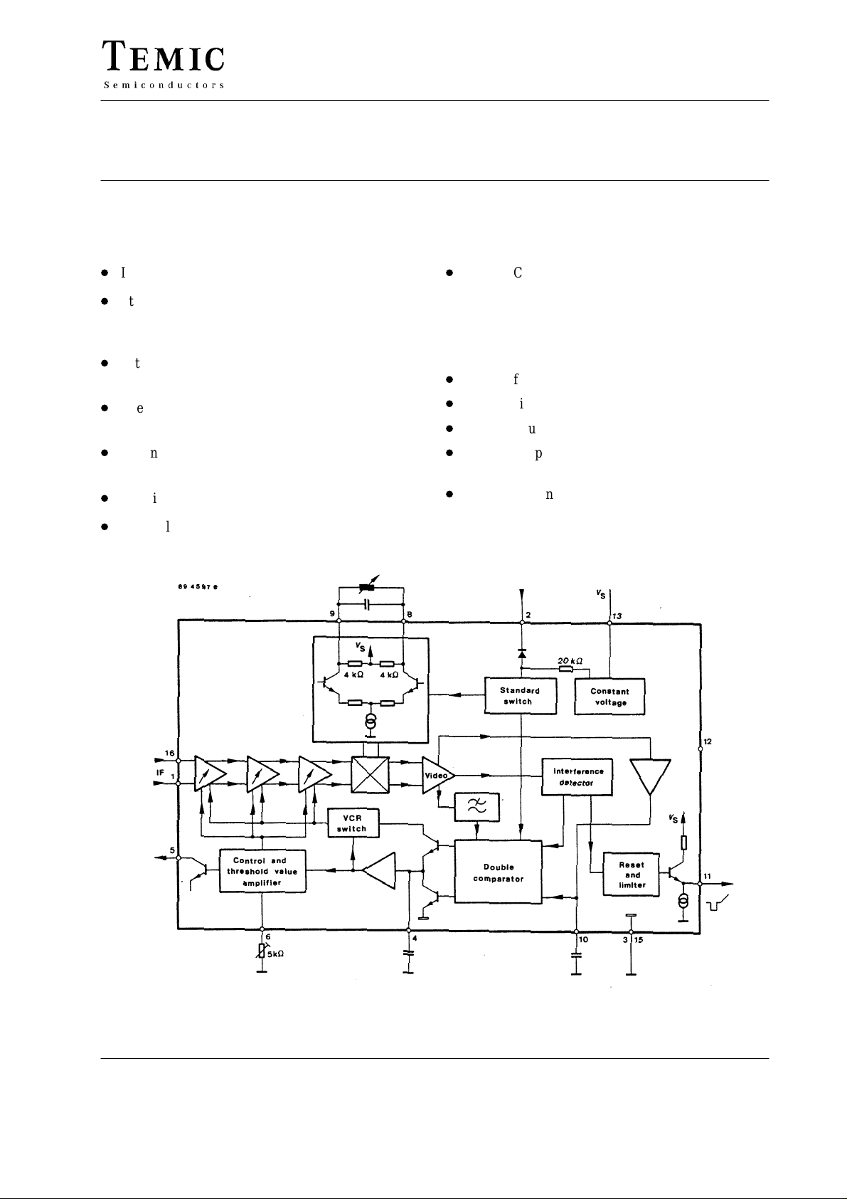
Figure 1. Block diagram
1 (7)
TDA4453
Pin Description
Pin Function
1,16 IF-input
2 Standard switch: open B/G
ground L
3,15 Ground
4 IF-AGC storage capacitor
5 AGC (tuner control)
6 Tuner AGC take over
Circuit Description
The following function units are integrated in this circuit
combination for video-IF processing:
D
Three symmetric, highly stable, gain controlled wideband amplifier, quasi galvanic coupling eliminates
feed back
D
Video carrier controlled demodulator of high linearity
D
Polarity switch over for video
Pin Function
7 Not connected
8,9 Demodulator circuit
10 Average capacitor standard L
11 Video output
12 Not connected
13 Supply voltage
14 Not connected
D
Video output amplifier with low-pass characteristics,
limiter for ultra black and inverter for ultra white
interference
D
High impedance, interference free controlled voltage
facilities, best possible AGC time constant with small
storage capacitor
D
Controlled discharge circuit for fast gain control
D
With VTR - operation the video output level is
according to the ultra white level in B/G, ultra black
level in L
Absolute Maximum Ratings
Reference point Pin 3, unless otherwise specified
Parameters Symbol Value Unit
Supply voltage Pin 13 V
Supply current Pin 13 I
Open loop voltage Pin 5 V
External voltage Pin 4
Pin 11
Breaking current for VTR operation Pin 4 I
Video output current
Max. load Pin 11
Short circuit max 1 s Pin 11
Power dissipation T
Junction temperature T
Ambient temperature range T
Storage temperature range T
≤ 60°C P
amb
Thermal Resistance
Parameters Symbol Maximum Unit
Junction ambient R
V
V
I
amb
thJA
O
tot
stg
S
S
5
4
11
4
j
10 to 13.5 V
65 mA
V
S
10
8
0.3 mA
5
30
1.0 W
125 °C
–25 to +70 °C
–25 to +125 °C
60 K/W
V
V
mA
2 (7)
TELEFUNKEN Semiconductors
Rev . A1, 15-Aug-96
TDA4453
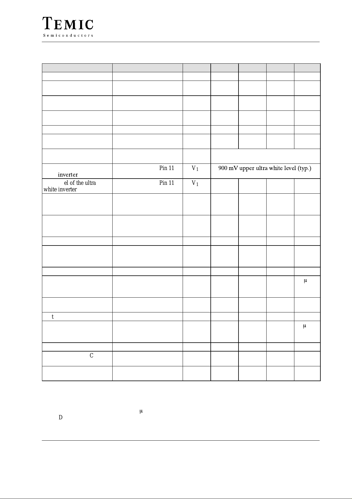
Electrical Characteristics
Parameters Test Conditions / Pins Symbol Min. Typ. Max. Unit
Supply current Pin 13 I
Ultra white level at
1)
Pin 11 V
S
o
4.8 5.2 5.6 V
standard B/G
Ultra black clamping level
Pin 11 V
o
1.75 1.9 2.05 V
at standard B?G
Composite video output
2)
Pin 11 v
o(pp)
2.7 3.0 3.3 V
signal B/G
Video signal standard L 3)(black/white) Pin 11 v
Difference of the video
Pin 11 10 %
o(pp)
1.85 2.1 2.35 V
signals standard L-B/G
Clamping level of black
Pin 11 V
11
limiter
Threshold of the ultra
white
Grey level of the ultra
Pin 11 V
Pin 11 V
11
11
white inverter
Supply voltage influence
Pin 11 ∆V
black
on the ultra black level in
standard B/G
Supply voltage influence
Pin 11 ∆V
white
on the ultra white level in
standard B/G
Video bandwidth (–3 dB) Pin 11 B
Video frequency response
Pin 11 ∆V
Video
Video
over the AGC control
range
Output DC current V11= 8 V Pin 11 I
Response time of the
4)
Pin 4 t
11
r
peak white control in
standard L
Voltage level standard
5)
Pin 2 V
2
2 V
B/G
Voltage level standard L
Input sensitivity
6)
(symmetrical)
5)
v
=3.0 V Pin
14(pp)
Pin 2 V
2
v
i
0 1.2 V
1–16
V
= 0.8 V
4
IF-AGC gain reduction ∆P 60 dB
Available tuner AGC 10 dB via AGC use
I
5
3 4 mA
Pin 5
Automatic tuner AGC with
IF-control
Pin 6 not connected
Pin 5
AGC 61 dB
65 mA
250 mV below sync. (typ.)
3.6 V
0.5 %/V
1.0 %/V
10 MHz
2.0 dB
2.8 mA
10
S
100
m
s
V
m
V
1)
All measurements Pin 11 without load
2)
Residual carrier 10%
3)
Blanking level 30% carrier amplitude
4)
A peak white value for at least 10 ms must be transmitted for each complete frame
5
) Direct control of standard reversing switch with TTL level
6)
Sync. peak value standard B/G
TELEFUNKEN Semiconductors
Rev . A1, 15-Aug-96
3 (7)
 Loading...