

TEMIC TDA4445A, TDA4445B Datasheet
TELEFUNKEN Semiconductors
TDA4445A/TDA4445B
Quasi Parallel Sound Processing with Quadrature
Intercarrier Demodulator
Technology: Bipolar
Features
D
Very high input sensitivity
D
Excellent signal to noise ratio
D
Fast averaged AGC
D
IF amplifier can be switched off for VTR mode
D
Output signal stabilized against V
D
Very few external components
variations
S
TDA4445B additional
D
Targeting bistandard applications (B/G and L)
D
Alignment free AM demodulator
D
Low AM distortion
Case: DIP16
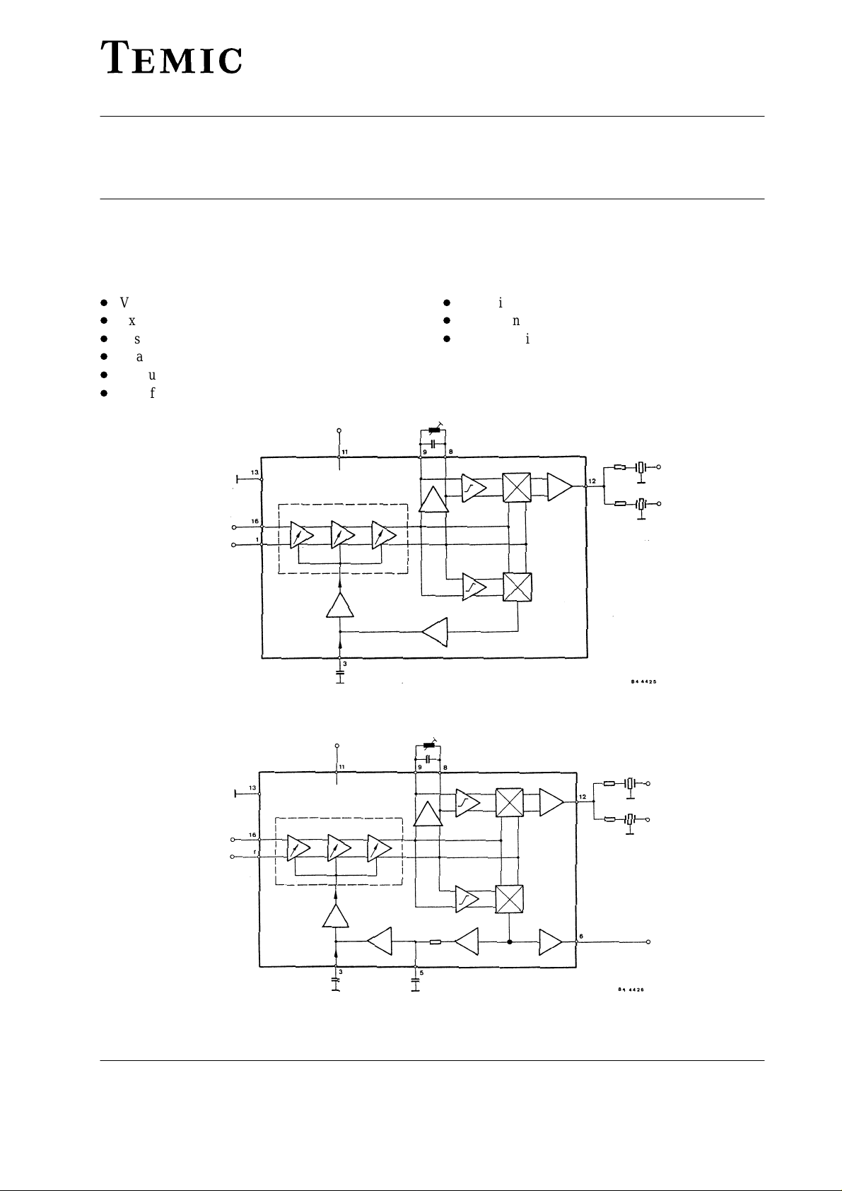
Figure 1. Block diagram TDA4445A
Figure 2. Block diagram TDA4445B
Rev . A1: 14.09.1995 1 (8)
TDA4445A/TDA4445B
TELEFUNKEN Semiconductors
Pin Description
Pin Symbol Function
1–16 IF input
3 If AGC time constant
8–9 Tuned circuit
11 Supply voltage
12 Sound-IF-output
13 Ground
2, 4,
7, 10,
14, 15
not connected
TDA4445B additional
Pin Symbol Function
5 Average capacitor
6 AF output
Circuit Description
This circuit includes the following functions
D
Three symmetrical and gain controlled wide band
amplifier stages, which are extremely stable by quasi
DC coupling without feedback
D
Averaged AGC with discharge control circuit
D
AGC voltage generator
Quasi parallel sound operation
D
High phase accuracy of the carrier signal processing,
independent from AM
D
Linear quadrature demodulator
D
Sound–IF–amplifier stage with impedance converter
AM–Demodulation (TDA4445B only)
D
Carrier controlled demodulator
D
Audio frequency stage with impedance converter
D
Averaged low pass AGC
Absolute Maximum Ratings
Reference point pin 3, unless otherwise specified
Parameters Symbol Value Unit
Supply voltage range Pin 11 V
Supply current Pin 11 I
External voltages
TDA4445A, B Pin 3
Pin 12
TDA4445B only Pin 5, 6
Power dissipation in soldered position P
Junction temperature T
Ambient temperature range T
Storage temperature range T
Thermal Resistance
Parameters Symbol Value Unit
Junction ambient R
V
S
S
ext
tot
j
amb
stg
thJA
10 ... 15 V
70 mA
12
8
8
1 W
125 °C
–25 to +70 °C
–25 to +125 °C
60 K/W
V
Rev . A1: 14.09.19952 (8)
TELEFUNKEN Semiconductors
i
TDA4445A/TDA4445B
Electrical Characteristics
V
= 12 V, T
S
= + 25°C, reference point pin 13, unless otherwise specified
amb
Parameters Test Conditions / Pins Symbol Min. Typ. Max. Unit
Supply current V
DC output voltage V
= 10 mV
1–16
or V
= 3.5 V Pin 11
3
= 10 mV,
1–16
I
S
V
O
60 mA
5.0 V
unmodulated Pin 12
DC output current V11 = 7.5 V,
V
= 3.5 V Pin 12 I
3
Input impedance Pin 1–16
Pin 1–16
max
R
C
1.8 V
1.6
2.0
Switch off control voltage VTR mode Pin 3 V 8 10 V
Switch off control current VTR mode Pin 3 I 50 150
Quasi Parallel Sound Operation
k
PF
m
W
A
fPC = 38.9 MHz, f
= 33.4 MHz, f
SC1
= 33.16 MHz, PC/SC = 13 dB, PC/SC2 = 20 dB,
SC2
PC unmodulated (equivalent to sync. peak current)
Parameters Test Conditions / Pins Symbol Min. Typ. Max. Unit
Minimum input voltage 5.5 MHz output signal
–3dB Pin 1–16
Maximum input voltage 5.5 MHz output signal
+1 dB Pin 1–16
IF AGC range ∆G
AGC capacitor control time constant, Pin 3 C
Sound-IF-output voltage V
5.5 MHz output voltage
= 10 mV, SC unmodulated
1–16
Pin 12 v
5.74 MHz output voltage
Signal to noise ratio: measured according to CCIR 468–2
reference signal: v
f
= 1 kHz, measured at audio-output sound IF demodulator U2829B
mod
1. Channel/ 2. Channel
Standard B/G modulated IF signal
(residual carrier 10%)
= 10 mV, FM-frequency deviation = +30 kHz
1–16
Black screen Pin 12
Grid pattern
Bistandard Operation
Parameters Test Conditions / Pins Symbol Min. Typ. Max. Unit
IF AGC range ∆
AGC capacitor
(control time constant)
Pin 3
Pin 5
v
i
v
i
3
i
S+N
N
G
IF
C
3
C
5
50
m
V
80 mV
IF
0.33 10
64 dB
250
m
mV
F
110
62/58
dB
52/49
64 dB
10
m
F
4.7
Rev . A1: 14.09.1995 3 (8)
 Loading...