

TEMIC TDA4439 Datasheet
TELEFUNKEN Semiconductors
TDA4439
Video IF Amplifier for Multistandard TV and VTR
Technology: Bipolar
Features
D
Standard B/G-L suitable, processes negatively and
positively modulated IF-signals with equal polarity of
the output signal
D
Ultra white inverter and ultra black limiter for reducing transmission interference
D
Internally noise protected gain control, no flyback
pulses required
D
Expanded video frequency response allows the demodulation of amplitude modulated MAC signals
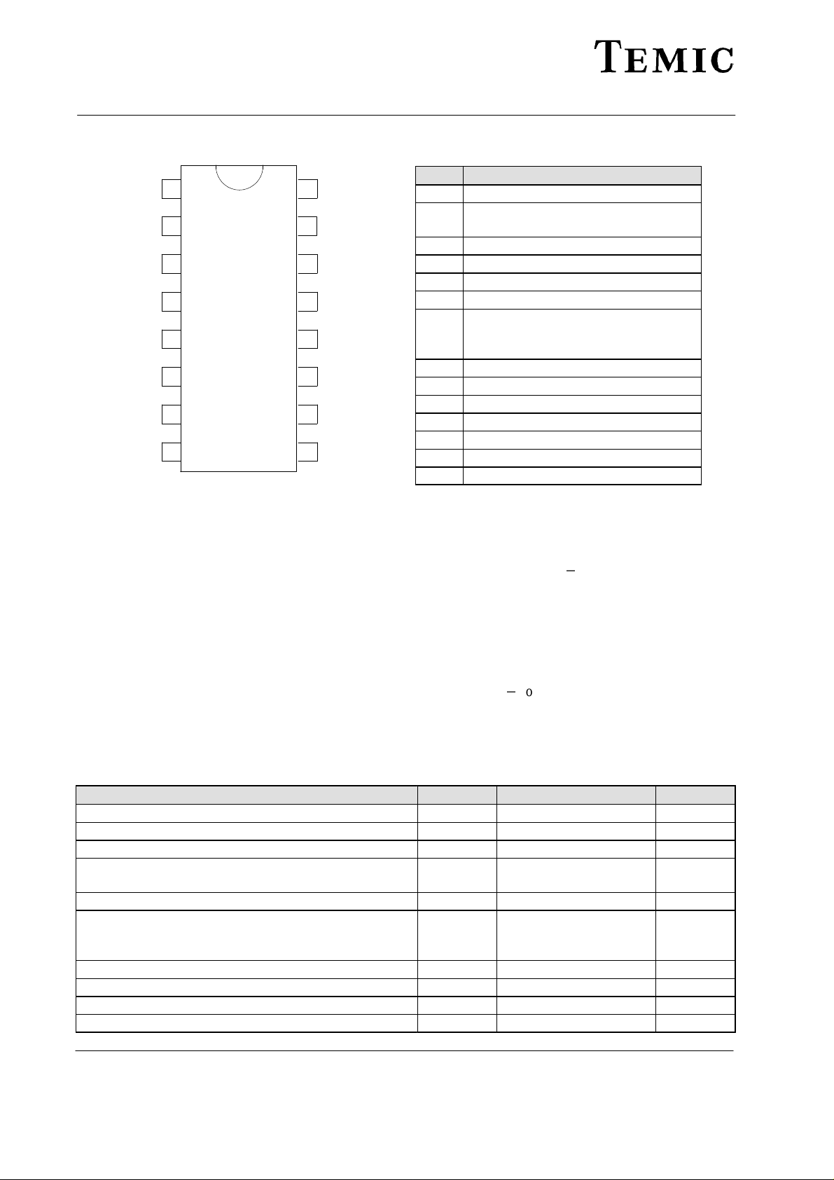
Case: DIP18
D
High input sensitivity
D
Fast AGC by controlled discharge of the AGC capacitor
Standard L mode: AGC acting on peak white level,
capacitor discharge control by averaged video signal
Standard B/G: AGC acting on the sync. pulse peak
D
The direction of the AFC curve is selectable independently from the standard switch
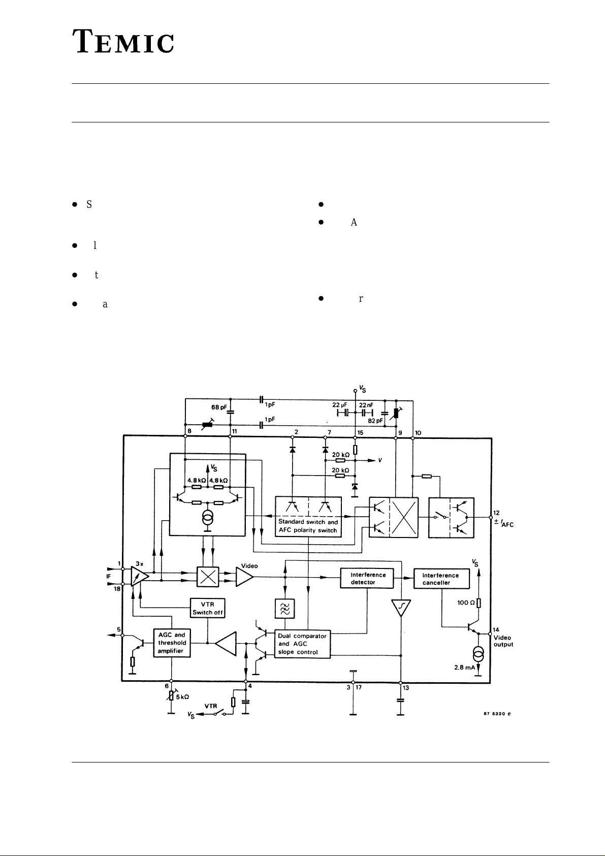
Figure 1. Block diagram
Rev . A1: 14.09.1995 1 (7)
TDA4439
Pin Description
TELEFUNKEN Semiconductors
1
16
1, 18 IF input
2 Standard switch: open B/G
Pin Function
2
15
ground L
3, 17 Ground
3
14
4 IF-AGC storage capacitor
5 AGC (tuner control)
4
13
6 Tuner AGC take over
7 Polarity switch:
5
6
12
11
8, 11 Demodulator circuit
9, 10 AFC circuit
open AFC “DOWN”
ground AFC
“UP”
12 AFC output
7
10
13 Average capacitor standard L
14 Video output
8
95 10840
9
15 Supply voltage
16 n.c.
Circuit Description
The following function units are integrated in this circuit combination for video-IF processing:
– Three symmetric, highly stable, gain controlled wide-
band amplifier, quasi galvanic coupling eliminates
feed back
– Video carrier controlled demodulator of high linearity
– Polarity switch over for video and AFC-signal
– Video output amplifier with low-pass characteristics,
limiter for ultra black and inverter for ultra white
interference
– Disconnectable AFC * generator with push pull
current output
– High impedance, interference free controlled voltage
facilities, best possible AGC time constant with small
storage capacitor
– Controlled discharge circuit for fast gain control
– With VTR * operation the video output level is
according to the ultra white level in B/G, ultra black
level in L
Absolute Maximum Ratings
Reference point pin 3, unless otherwise specified
Parameters Symbol Value Unit
Supply voltage Pin 15 V
Supply current Pin 15 I
Open loop voltage Pin 5 V
External voltage Pin 4
Pin 14
Breaking current for VTR operation Pin 4 I
Video output current
max load Pin 14
short circuit max 1 s Pin 14
Power dissipation T
Junction temperature T
Ambient temperature range T
Storage temperature range T
≤ 60°C P
amb
V
V
I
tot
amb
stg
S
14
4
0
S
10 to 15 V
75 mA
5
4
V
10
S
8
V
V
V
0.5 mA
5
mA
50
1.0 W
j
125 °C
–25 to +70 °C
–25 to +125 °C
Rev . A1: 14.09.19952 (7)
TELEFUNKEN Semiconductors
Thermal Resistance
Parameters Symbol Maximum Unit
Junction ambient R
Electrical Characteristics
thJA
TDA4439
60 K/W
V
= 12 V, T
S
= 25°C, Reference point Pin 3, unless otherwise specified
amb
Parameters Test Conditions / Pins Symbol Min. Typ. Max. Unit
Supply current Pin 15 I
Ultra white level at
1)
standard B/G Pin 14 v
Ultra black clamping level
at standard B/G
Composite video output
2)
Pin 14 v
signal B/G Peak to peak Pin 14 v
Video signal standard L
3)
(black/white) Peak to peak Pin 14 v
Difference of the video
signals
standard L-B/G
Pin 14 ∆ 10 %
Clamping level of black
limiter
Pin 14 V
Threshold of the ultra white
inverter
Pin 14 V
Grey level of the ultra white
inverter
Pin 14 V
Supply voltage influence on
the ultra black level in
standard B/G
Pin 14 ∆ 0.5 %/V
Supply voltage influence on
the ultra white level in
standard B/G
Pin 14 ∆ 1.0 %/V
Video bandwidth –3 dB Pin 14 B
Video frequency response
over the AGC control range
Output DC current
Response time of the peak
V
= 8 V Pin 14
14
4)
Pin 14 ∆V
white control in standard L Pin 4 t
Voltage level standard B/G
Voltage level standard L
Input sensitivity (sym.)
5)
5)
6)
v14=3.0 Vpp,
= 0.8 V Pin 1–18 v
V
4
Pin 2 V
Pin 2 V
IF-AGC gain reduction ∆v
Available tuner AGC
10 dB via AGC use
Pin 5 I
Automatic tuner AGC with
IF-control Pin 6 n.c.
Pin 5 AGC 61 dB
S
0
0
0
0
14
14
14
video
video
I
14
r
2
2
i
p
5
65 mA
4.8 5.2 5.6 V
1.75 1.9 2.05 V
2.7 3.0 3.3 V
1.85 2.1 2.35 V
250 mV below Sync. (typ.)
900 mV upper ultra white level (typ.)
3.6 V
10 MHz
2.0 dB
2.8 mA
2 V
10
S
m
0 1.2 V
120
m
60 dB
3 4 mA
s
V
V
Rev . A1: 14.09.1995 3 (7)
 Loading...