

TEMIC TDA1083 Datasheet
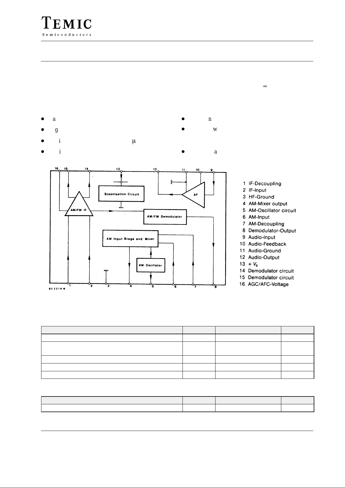
TDA1083
One Chip AM/FM Radio with Audio Power Amplifier
Description
The integrated circuit TDA1083 includes, with exception
of the FM front end, a complete AM-/FM-radio-circuit
with audio power amplifier. An internal Z-diode
Features
D
Large supply voltage range V
D
High AM-Sensitivity
= 3 to 12 V
S
stabilizes the supply voltage at V
with the aid of a resistor and a rectifier, the circuit to be
driven by a higher external supply voltage.
D
AFC-connection for VHF-tuner
D
AM-FM switching without high frequency voltages
[
13 V, which allows
S
D
Limiting threshold voltage V
D
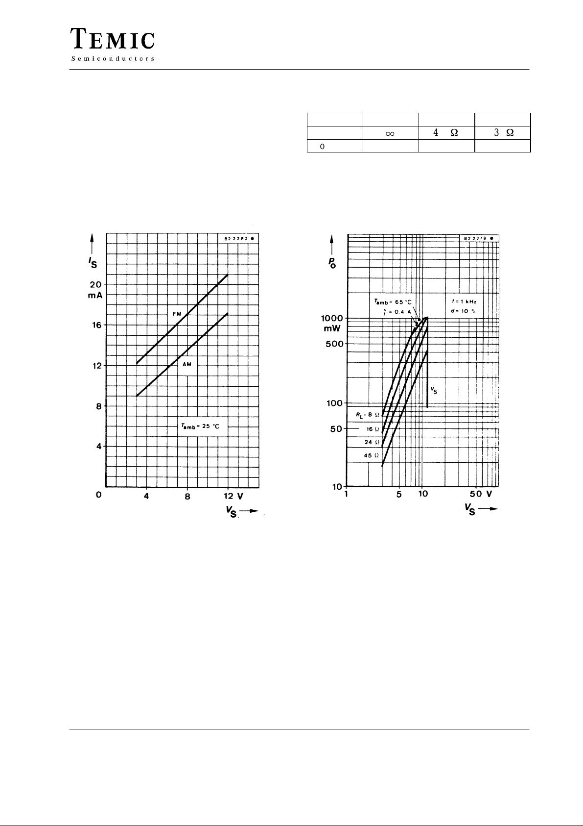
Audio output power P
i
0 = 0.7 W
= 50 mV
Figure 1. Block diagram and pin connections
Applications
D
AM-/FM- and audio-amplifier
Absolute Maximum Ratings
Reference points Pin 3 and 11, unless otherwise specified
Parameters Symbol Value Unit
Supply voltage range Pin 13 V
Supply current when using the integrated stabilization
circuit, V
Power dissipation T
Junction temperature T
Storage temperature range T
= 12.5 to 14.3 V Pin 13 I
S
= 65°C P
amb
Thermal Resistance
Parameters Symbol Maximum Unit
Junction ambient R
TELEFUNKEN Semiconductors
Rev . A1, 17-Jun-96
s
S
tot
j
stg
thJA
3 to 12 V
50 mA
600 mW
125 °C
–25 to +125 °C
100 K/W
1 (10)
TDA1083
Electrical Characteristics
V
= 9 V, reference points Pin 3 and 11, T
s
= 25°C, unless otherwise specified
amb
Parameters Test Conditions / Pin Symbol Min Typ Max Unit
AF amplifier
AF voltage amplification f = 1 kHz G
Input impedance R
Output power Figures 4 and 5
V
= 5.5 V,
S
R
= 8 W, k = 10%
L
AM-IF amplifier, f
= 1 MHz, f
i
DC voltages at AM mode
without signal
= 455 kHz, f
IF
V
= 3 V Pin 10
S
= 1 kHz, m = 0.3
mod
Pin 12
Pin 13
Pin 16
I
= 42 mA Pin 10
S
(V
= 12.5 to14.3 V)
S
Pin 12
Pin 13
Pin 16
Regulation range V
oAF/VoAF
= –10 dB
Pin 6
AF voltage at demodulator
Pin 8 V
output
FM-IF amplifier, f
= 10.7 MHz, Df = "22.5 kHz, f
IF
DC voltages at FM mode
without signal
V
= 3 V Pin 10
S
mod
Pin 12
= 1 kHz
Pin 13
Pin 16
V
V
V
V
V
V
V
V
D
V
V
V
V
P
10
12
13
16
10
12
13
16
V
oAF
10
12
13
16
v
i
o
300 mW
1.0
3.0
1.25
40 dB
150 k
1.2
1.4
3.0
3.0
2.0
1.2
7.2
W
V
V
V
V
V
V
5.9
12.5
13.3
1.5
i
70 dB
14.3
2.0
V
V
100 mV
1.0
3.0
1.8
1.2
3.0
1.4
3.0
2.8
V
V
V
V
I
= 42 mA Pin 10
S
(V
= 12.5 to 14.3 V)
S
Pin 12
Pin 13
Pin 16
V
V
V
V
Limiting threshold (–3 dB) Pin 2 V
AF voltage at demodulator
Pin 8 V
output
2 (10)
10
12
13
16
oAF
1.2
7.2
V
V
5.9
12.5
13.3
2.0
i
50
14.3
3.1
V
V
m
V
100 mV
TELEFUNKEN Semiconductors
Rev . A1, 17-Jun-96
TDA1083
Different dc voltages are developed at Pin 16 due to gain
spread of AM-IF-amplifier. To determine the value of
parallel resistance R
Pin 8 for V
should be selected at Pin 16.
= 9 V, AM mode without signal, dc voltage
S
, at the output of the demodulator
8
Table 1. Available in following voltage groups:
V
16
R
8
Group 1 2 3
1.4 to 1.7 V 1.7 to 1.9 V 1.9 to 2.1 V
1
47 k
W
33 k
W
Figure 2. Figure 3.
TELEFUNKEN Semiconductors
Rev . A1, 17-Jun-96
3 (10)
 Loading...