

TEMIC TBA120T Datasheet
TELEFUNKEN Semiconductors
FM IF amplifier and demodulator
Technology: Bipolar Features
Input and demodulator provided for operating with
ceramic-resonators
No selection of volume-input characteristics
Independent sound output for VTR and headphone
Case: 14 pin dual inline plastic
Additional sound input
High ripple rejection
High residual carrier suppression prevents harmonic
TBA120T
distortions
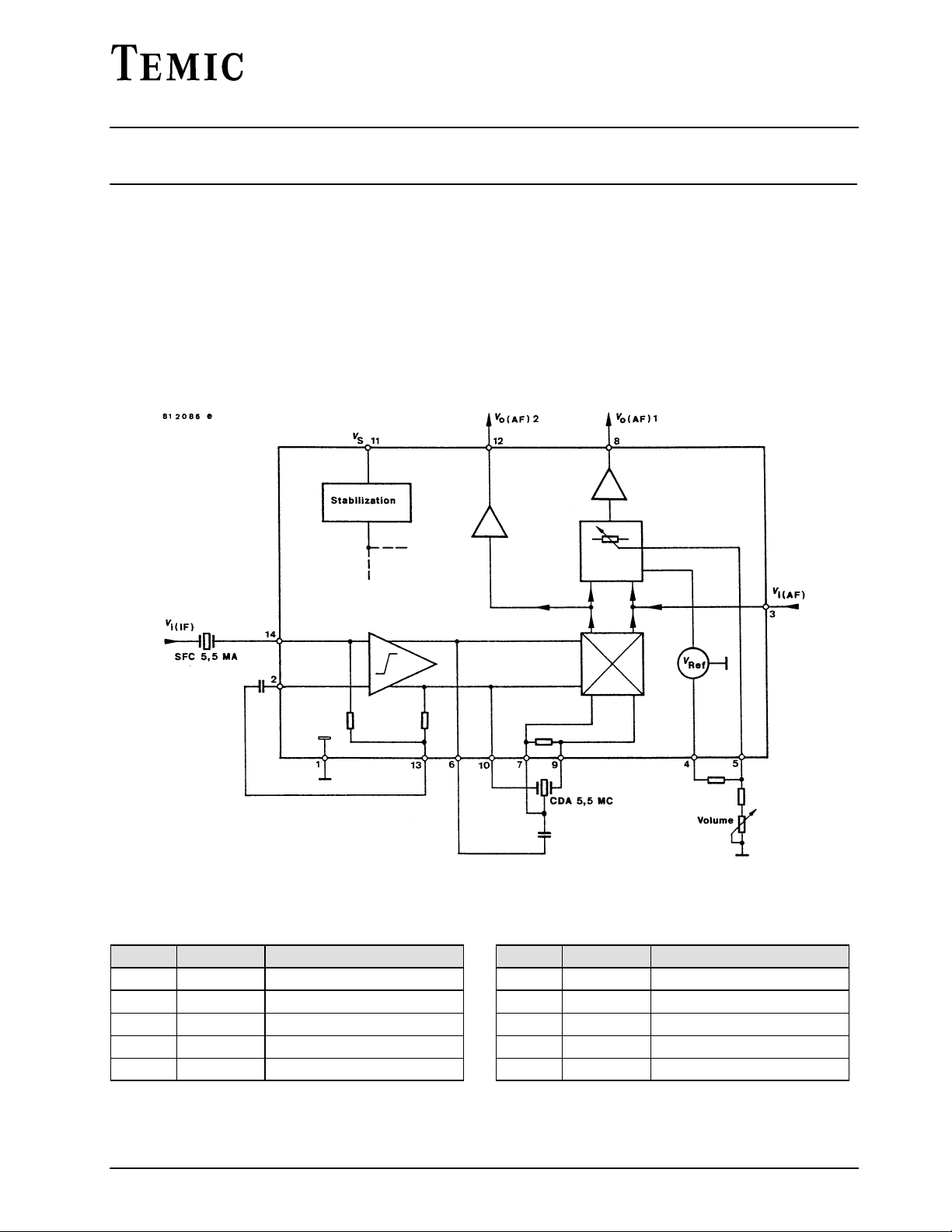
Pin Configuration
Pin Symbol Function
1 GND Ground
2, 13 Feedback
3 V
4 V
5 V
Rev . A1: 20.12.1994
i(AF)
ref
5
AF input – SCART
Reference voltage
Volume control
Figure 1 Block diagram
Pin Symbol Function
6,7,9,10 FM demodulator filter
8 V
11 V
12 V
14 V
o(AF)1
S
o(AF)2
i(IF)
AF output – controlled
Supply voltage
AF output – uncontrolled
IF input
1
TBA120T
TELEFUNKEN Semiconductors
Absolute Maximum Ratings
Reference point pin 1, unless otherwise specified
Parameters Symbol Value Unit
Supply voltage Pin 11 V
Volume setting voltage Pin 5 V
Reference supply current Pin 4 I
Power dissipation T
= 60°C P
amb
Ambient temperature range T
Storage temperature range T
S
5
Ref
tot
amb
stg
18 V
6 V
5 mA
400 mW
–15 to +70 °C
–25 to +125 °C
Electrical Characteristics
T
= +25°C, VS = 12 V, f = 5.5 MHz, Figure 3, reference point pin 1, unless otherwise specified
amb
Parameters Test Conditions / Pins Symbol Min. Typ. Max. Unit
Supply voltage range Pin 11 V
Supply current Pin 11 I
Reference voltage Pin 4 V
Output resistance Pin 4 r
S
S
oRef
Ref
Frequency range f 0 to 12 MHz
IF voltage gain Pin 6/14 G
Limited IF output voltage Pin 6 – 10 V
IF
o(IF)pp
Input limiting voltage f = 50 kHz,
f
= 1 kHz Pin 14 V
mod
Input impedance Pin 14 R
AM rejection m = 30 %, f = 50 kHz,
V
= 500 V, f
i
mod
= 1 kHz
DC voltage at AF output Vi = 0 Pin 8
Pin 12
Ripple rejection Pin 11/8
Pin 11/12
k
V
o(AF)1
V
o(AF)2
k
k
i(IF)
C
AM
Br
Br
i
i
IF residual voltage without de-emphasis
AF output voltage V
capacitor Pin 8
Pin 12
= 10 mV,
i
V
o(IF)1
V
o(IF)2
f =50 kHz,
f
= 1 kHz, R
mod
Output resistance Pin 8, 12 r
AF voltage amplification R
AF damping R
= 20 k, Pin 8/3 G
5
= 13 k, Fig. 3 Pin 8 –G
5
Volume setting range Pin 8 V
Input resistance Pin 3 r
= 20 k
5
Pin 8
Pin 12
V
o(AF)1
V
o(AF)2
o
v1
v1
o(AF)1
i
Mute function
Switching current
Pin 2 or 13
Switching voltage Figure 2 V
I
sw
mute
10 18 V
9.5 17.5 mA
4.2 4.8 5.5 V
12
68 dB
250 mV
30 60 V
800
5
pF
50 60 dB
4
5.6
35
V
V
dB
30
20
mV
30
650
400
900
650
mV
mV
1.1 k
7.5 dB
24 30 34 dB
70 85 dB
2 k
400 A
3 V
2
Rev . A1: 20.12.1994
 Loading...