

TEMIC U4224B-CFLG3, U4224B-CFL, T4224B-CC, T4224B-CF Datasheet
U4224B
Time Code Receiver
Description
The U4224B is a bipolar integrated straight through receiver circuit in the frequency range of 40 to 80 kHz.
The device is designed for radio controlled clock applications.
Features
D
D
Very low power consumption
D
Very high sensitivity
D
High selectivity by using two crystal filters
D
Power down mode available
Only a few external components necessary
D
Digitalized serial output signal
D
AGC hold mode
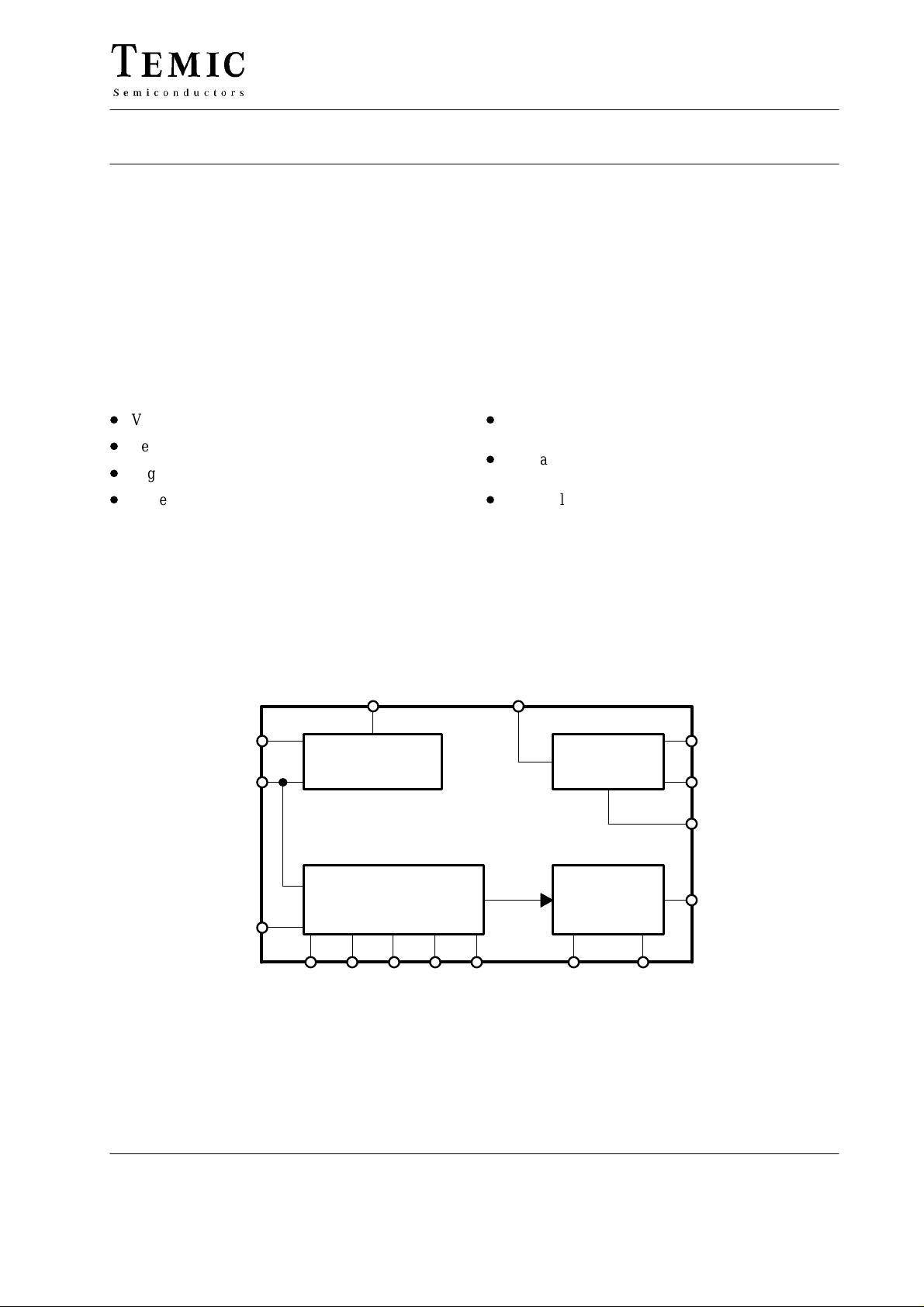
Block Diagram
GND
V
CC
IN
PON
3
1
2
Power Supply
4561314 7 8
SB
Q1A Q1B Q2A Q2B REC INT
15
AGC
Amplifier
TCO
16
Decoder
Rectifier &
Integrator
93 7727 e
11
10
12
FLB
FLA
9
DEC
SL
TELEFUNKEN Semiconductors
Rev . A3, 02-Apr-96
1 (17)
U4224B
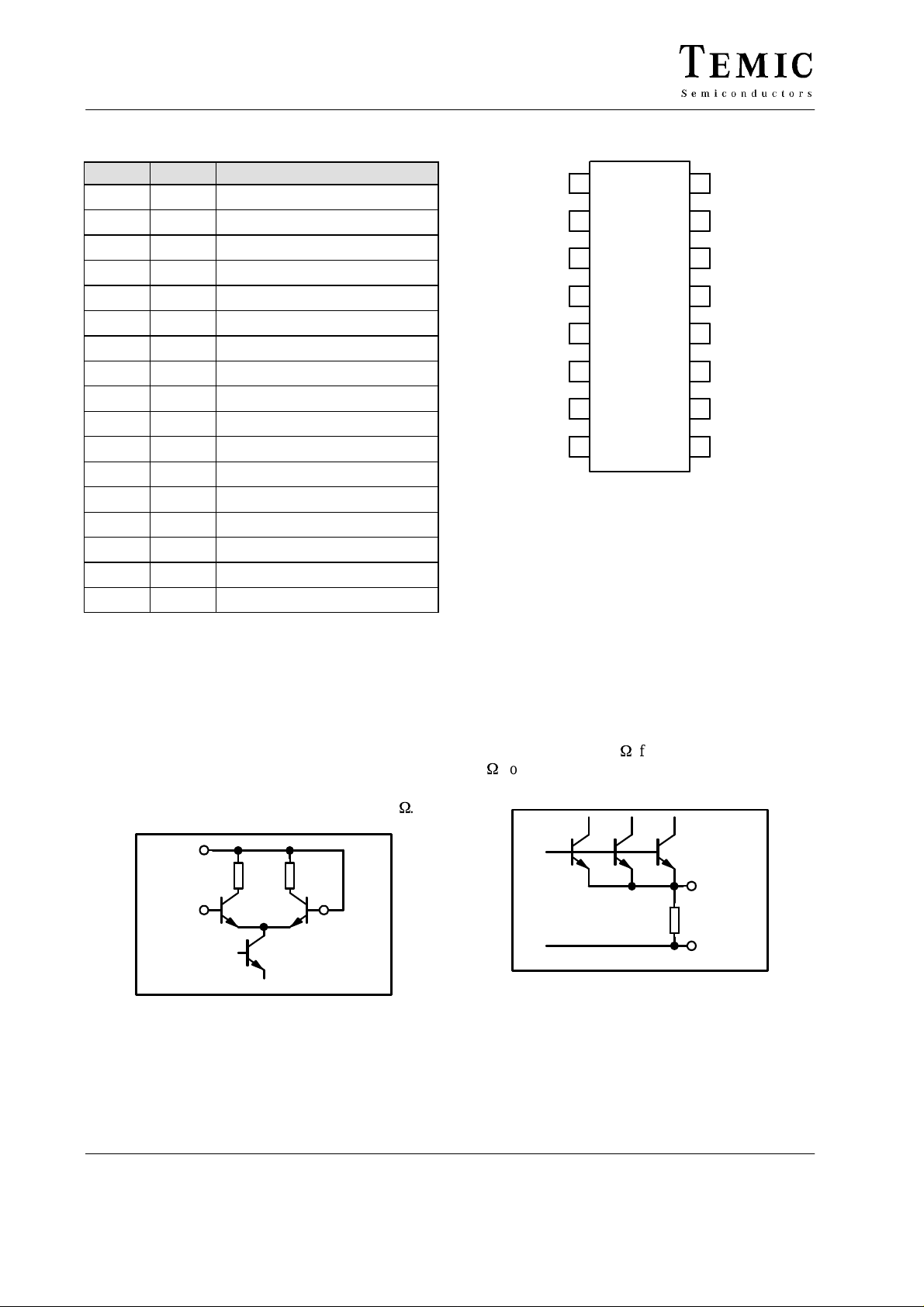
Pin Description
Pin Symbol Function
SO 16 L
1 V
2 IN Amplifier – Input
3 GND Ground
4 SB Bandwidth control
5 Q1A Crystal filter 1
6 Q1B Crystal filter 1
7 REC Rectifier output
8 INT Integrator output
9 DEC Decoder input
10 FLA Low pass filter
11 FLB Low pass filter
12 SL AGC hold mode
13 Q2A Crystal filter 2
14 Q2B Crystal filter 2
15 PON Power ON/OFF control
16 TCO Time code output
CC
Supply voltage
V
CC
IN
GND
SB
Q1A
Q1B
REC
INT
1
2
3
4
5
6
7
8
U4224B
93 7729 e
16
15
14
13
12
11
10
TCO
PON
Q2B
Q2A
SL
FLB
FLA
9
DEC
IN
A ferrite antenna is connected between IN and VCC. For
high sensitivity the Q of the antenna circuit should be as
high as possible, but a high Q often requires temperature
compensation of the resonant frequency. Specifications
are valid for Q > 30. An optimal signal to noise ratio will
be achieved by a resonant resistance of 50 to 200 kW.
V
CC
IN
94 8379
SB
A resistor RSB is connected between SB and GND. It controls the bandwidth of the crystal filters. It is
recommended: R
10 kW for 60 kHz WWVB and R
40 kHz.
= 0 W for DCF 77.5 kHz, RSB =
SB
= open for JG2AS
SB
94 8381
SB
GND
2 (17)
TELEFUNKEN Semiconductors
Rev . A3, 02-Apr-96
U4224B
Q1A, Q1B
In order to achieve a high selectivity, a crystal is connected between the pins Q1A
serial resonance frequency of the time code transmitter
(e.g. 60 kHz WWVB, 77.5 kHz DCF or 40kHz JG2AS).
The equivalent parallel capacitor of the filter crystal is
internally compensated. The compensated value is about
0.7 pF . If the full sensitivity and selectivity is not needed,
the crystal filter can be substituted by a capacitor of 10 pF
for DCF and WWVB and 22 pF for JG2AS.
Q1A
94 8382
and Q1B. It is used with the
Q1B
GND
REC
Rectifier output and integrator input: The capacitor C1
between REC and INT is the lowpass filter of the rectifier
and at the same time a damping element of the gain
control.
94 8374
SL
AGC hold mode: SL high (VSL = VCC) sets normal function, SL low (V
the voltage V
amplifier gain.
94 8378
= 0) disconnects the rectifier and holds
SL
at the integrator output and also the AGC
INT
V
CC
SL
INT
Integrator output: The voltage V
for the AGC. The capacitor C2 between INT and DEC
defines the time constant of the integrator. The current
through the capacitor is the input signal of the decoder.
is the control voltage
INT
94 8375
REC
GND
DEC
Decoder input: Senses the current through the integration
capacitor C2. The dynamic input resistance has a value of
about 420kW and is low compared to the impedance of
C2.
DEC
94 8376
GND
INT
GND
FLA, FLB
Lowpass filter: A capacitor C3 connected between FLA
and FLB supresses higher frequencies at the trigger
circuit of the decoder.
FLB
FLB
94 8377
TELEFUNKEN Semiconductors
Rev . A3, 02-Apr-96
3 (17)
U4224B
Q2A, Q2B
According to Q1A, Q1B a crystal is connected between
the pins Q2A and Q2B. It is used with the serial resonance
frequency of the time code transmitter (e.g. 60 kHz
WWVB, 77.5 kHz DCF or 40 kHz JG2AS). The equivalent parallel capacitor of the filter crystal is internally
compensated. The value of the compensation is about
0.7 pF.
Q2A Q2B
94 8383
GND
PON
If PON is connected to GND, the U 4224 B receiver IC
will be activated. The set-up time is typical 0.5s after
applying GND at this pin. If PON is connected to V
CC
, the
receiver will go into power down mode.
V
CC
PON
94 8373
TCO
The digitized serial signal of the time code transmitter can
be directly decoded by a microcomputer. Details about
the time code format of several transmitters are described
separately .
The output consists of a PNP*NPN push-pull-stage. It
should be taken into account that in the power down mode
(PON = high) TCO will be high.
V
CC
An additional improvement of the driving capability may
be achieved by using a CMOS driver circuit or a NPN
transistor with pull-up resistor connected to the collector
(see figure KEIN MERKER). Using a CMOS driver this
circuit must be connected to V
100 k
W
CC
.
10 k
V
CC
W
TCO
pin16
TCO
94 8395 e
Figure 1.
Please note:
The signals and voltages at the pins REC, INT , FLA, FLB,
Q1A, Q1B, Q2A and Q2B cannot be measured by standard measurement equipment due to very high internal
impedances. For the same reason the PCB should be protected against surface humidity.
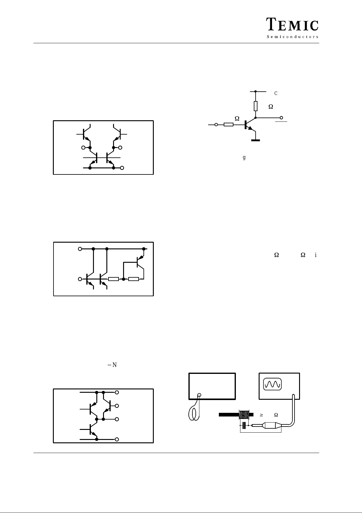
Design Hints for the Ferrite Antenna
The bar antenna is a very critical device of the complete
clock receiver. But by observing some basic RF design
knowledge, no problem should arise with this part. The IC
requires a resonance resistance of 50 kW to 200 kW. This
can be achieved by a variation of the L/C-relation in the
antenna circuit. But it is not easy to measure such high
resistances in the RF region. It is much more convenient
to distinguish the bandwidth of the antenna circuit and
afterwards to calculate the resonance resistance.
Thus the first step in designing the antenna circuit is to
measure the bandwidth. Figure 4 shows an example for
the test circuit. The RF signal is coupled into the bar
antenna by inductive means, e.g. a wire loop. It can be
measured by a simple oscilloscope using the 10:1 probe.
The input capacitance of the probe, typically about 10 pF ,
should be taken into consideration. By varying the
frequency of the signal generator, the resonance
frequency can be determined.
RF - Signal
generator
77.5 kHz
Scope
4 (17)
94 8380
PON
TCO
GND
wire loop
Probe
10 : 1
w
10 M
W
C
res
94 7907 e
TELEFUNKEN Semiconductors
Rev . A3, 02-Apr-96
U4224B
Afterwards, the two frequencies where the voltage of the
rf signal at the probe drops 3 dB down can be measured.
The difference between these two frequencies is called
the bandwidth BW
of the capacitor C
of the antenna circuit. As the value
A
in the antenna circuit is well known,
res
it is easy to compute the resonance resistance according
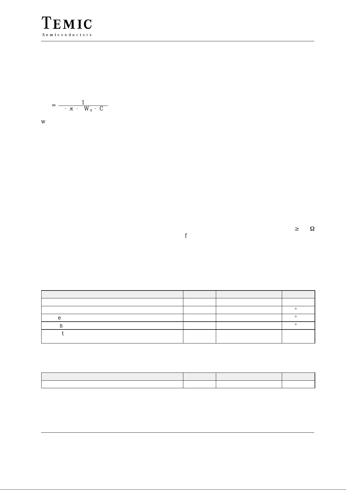
to the following formula:
+
R
res
2@p@BW
1
@
C
res
A
whereas
is the resonance resistance,
R
res
is the measured bandwidth (in Hz)
BW
A
is the value of the capacitor in the antenna circuit
C
res
(in Farad)
If high inductance values and low capacitor values are
used, the additional parasitic capacitances of the coil
must be considered. It may reach up to about 20 pF. The
Q-value of the capacitor should be no problem if a high
Q-type is used. The Q-value of the coil is more or less
distinguished by the simple DC-resistance of the wire.
Skin effects can be observed but do not dominate.
Therefore it shouldn’t be a problem to achieve the recommended values of resonance resistance. The use of thicker
wire increases Q and accordingly reduces bandwidth.
This is advantageous in order to improve reception in
noisy areas. On the other hand, temperature compensation of the resonance frequency might become a
problem if the bandwidth of the antenna circuit is low
compared to the temperature variation of the resonance
frequency . Of course, Q can also be reduced by a parallel
resistor.
Temperature compensation of the resonance frequency is
a must if the clock is used at different temperatures.
Please ask your dealer of bar antenna material and of capacitors for specified values of temperature coefficient.
Furthermore some critical parasitics have to be considered. These are shortened loops (e.g. in the ground line of
the PCB board) close to the antenna and undesired loops
in the antenna circuit. Shortened loops decrease Q of the
circuit. They have the same effect like conducting plates
close to the antenna. To avoid undesired loops in the
antenna circuit it is recommended to mount the capacitor
as close as possible to the antenna coil or to use a
C
res
twisted wire for the antenna coil connection. This twisted
line is also necessary to reduce feedback of noise from the
microprocessor to the IC input. Long connection lines
must be shielded.
A final adjustment of the time code receiver can be done
by pushing the coil along the bar antenna. The maximum
of the integrator output voltage V
at pin INT indicates
INT
the resonant point. But attention: The load current should
not exceed 1 nA, that means an input resistance w 1 G
W
of the measuring device is required. Therefore a special
DVM or an isolation amplifier is necessary .
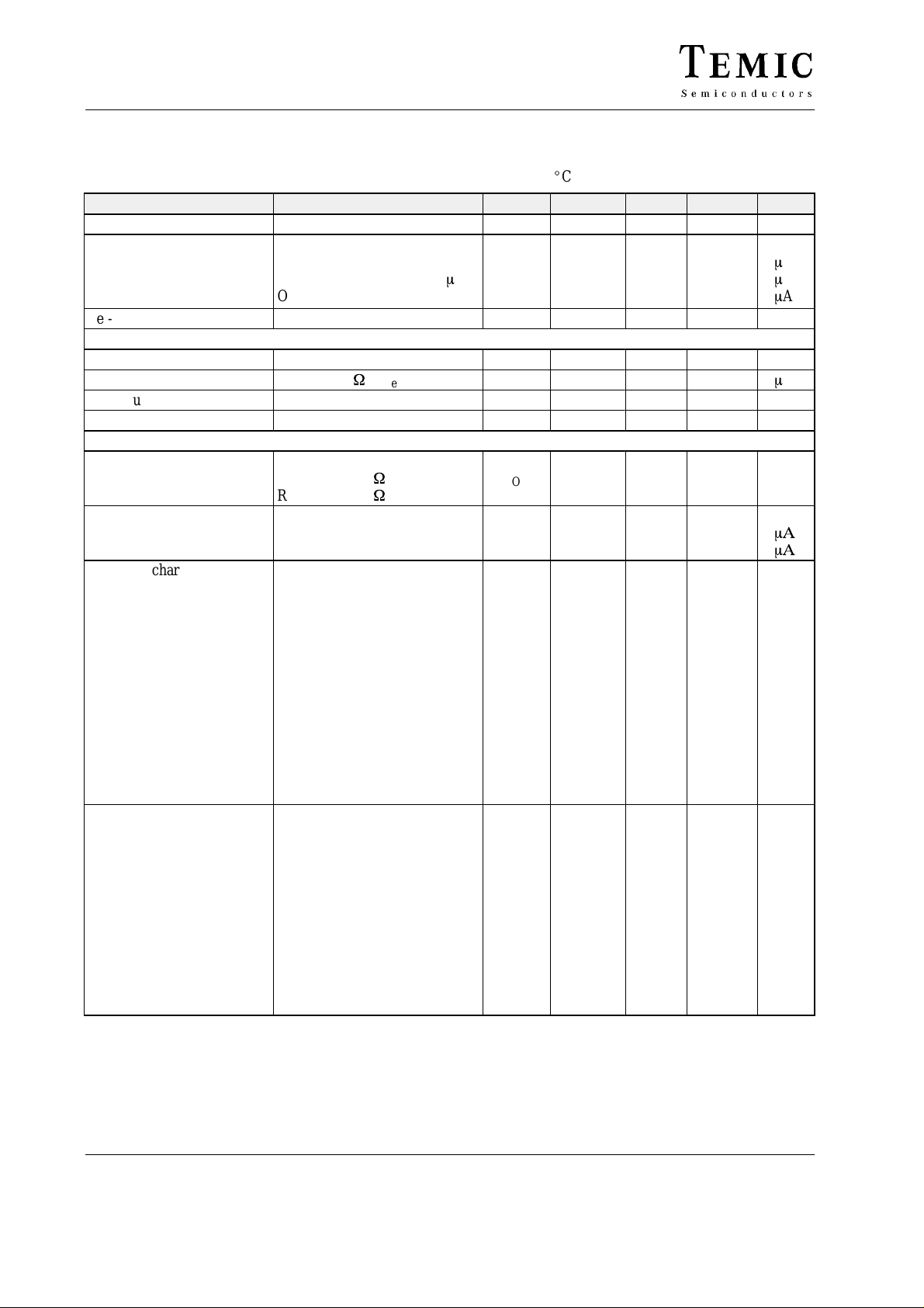
Absolute Maximum Ratings
Parameters Symbol Value Unit
Supply voltage V
Ambient temperature range T
Storage temperature range R
Junction temperature T
Electrostatic handling
± V
(MIL Standard 883 D), excepted pins 5, 6, 13 and 14
Thermal Resistance
Parameters Symbol Value Unit
Thermal resistance R
TELEFUNKEN Semiconductors
Rev . A3, 02-Apr-96
CC
amb
stg
j
ESD
thJA
5.25 V
–25 to +75
–40 to +85
125
2000 V
70 K/W
_
C
_
C
_
C
5 (17)
U4224B
Electrical Characteristics
VCC = 3 V, reference point pin 3, input signal frequency 80 kHz, T
= 25 _C, unless otherwise specified
amb
Parameters Test Conditions / Pin Symbol Min. Typ. Max. Unit
Supply voltage range pin 1 V
Supply current pin 1
without reception signal
with reception signal = 200mV
OFF-mode
CC
I
CC
1.2 5.25 V
30
15
25
0.1
Set-up time after VCC ON VCC = 1.5 V t 2 s
AGC AMPLIFIER INPUT; IN pin 2
Reception frequency range f
Minimum input voltage R
= 100 kW, Q
res
> 30 V
res
Maximum input voltage V
Input capacitance to ground C
in
in
in
in
40 80 kHz
1 1.5
40 80 mV
1.5 pF
TIMING CODE OUTPUT; TCO pin 16
Output voltage
HIGH
LOW
R
= 870 kW to GND
LOAD
R
= 650 kW to V
LOAD
CC
V
OH
V
OL
VCC-0.4
0.4
Output current
HIGH
LOW
V
V
TCO
TCO
= VCC/2
= VCC/2
I
SOURCE
I
SINK
3
4
10
12
Decoding characteristics DCF77 based on the values of
the application circuit
page KEIN MERKER:
TCO pulse width 100 ms
t
t
100
200
60
160
90
190
130
230
TCO pulse width 200 ms
m
A
m
A
m
A
m
V
V
V
mA
mA
ms
ms
Delay compared with the
transient of the RF signal:
drop down (start transition)
rise for 100 ms pulse
(end transition)
rise for 200 ms pulse
(end transition)
Decoding characteristics WWVB based on the values of
the application circuit
page KEIN MERKER:
TCO pulse width 200 ms
TCO pulse width 500 ms
TCO pulse width 800 ms
Delay compared with the
transient of the RF signal:
drop down (start transition)
rise (end transition)
t
t
t
200
t
500
t
800
t
s
e1
e2
30
25
10
140
440
740
t
s
t
e
45
20
60
55
30
200
500
800
80
45
ms
ms
ms
ms
ms
ms
ms
ms
6 (17)
TELEFUNKEN Semiconductors
Rev . A3, 02-Apr-96
 Loading...