

TEMIC M44C260, M48C260 Technical data
查询M44C260供应商
M44C260/M48C260
MARC4 – 4-bit Microcontroller
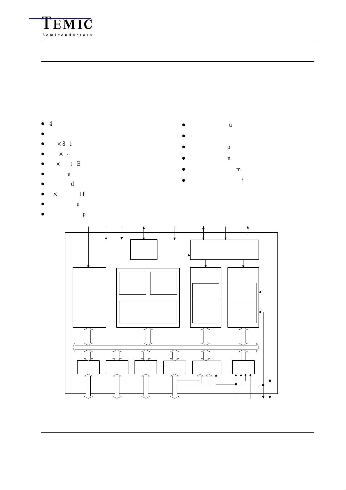
The M44C260 and M48C260 are members of the TEMIC family of 4-bit single chip microcontrollers. The M48C260
is the user programmable version of the M44C260. It contains an EEPROM program memory instead of a ROM. Both
microcontroller types contain RAM, EEPROM data memory , parallel I/O ports, one timer with watchdog function, two
8/16-bit multifunction timer/counter and the on-chip clock generation.
Features
D
4-bit HARVARD architecture
D
1 µs instruction cycle
D
4K 8-bit application program memory
D
256 4-bit RAM
D16
D
D
D2
D
D
8-bit EEPROM
16 bidirectional I/O’s
8 hard and software interrupt levels
8-bit multifunction timer/counter
Interval timer with watchdog
32 kHz on-chip oscillator
NWP
SS
V
V
EEPROM
16 x 8 bit
DD
NRST
Reset
ROM or
EEPROM
4K x 8 bit
MARC4
4–bit CPU core
Test
Sleep
RAM
256 x 4 bit
Benefits
D
Low power consumption
D
Power-down mode < 1 µA
D
2.4 to 6.2 V supply voltage
D
Self-test functions
D
High-level programming language in qFORTH
D
User programmable with the application program
TE TCL
Timer 1
Watch dog
Intervall
timer
OSCIN OSCOUT
Clock
Timer 2
Timer B
Timer A
I/O bus
IP40
Input
Port 4
IP43
TA
TB
94 9038
I/O
Port 0 Port 1 Port 2 Port 3
I/O I/O I/O
Figure 1. Block diagram
Interrupt
inputs
INT6
Rev . A2, 01-Oct-98 1 (51)
M44C260/M48C260
Á
Á
Á
Á
Á
Á
Á
Á
Á
Á
BP02
BP03
NWP
TE
OSC OUT
OSC IN
VDD
NRST
BP20
BP21
BP22
BP23
BP10
BP11
1
2
3
4
5
M44C260
6
7
M48C260
8
9
10
11
12
13
14 15
BP01
28
BP00
27
BP33
26
BP32
25
BP31
24
23
BP30
VSS
22
TCL
21
20
IP40–INT6
IP41–TA
19
IP42–TB
18
IP43
17
BP13
16
BP12
94 9039
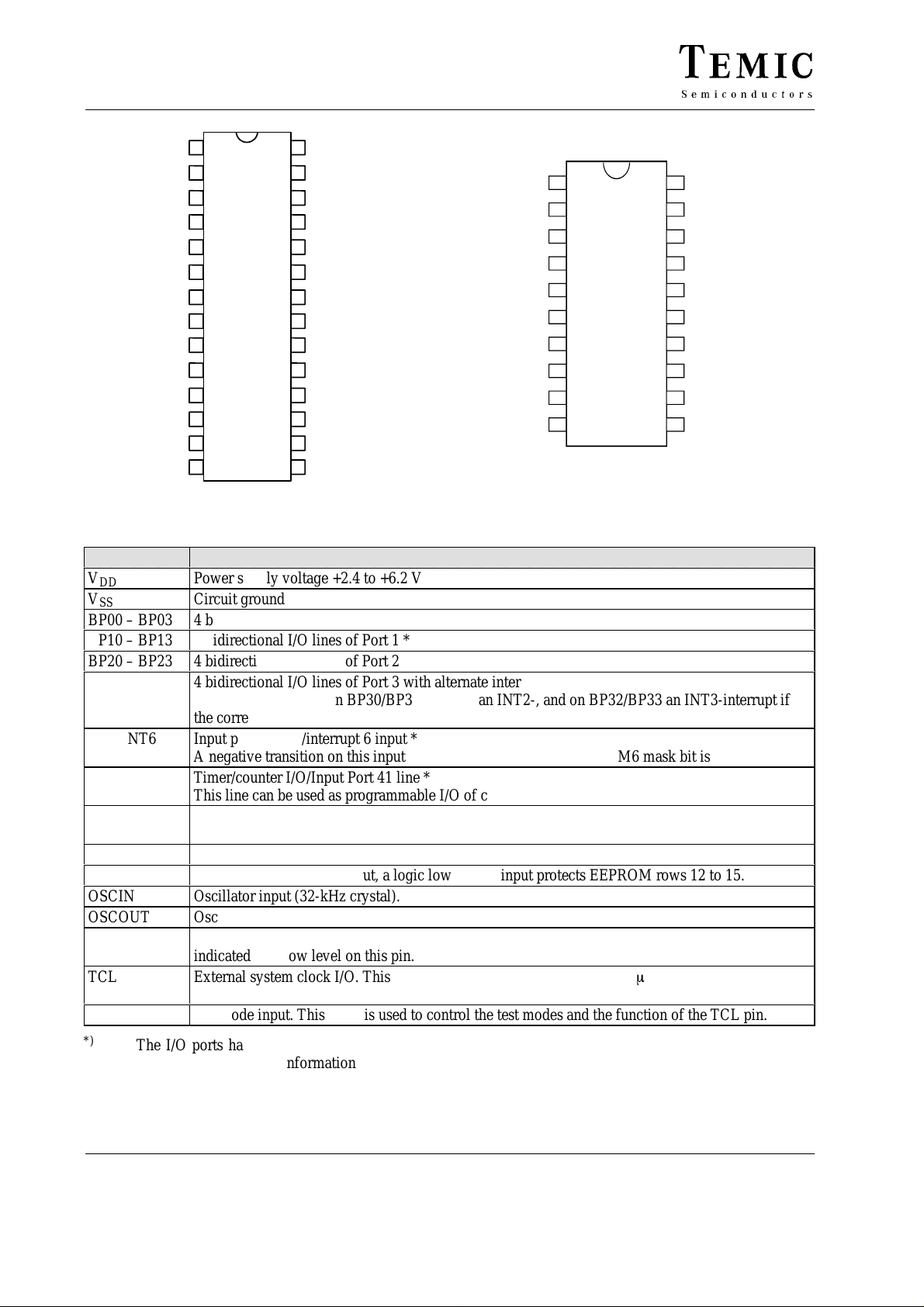
Figure 2. Pin connections for SSO28–FN
Table 1. Pin description
Name Function
V
DD
V
SS
BP00 – BP03
BP10 – BP13
BP20 – BP23
BP30 – BP33
ÁÁÁ
IP40-INT6
ÁÁÁ
IP41-TA
Power supply voltage +2.4 to +6.2 V
Circuit ground
4 bidirectional I/O lines of Port 0 *
4 bidirectional I/O lines of Port 1 *
4 bidirectional I/O lines of Port 2
4 bidirectional I/O lines of Port 3 with alternate interrupt function.
A negative transition on BP30/BP31 requests an INT2-, and on BP32/BP33 an INT3-interrupt if
ББББББББББББББББББББББББББ
the corresponding interrupt-mask is set.
Input port 40 line/interrupt 6 input *
A negative transition on this input requests an INT6 interrupt if the IM6 mask bit is set.
ББББББББББББББББББББББББББ
Timer/counter I/O/Input Port 41 line *
This line can be used as programmable I/O of counter A or as Port 41 input.
IP42-TB
ÁÁÁ
IP43
NWP
OSCIN
OSCOUT
NRST
ÁÁÁ
TCL
ÁÁÁ
TE
*)
The I/O ports have CMOS output buffers. As input they are available with pull-up or pull-down resistors.
Timer/counter I/O/input Port 42 line *
ББББББББББББББББББББББББББ
This line can be used as programmable I/O of counter B or as Port 42 input.
Input Port 43 line
*)
EEPROM write protect input, a logic low on this input protects EEPROM rows 12 to 15.
Oscillator input (32-kHz crystal).
Oscillator output (32-kHz crystal).
Reset input/output, a logic low on this pin resets the device. An internal watchdog reset is
ББББББББББББББББББББББББББ
indicated by a low level on this pin.
External system clock I/O. This pin can be used as input to provide the mC with an external
clock or as output of the internal system clock.
ББББББББББББББББББББББББББ
T estmode input. This input is used to control the test modes and the function of the TCL pin.
Please see the ordering information.
1
BP02
BP03
2
TE
3
VDD
NRST
BP20
BP10
BP11
4
5
M44C260
6
7
8
9
10
OSC OUT
OSC IN
Figure 3. Pin connections for SSO20
20
BP01
19
BP00
BP31
18
BP30
17
16
VSS
TCL
15
INT6
–IP40
14
–IP
TA
13
12
11
41
BP13
BP12
Rev . A2, 01-Oct-982 (51)

M44C260/M48C260
Contents
1 MARC4 Architecture 5. . . . . . . . . . . . . . . . . . . . . . . . . . . . . . . . . . . . . . . . . . . . . . . . . . . . . . . . . . . . . . .
1.1 General Description 5. . . . . . . . . . . . . . . . . . . . . . . . . . . . . . . . . . . . . . . . . . . . . . . . . . . . . . . . . .
1.2 Components of MARC4 Core 5. . . . . . . . . . . . . . . . . . . . . . . . . . . . . . . . . . . . . . . . . . . . . . . . . .
1.2.1 Program Memory (ROM or EEPROM) 5. . . . . . . . . . . . . . . . . . . . . . . . . . . . . . . . . .
1.2.2 Data Memory (RAM) 6. . . . . . . . . . . . . . . . . . . . . . . . . . . . . . . . . . . . . . . . . . . . . . . .
1.2.3 Registers 7. . . . . . . . . . . . . . . . . . . . . . . . . . . . . . . . . . . . . . . . . . . . . . . . . . . . . . . . . .
1.2.4 ALU 8. . . . . . . . . . . . . . . . . . . . . . . . . . . . . . . . . . . . . . . . . . . . . . . . . . . . . . . . . . . . .
1.2.5 Self-Check 8. . . . . . . . . . . . . . . . . . . . . . . . . . . . . . . . . . . . . . . . . . . . . . . . . . . . . . . .
1.2.6 Instruction Cycles 8. . . . . . . . . . . . . . . . . . . . . . . . . . . . . . . . . . . . . . . . . . . . . . . . . . .
1.2.7 I/O Bus 8. . . . . . . . . . . . . . . . . . . . . . . . . . . . . . . . . . . . . . . . . . . . . . . . . . . . . . . . . . .
1.2.8 Interrupt Structure 9. . . . . . . . . . . . . . . . . . . . . . . . . . . . . . . . . . . . . . . . . . . . . . . . . . .
Software Interrupts 10. . . . . . . . . . . . . . . . . . . . . . . . . . . . . . . . . . . . . . . . . . . . . . . . . .
Hardware Interrupts 10. . . . . . . . . . . . . . . . . . . . . . . . . . . . . . . . . . . . . . . . . . . . . . . . .
1.3 Reset 10. . . . . . . . . . . . . . . . . . . . . . . . . . . . . . . . . . . . . . . . . . . . . . . . . . . . . . . . . . . . . . . . . . . . . .
1.4 Clock Generation 11. . . . . . . . . . . . . . . . . . . . . . . . . . . . . . . . . . . . . . . . . . . . . . . . . . . . . . . . . . . .
1.4.1 Clock Status/Control Register (CSC) 12. . . . . . . . . . . . . . . . . . . . . . . . . . . . . . . . . . . .
1.4.2 TCL Signal 12. . . . . . . . . . . . . . . . . . . . . . . . . . . . . . . . . . . . . . . . . . . . . . . . . . . . . . . .
1.5 Power Down Modes 12. . . . . . . . . . . . . . . . . . . . . . . . . . . . . . . . . . . . . . . . . . . . . . . . . . . . . . . . . .
2 Peripheral Modules 13. . . . . . . . . . . . . . . . . . . . . . . . . . . . . . . . . . . . . . . . . . . . . . . . . . . . . . . . . . . . . . . .
2.1 Addressing Peripherals 13. . . . . . . . . . . . . . . . . . . . . . . . . . . . . . . . . . . . . . . . . . . . . . . . . . . . . . . .
2.1.1 Input Port 4 15. . . . . . . . . . . . . . . . . . . . . . . . . . . . . . . . . . . . . . . . . . . . . . . . . . . . . . . .
2.1.2 Bidirectional Ports 15. . . . . . . . . . . . . . . . . . . . . . . . . . . . . . . . . . . . . . . . . . . . . . . . . .
2.1.3 External Interrupt Inputs 16. . . . . . . . . . . . . . . . . . . . . . . . . . . . . . . . . . . . . . . . . . . . . .
2.2 Timer 1 17. . . . . . . . . . . . . . . . . . . . . . . . . . . . . . . . . . . . . . . . . . . . . . . . . . . . . . . . . . . . . . . . . . . .
2.2.1 T1C – Timer 1 Control Register 18. . . . . . . . . . . . . . . . . . . . . . . . . . . . . . . . . . . . . . . .
2.2.2 WDC – Watchdog Control Register 18. . . . . . . . . . . . . . . . . . . . . . . . . . . . . . . . . . . . .
2.3 Timer 2 19. . . . . . . . . . . . . . . . . . . . . . . . . . . . . . . . . . . . . . . . . . . . . . . . . . . . . . . . . . . . . . . . . . . .
2.3.1 Timer 2 Status/Control Register (T2SC) 21. . . . . . . . . . . . . . . . . . . . . . . . . . . . . . . . .
2.3.2 Timer 2 Subport (T2SUB) 22. . . . . . . . . . . . . . . . . . . . . . . . . . . . . . . . . . . . . . . . . . . .
2.3.3 Timer 2 Reload Register 22. . . . . . . . . . . . . . . . . . . . . . . . . . . . . . . . . . . . . . . . . . . . . .
2.3.4 Timer 2 Capture Register 23. . . . . . . . . . . . . . . . . . . . . . . . . . . . . . . . . . . . . . . . . . . . .
2.3.5 Timer A Mode Register 1 (TAM1) 23. . . . . . . . . . . . . . . . . . . . . . . . . . . . . . . . . . . . . .
2.3.6 Timer A Mode Register 2 (TAM2) 24. . . . . . . . . . . . . . . . . . . . . . . . . . . . . . . . . . . . . .
2.3.7 Timer B Mode Register 1 (TBM1) 24. . . . . . . . . . . . . . . . . . . . . . . . . . . . . . . . . . . . . .
2.3.8 Timer B Mode Register 2 (TBM2) 25. . . . . . . . . . . . . . . . . . . . . . . . . . . . . . . . . . . . . .
2.3.9 Timer 2 Prescaler Control Register (T2PC) 25. . . . . . . . . . . . . . . . . . . . . . . . . . . . . . .
2.3.10 Timer 2 Interrupt Control Register (T2IC) 26. . . . . . . . . . . . . . . . . . . . . . . . . . . . . . . .
2.3.11 Timer I/O (TA/TB) 27. . . . . . . . . . . . . . . . . . . . . . . . . . . . . . . . . . . . . . . . . . . . . . . . . .
2.4 EEPROM 28. . . . . . . . . . . . . . . . . . . . . . . . . . . . . . . . . . . . . . . . . . . . . . . . . . . . . . . . . . . . . . . . . .
2.4.1 EEPROM SubPort (ESUB) 28. . . . . . . . . . . . . . . . . . . . . . . . . . . . . . . . . . . . . . . . . . .
2.4.2 EEPROM Mode/Status Register (EMS) 29. . . . . . . . . . . . . . . . . . . . . . . . . . . . . . . . . .
Rev . A2, 01-Oct-98 3 (51)

M44C260/M48C260
Contents (continued)
3 Appendix 30. . . . . . . . . . . . . . . . . . . . . . . . . . . . . . . . . . . . . . . . . . . . . . . . . . . . . . . . . . . . . . . . . . . . . . . . .
3.1 Emulation 30. . . . . . . . . . . . . . . . . . . . . . . . . . . . . . . . . . . . . . . . . . . . . . . . . . . . . . . . . . . . . . . . . .
3.2 Programming the EEPROM Program Memory 30. . . . . . . . . . . . . . . . . . . . . . . . . . . . . . . . . . . . .
3.3 MARC4 Instruction Set 30. . . . . . . . . . . . . . . . . . . . . . . . . . . . . . . . . . . . . . . . . . . . . . . . . . . . . . .
3.3.1 MARC4 Instruction Set Overview 31. . . . . . . . . . . . . . . . . . . . . . . . . . . . . . . . . . . . . .
3.3.2 qFOR TH Language Overview 32. . . . . . . . . . . . . . . . . . . . . . . . . . . . . . . . . . . . . . . . .
3.4 The qFORTH Language - Quick Reference Guide 33. . . . . . . . . . . . . . . . . . . . . . . . . . . . . . . . . .
3.4.1 Arithmetic/Logical 33. . . . . . . . . . . . . . . . . . . . . . . . . . . . . . . . . . . . . . . . . . . . . . . . . .
3.4.2 Comparisons 33. . . . . . . . . . . . . . . . . . . . . . . . . . . . . . . . . . . . . . . . . . . . . . . . . . . . . . .
3.4.3 Control Structures 34. . . . . . . . . . . . . . . . . . . . . . . . . . . . . . . . . . . . . . . . . . . . . . . . . . .
3.4.4 Stack Operations 34. . . . . . . . . . . . . . . . . . . . . . . . . . . . . . . . . . . . . . . . . . . . . . . . . . . .
3.4.5 Memory Operations 35. . . . . . . . . . . . . . . . . . . . . . . . . . . . . . . . . . . . . . . . . . . . . . . . .
3.4.6 Predefined Structures 36. . . . . . . . . . . . . . . . . . . . . . . . . . . . . . . . . . . . . . . . . . . . . . . .
3.4.7 Assembler Mnemonics 36. . . . . . . . . . . . . . . . . . . . . . . . . . . . . . . . . . . . . . . . . . . . . . .
4 Electrical Characteristics 38. . . . . . . . . . . . . . . . . . . . . . . . . . . . . . . . . . . . . . . . . . . . . . . . . . . . . . . . . . . .
4.1 Absolute Maximum Ratings 38. . . . . . . . . . . . . . . . . . . . . . . . . . . . . . . . . . . . . . . . . . . . . . . . . . . .
4.2 DC Operating Characteristics 38. . . . . . . . . . . . . . . . . . . . . . . . . . . . . . . . . . . . . . . . . . . . . . . . . . .
4.3 AC Characteristics 39. . . . . . . . . . . . . . . . . . . . . . . . . . . . . . . . . . . . . . . . . . . . . . . . . . . . . . . . . . .
4.4 Schmitt-Trigger Inputs 45. . . . . . . . . . . . . . . . . . . . . . . . . . . . . . . . . . . . . . . . . . . . . . . . . . . . . . . .
5 Pad Layout 46. . . . . . . . . . . . . . . . . . . . . . . . . . . . . . . . . . . . . . . . . . . . . . . . . . . . . . . . . . . . . . . . . . . . . . .
6 Package Information 48. . . . . . . . . . . . . . . . . . . . . . . . . . . . . . . . . . . . . . . . . . . . . . . . . . . . . . . . . . . . . . .
7 Standard Design of M48C260 49. . . . . . . . . . . . . . . . . . . . . . . . . . . . . . . . . . . . . . . . . . . . . . . . . . . . . . . .
8 Ordering Information for M44C260 50. . . . . . . . . . . . . . . . . . . . . . . . . . . . . . . . . . . . . . . . . . . . . . . . . .
Rev . A2, 01-Oct-984 (51)
1 MARC4 Architecture
1.1 General Description
M44C260/M48C260
MARC4 CORE
Reset
Program
PC
memory
Reset
Clock
System
clock
Sleep
Instruction
bus
Instruction
decoder
Interrupt
controller
I/O bus
On–chip peripheral modules
Figure 4. MARC4 core
The MARC4 microcontroller consists of an advanced
stack based 4-bit CPU core and on-chip peripherals. The
CPU is based on the HARVARD architecture with a
physically separate program memory (ROM or
EEPROM) and data memory (RAM). Three independent
buses the instruction bus, the memory bus and the I/O bus
are used for parallel communication between program
memory, RAM and peripherals. This enhances program
execution speed by allowing both instruction prefetching,
and simultaneous communication to the on-chip peripheral circuitry. The integrated powerful interrupt
controller with eight prioritized interrupt levels, supports
fast processing of hardware events.
The MARC4 is designed for the high level programming
language qFORTH. The core contains both FORTH
stacks, expression stack and return stack. This architecture allows high level language programming without any
loss in efficiency or code density.
1.2 Components of MARC4 Core
The core contains a program memory, RAM, ALU, program counter, RAM address register, instruction decoder
X
Y
SP
RAM
256 x 4-bit
RP
Memory bus
TOS
CCR
and interrupt controller. The following sections describe
each of these parts.
1.2.1 Program Memory (ROM or
EEPROM)
The ROM is mask programmed with the application program during the fabrication of the microcontroller. The
EEPROM is programmed by the customer using a special
programming device (see chapter ”Progamming the
EEPROM Program Memory”). The program memory is
addressed by a 12-bit wide program counter, thus limiting
the program size to a maximum of 4 Kbytes. The
M44C260 contains an additional 1 Kbyte ROM for test
software. The program memory starts with a 512 byte segment (zero page) which contains predefined start
addresses for interrupt service routines and special subroutines accessible with single byte instructions
(SCALL). The corresponding memory map is shown in
the figure 4.Look-up tables of constants can also be held
in the program memory and are accessed via the
MARC4’s built-in TABLE instruction.
ALU
94 8973
Rev . A2, 01-Oct-98 5 (51)
M44C260/M48C260
FFFh
Program
memory
(4K x 8-bit)
Self test
bank (1K)
only
1FFh
M44C260
Zero page
000h
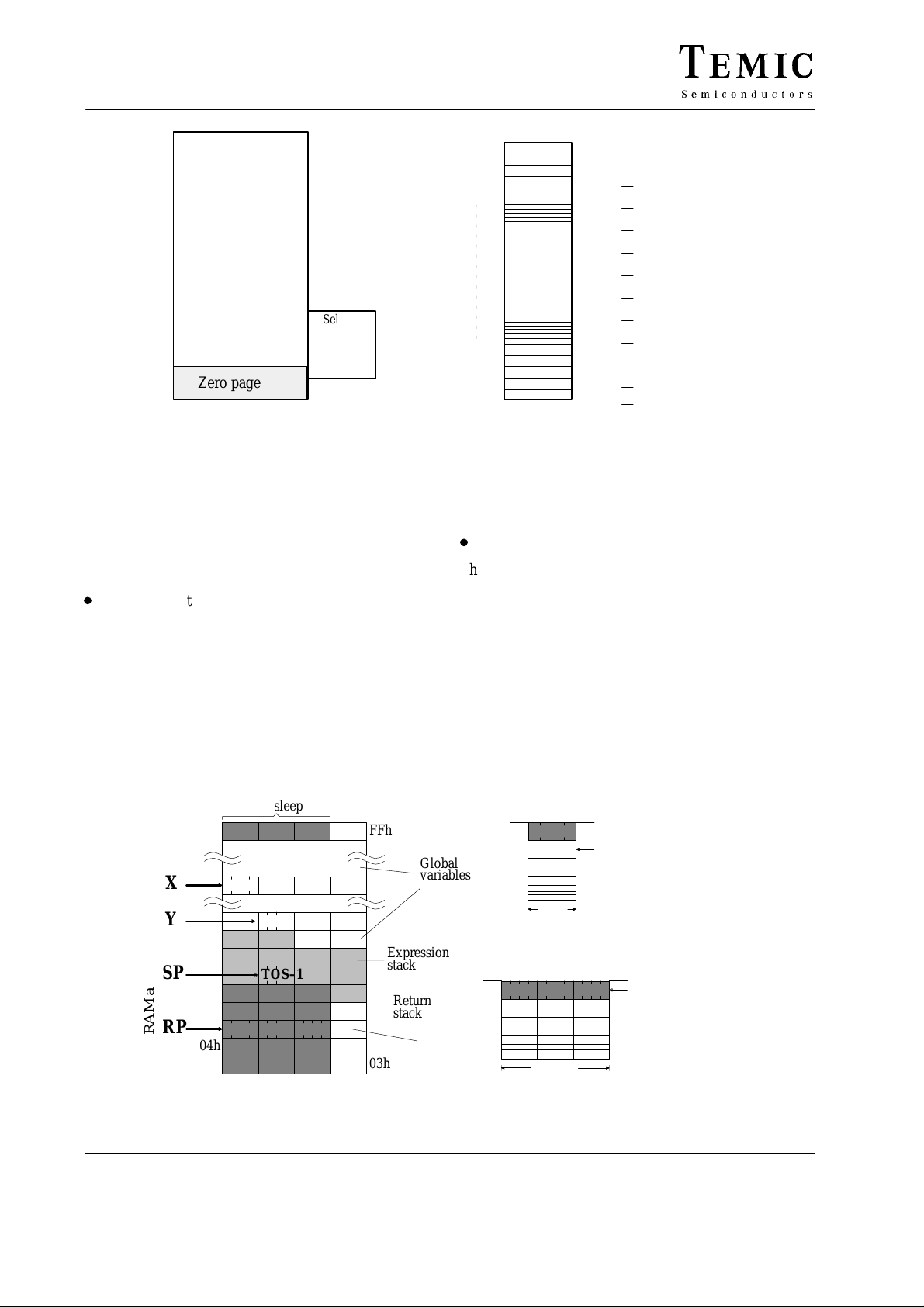
1.2.2 Data Memory (RAM)
The MARC4 contains a 256 x 4-bit wide static random access memory (RAM). It is used for the expression stack,
the return stack and data memory for variables and arrays.
The RAM is addressed by any of the four 8-bit wide RAM
address registers SP, RP, X and Y.
D
Expression Stack
The 4-bit wide expression stack is addressed with the expression stack pointer (SP). All arithmetic, I/O and
memory reference operations take their operands from,
and return their result to the expression stack. The
MARC4 performs the operations with the top of stack
items (TOS and TOS-1). The TOS register contains the
3FFh
000h
Figure 5. Program memory map
1F8h
1F0h
1E8h
1E0h
SCALL addresses
020h
018h
010h
008h
000h
Zero
page
1E0h
1C0h
180h
140h
100h
0C0h
080h
040h
008h
000h
INT7
INT6
INT5
INT4
INT3
INT2
INT1
INT0
$RESET
$AUTOSLEEP
94 8974
top element of the expression stack and works like an
accumulator. This stack is also used for passing parameters between subroutines, and as a scratchpad area for
temporary storage of data.
D
Return Stack
The 12-bit wide return stack is addressed by the return
stack pointer (RP). It is used for storing return addresses
of subroutines, interrupt routines and for keeping loop index counts. The return stack can also be used as a
temporary storage area.
The MARC4 instruction set supports the exchange of data
between the top elements of the expression stack and the
return stack. The two stacks within the RAM have a user
definable location and maximum depth.
RAM
(256 x 4-bit)
Autosleep
FCh
X
Y
SP
RP
RAM address register:
04h
00h
TOS–1
FFh
Global
variables
Expression
stack
Return
stack
Global
07h
03h
v
variables
Figure 6. RAM map
Expression stack
30
TOS
TOS–1
TOS–2
4-bit
SP
Return stack
11
12-bit
0
RP
94 8975
Rev . A2, 01-Oct-986 (51)
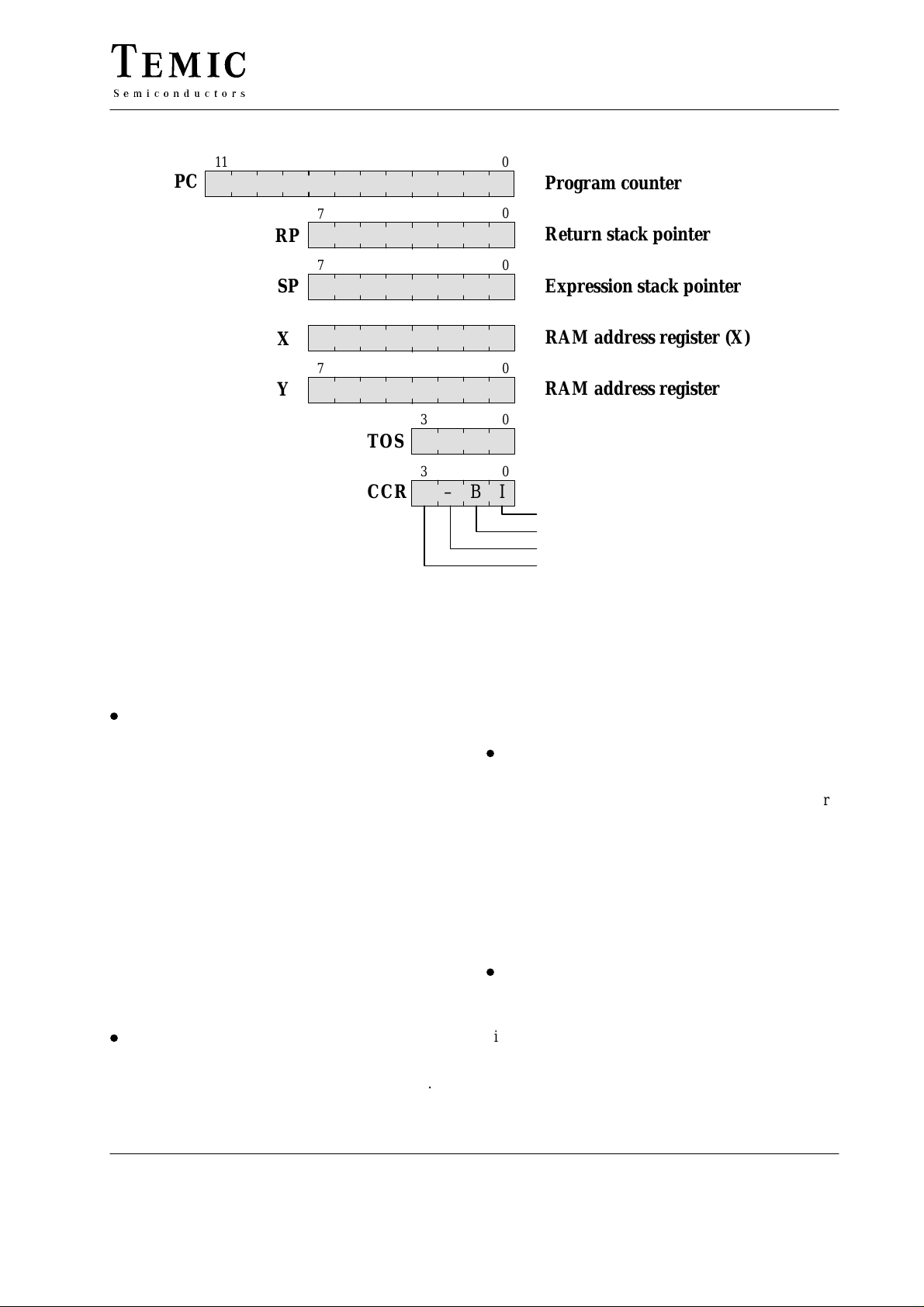
1.2.3 Registers
11
PC
M44C260/M48C260
0
Program counter
7
RP
7
SP
7
X
Y
3
TOS
3
CCR
The MARC4 controller has six programmable registers
and one condition code register. They are shown in
figure 7.
D
Program Counter (PC)
The program counter (PC) is a 12-bit register that contains
the address of the next instruction to be fetched from the
program memory. Instructions currently being executed
are decoded in the instruction decoder to determine the
internal micro operations. For linear code (no calls or
branches) the program counter is incremented with every
instruction cycle. If a branch-, call-, return-instruction or
an interrupt is executed the program counter is loaded
with a new address. The program counter is also used with
the TABLE instruction to fetch 8-bit wide ROM
constants.
RAM Address Register
The RAM is addressed with the four 8-bit wide RAM
address registers: SP, RP, X and Y. These registers allow
access to any of the 256 RAM nibbles.
D
Expression Stack Pointer (SP)
The stack pointer (SP) contains the address of the next-totop 4-bit item (TOS-1) of the expression stack. The
pointer is automatically pre-incremented if a nibble is
moved onto the stack, or post-decremented if a nibble is
C
–
Figure 7. Programming model
0
00
Return stack pointer
0
Expression stack pointer
0
RAM address register (X)
07
RAM address register (Y)
0
Top of stack register
0
B
I
Condition code register
Interrupt enable
Branch
Unused
Carry / borrow
removed from the stack. Every post-decrement operation
moves the item (TOS-1) to the TOS register before the SP
is decremented. After a reset, the stack pointer has to be
initialized with ” >SP $xx ” to allocate the start address
of the expression stack area.
D
Return Stack Pointer (RP)
The return stack pointer points to the top element of the
12-bit wide return stack. The pointer automatically preincrements if an element is moved onto the stack or it
post-decrements if an element is removed from the stack.
The return stack pointer increments and decrements in
steps of 4. This means that every time a 12-bit element is
stacked, a 4-bit RAM location is left unwritten. This location is used by the qFORTH compiler to allocate 4-bit
variables. After a reset the return stack pointer has to be
initialized with ” >RP FCh ”.
D
RAM Address Register (X and Y)
The X and Y registers are used to address any 4-bit item
in the RAM. A fetch operation moves the addressed
nibble onto the TOS. A store operation moves the TOS to
the addressed RAM location. By using either the pre-increment or post-decrement addressing mode arrays in the
RAM can be compared, filled or moved.
94 8976
Rev . A2, 01-Oct-98 7 (51)
M44C260/M48C260
D
T op Of Stack (TOS)
The top of stack register is the accumulator of the
MARC4. All arithmetic/logic, memory reference and I/O
operations use this register . The TOS register gets the data
from the ALU, the program memory, the RAM or via the
I/O bus.
D
Condition Code Register (CCR)
The 4-bit wide condition code register contains the
branch, the carry and the interrupt enable flag. These bits
indicate the current state of the CPU. The CCR flags are
set or reset by ALU operations. The instructions
SET_BCF, TOG_BF, CCR! and DI allow a direct
manipulation of the condition code register .
Carry/Borrow (C)
The carry/borrow flag indicates that borrow or carry out
of arithmetic logic unit (ALU) occurred during the last
arithmetic operation. During shift and rotate operations
this bit is used as a fifth bit. Boolean operations have no
affect on the C flag.
Branch (B)
The branch flag controls the conditional program branching. When the branch flag has been set by one of the
previous instructions a conditional branch is taken. This
flag is affected by arithmetic, logic, shift, and rotate operations.
Interrupt Enable (I)
The interrupt enable flag enables or disables the interrupt
processing on a global basis. After reset or by executing
the DI instruction, the interrupt enable flag is reset and all
interrupts are disabled. The µC does not process further
interrupt requests until the interrupt enable flag is set
again by either executing an EI, RTI or SLEEP
instruction.
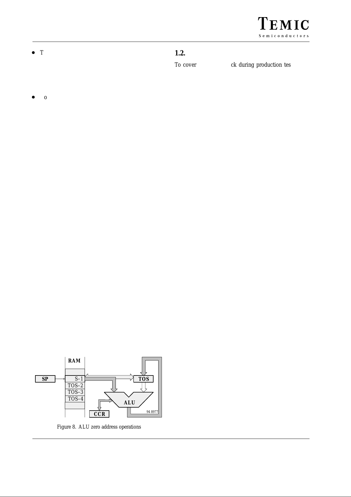
1.2.4 ALU
The 4-bit ALU performs all the arithmetic, logical, shift
and rotate operations with the top two elements of the
expression stack (TOS and TOS-1) and returns its result
to the TOS. The ALU operations affect the carry/borrow
and branch flag in the condition code register (CCR).
RAM
SP
TOS–1
TOS–2
TOS–3
TOS–4
CCR
Figure 8. ALU zero address operations
ALU
TOS
94 8977
1.2.5 Self-Check
To cover the ROM block during production testing the
ROM_TEST2 routine has to be included into the $RESET
routine.
: $RESET >SP S0
>RP FCh
Port7 IN Fh =
IF ROM_Test2
THEN
\*** main program
;
Note: The corresponding file ROM_TEST.INC has to
be included into the project’s main file. The
conditional execution is stimulated during the
production test.
1.2.6 Instruction Cycles
A MARC4 instruction word is one or two bytes long and
is executed within one or four machine-cycles. A
machine-cycle consists of two system clocks (SYSCL).
The MARC4 is a zero address machine. Most of the
instructions are one byte long and are executed only in
one machine-cycle. The CPU has an instruction pipeline,
which allows the controller to fetch the next instruction
from program memory at the same time as the present
instruction is being executed. For more information see
the section ”MARC4 Instruction Set Overview”.
1.2.7 I/O Bus
The I/O ports and the registers of the peripheral modules
(Timer 1, Timer 2, EEPROM) are I/O mapped. The communication between the core and the on-chip peripherals
takes place via the I/O bus and the associated I/O control
bus. These buses are used for different functions: for read
and write accesses, for the interrupt generation, to reset
peripherals and for the SLEEP mode. With the MARC4
IN-instruction and OUT-instruction the I/O bus allows a
direct read or write access to one of the 16 I/O addresses.
More about the I/O access to the on-chip peripherals is
described in the section ”Peripheral modules”.
The I/O buses are internal buses and are not accessible by
the customer on the final microcontroller device, but they
are used as the interface for the MARC4 emulation (see
also the section “Emulation”).
Rev . A2, 01-Oct-988 (51)
M44C260/M48C260
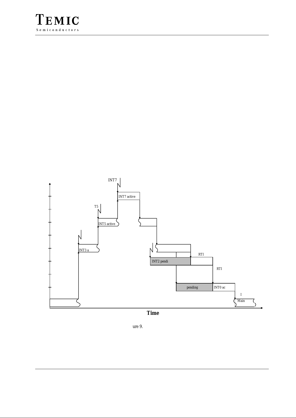
1.2.8 Interrupt Structure
The MARC4 can handle interrupts with eight different
priority levels. They can be generated from the internal
and external interrupt sources or by a software interrupt
from the CPU itself. Each interrupt level has a hard-wired
priority and an associated vector for the service routine in
the ROM (see table 2). The programmer can enable or disable interrupts all together by setting or resetting the
interrupt enable flag (I) in the CCR.
Interrupt Processing
For processing the eight interrupt levels, the MARC4
contains an interrupt controller with the 8-bit wide interrupt pending and interrupt active register. The interrupt
controller samples all interrupt requests during every
non-I/O instruction cycle and latches them in the interrupt
pending register. If no higher priority interrupt is present
in the interrupt active register it signals the CPU to interrupt the current program execution. If the interrupt enable
bit is set the processor enters an interrupt acknowledge
cycle. During this cycle a SHORT CALL instruction to
INT7
the service routine is executed and the current PC is saved
on the return stack. An interrupt service routine is finished
with the RTI instruction. This instruction sets the interrupt
enable flag, resets the corresponding bits in the interrupt
pending/active register and fetches the return address
from the return stack to the program counter. When the
interrupt enable flag is reset (interrupts are disabled), the
execution of interrupts is inhibited but not the logging of
the interrupt requests in the interrupt pending register.
The execution of the interrupt will be delayed until the
interrupt enable flag is set again. But note that interrupts
are lost if an interrupt request occurs during the corresponding bit in the pending register is still set. After the
reset (power-on, external or watchdog reset), the interrupt
enable flag and the interrupt pending and interrupt active
register are reset.
Interrupt Latency
The interrupt latency is the time from the falling edge of
the interrupt to the interrupt service routine being
activated. In the MARC4 this takes between 3 to 5
machine cycles depending on the state of the core.
7
6
5
4
3
Priority level
2
1
0
Main /
Autosleep
INT3
INT5
INT3 active
INT5 active
INT7 active
RTI
INT2
INT2 pending
Time
Figure 9. Interrupt handling
RTI
SWI0
INT2 active
INT0 pending
RTI
RTI
INT0 active
RTI
Main /
Autosleep
94 8978
Rev . A2, 01-Oct-98 9 (51)
M44C260/M48C260
Á
Á
Á
Á
Á
Á
Á
Á
Á
Á
Á
Á
Á
Á
Á
Á
Á
Á
Á
Á
Á
Á
Á
Á
Á
Á
Á
Table 2. Interrupt priority table
Interrupt Priority Vector
Address
INT0
INT1
INT2
ÁÁÁ
INT3
ÁÁÁ
INT4
INT5
INT6
ÁÁÁ
INT7
lowest
040h
080h
0C0h
ÁÁÁÁÁÁ
100h
ÁÁÁÁÁÁ
140h
180h
1C0h
ÁÁÁÁÁÁ
highest
1E0h
Interrupt Opcode
(Acknowledge)
C8h (SCALL 040h)
D0h (SCALL 080h)
D8h (SCALL 0C0h)
ББББББ
E0h (SCALL 100h)
ББББББ
E8h (SCALL 140h)
F0h (SCALL 180h)
F8h (SCALL 1C0h)
ББББББ
FCh (SCALL 1E0h)
Function
Software interrupt (SWI0)
EEPROM write ready
External hardware interrupt,
ББББББББББББ
neg. edge at BP30 or BP31
External hardware interrupt,
neg. edge at BP32 or BP33
ББББББББББББ
Timer 1 interrupt
Timer 2 interrupt
External hardware interrupt, neg. edge at
ББББББББББББ
IP40 pin
Software interrupt (SWI7)
Software Interrupts
The programmer can generate interrupts by using the
software interrupt instruction (SWI) which is supported
in qFORTH by predefined macros named SWI0 to SWI7.
The software triggered interrupt operates exactly as any
hardware triggered interrupt. The SWI instruction takes
the top two elements from the expression stack and writes
the corresponding bits via the I/O bus to the interrupt
Table 3. Hardware interrupts
Interrupt Priority Mask Interrupt Source
Register Bit
EEPROM write ready
External interrupt
Port 3 (BP30 OR BP31)
External interrupt
ББББББББ
Port 3 (BP32 OR BP33)
Timer 1 interrupt
Timer 2 interrupt
ББББББББ
ББББББББ
Ext. interrupt IP40 input
INT1
INT2
INT3
ÁÁ
INT4
INT5
ÁÁ
ÁÁ
INT6
EMS
IMR1
IMR1
ÁÁ
IMR2
T2IC
ÁÁ
ÁÁ
IMR2
pending register. By using the SWI instruction in thius
way , interrupts can be re-prioritized or lower priority processes scheduled for later execution.
Hardware Interrupts
The M44C260/M48C260 incorporates eleven hardware
interrupt sources with six different levels. Each of these
sources can be enabled or disabled separately with an interrupt mask bit in the IMR1 or IMR2 register.
IMEP
IM30
IM31
IM32
ÁÁ
IM33
IMT1
IMAS
IMAP
ÁÁ
IMBS
ÁÁ
IMBP
IM6
EEPROM end of write cycle
Negative edge at BP30
Negative edge at BP31
Negative edge at BP32
ББББББББББББ
Negative edge at BP33
Timer 1
Timer A end of space/underflow
Timer A end of pulse/capture
ББББББББББББ
Timer B end of space/underflow
ББББББББББББ
Timer B end of pulse/capture
Negative edge at IP40 input
1.3 Reset
The reset puts the CPU into a well-defined condition. The
reset can be triggered by switching on the supply voltage,
by a break-down of the supply voltage, by the watchdog
timer or by pulling the NRST pad to low.
After any reset the branch-, carry- and interrupt enable
flag in the Condition Code Register (CCR) , the interrupt
pending register and the interrupt active register are reset.
During the reset-cycle the I/O bus control signals are set
to ’reset mode’ thereby initializing all on-chip
peripherals.
A reset is finished with a short call instruction
(opcode C1h) to the program memory address 008h. This
activates the initialization routine $RESET. With that
routine the stack pointers, variables in the RAM and the
peripheral must be initialized.
Rev . A2, 01-Oct-9810 (51)
M44C260/M48C260
Power-on Reset
The M44C260/M48C260 incorporates an on-chip
power-on reset (POR) circuitry which provides internal
chip reset for most power-up situations. The power-on
reset ensures that the core is not activated before the operating supply voltage has been reached.
The mC will function normally at > 2.4 V under all conditions. For V
below 2.4 V, the device will either
DD
function normally or the device reset will be globally activated by the brown-out circuit. The actual brown-out trip
point is a function of temperature and process parameters.
External Reset (NRST)
An external reset can be triggered with the NRST pin. For
the external reset the pin should be low for a minimum of
two machine-cycles.
Watchdog Timer Reset
If the watchdog timer function of Timer 1 is enabled, a reset is triggered with every watchdog counter overflow. To
suppress that, the watchdog counter must be reset by an
access to the CWD-register (see also Timer 1/watchdog
counter).
The power-on reset and the watchdog reset are indicated
in the same way as an external reset on the NRST pad.
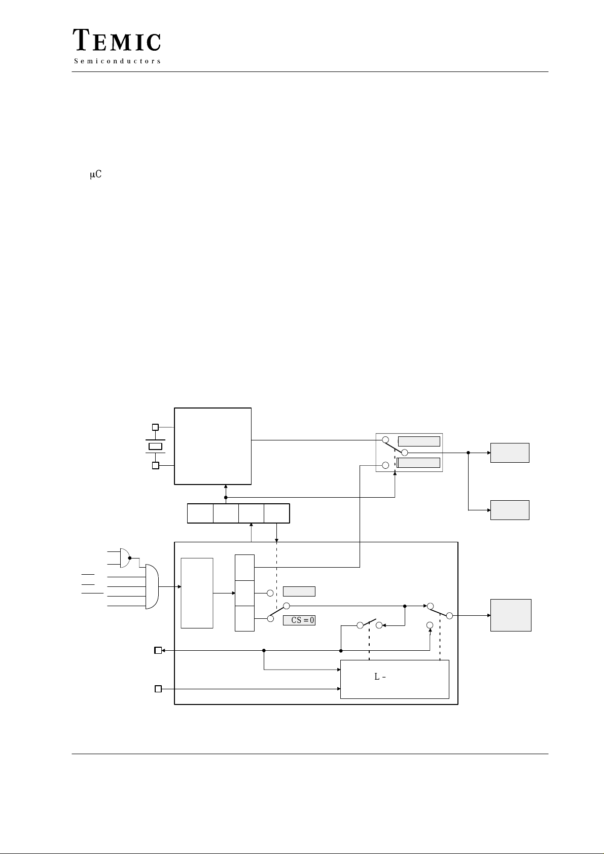
1.4 Clock Generation
The M44C260/M48C260 has two oscillators, one RC oscillator for the system clock generation and an additional
32-kHz crystal oscillator. The system clock generator
provides the core and Timer 2 with the clock. The system
clock frequency is programmable for 1 or 2 MHz. The
crystal oscillator is used as an exact time base for Timer
1. If no exact timing is required, the controller does not
need an external crystal. In this case Timer 1 is provided
with the system clock.
The configuration for both oscillators is programmable
with the clock status control register (CSC), which is a
subport register located in port CSUB. The required configuration has to be initialized after reset in the $RESET
routine. The default setting after a reset is 1 MHz system
clock and an active 32-kHz crystal oscillator.
After power-on or a SLEEP instruction the clock generator needs a start-up time until it runs with an exact timing.
The CRDY bit in the CSC register indicates the start-up
phase.
OSCS
T1R
TAR
TBR
EERDY
SLEEP
OSCIN
Q1
OSCOUT
TCL
TE
CSC :
CSC3
OSC
Stop
OSC32
Stop
OSCS CRDY CCS
/122
/2
/4
f
OSC
= 32 kHz
CCS = 1
CCS = 0
OSCS = 0
OSCS = 1
<= 32 kHz
f
G
Systemclock –
Generator
TCL – Controllogic
CL32
SYSCL
TIMER 1
EEPROM
TIMER 2
CORE
94 8979
Figure 10. Clock module
Rev . A2, 01-Oct-98 11 (51)
M44C260/M48C260
Á
Á
Á
Á
Á
Á
Á
Á
Á
Á
Á
Á
Á
Á
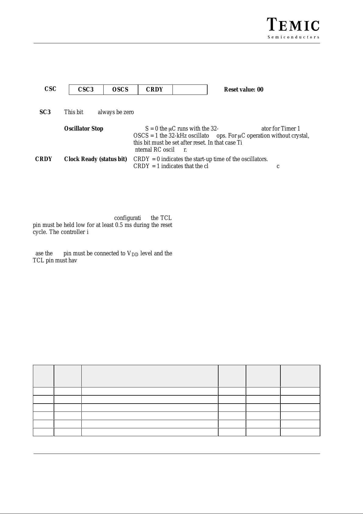
1.4.1 Clock Status/Control Register (CSC)
Bit 3 Bit 2 Bit 1 Bit 0
CSC
ÁÁÁ
CSC3
ÁÁÁ
OSCS
ÁÁ
CRDY
ÁÁÁ
CCS
ÁÁÁ
Address: Ch Subaddress: 2h
Reset value: 0000h
БББББББ
CSC3
ÁÁ
OSCS
ÁÁ
ÁÁ
CRDY
ÁÁ
CCS
This bit must always be zero
БББББББББББББББББББББББББББ
Oscillator Stop OSCS = 0 the mC runs with the 32-kHz crystal oscillator for Timer 1
БББББББББББББББББББББББББББ
БББББББББББББББББББББББББББ
OSCS = 1 the 32-kHz oscillator stops. For mC operation without crystal,
this bit must be set after reset. In that case Timer 1 is provided from the
internal RC oscillator.
Clock Ready (status bit) CRDY = 0 indicates the start-up time of the oscillators.
БББББББББББББББББББББББББББ
CRDY = 1 indicates that the clock is ready and has the exact timing.
Core Clock Select CCS = 0 selects 1 MHz system clock (SYSCL/TCL)
CCS = 1 selects 2 MHz system clock (SYSCL/TCL)
1.4.2 TCL Signal
The TCL pin can be used as input to supply the controller
with an external clock. For this configuration, the TCL
pin must be held low for at least 0.5 ms during the reset
cycle. The controller is working with clock frequencies
up to 2.5 MHz. It is also possible to use the TCL pin as
output to supply peripherals with the system clock. In this
case the TE pin must be connected to V
level and the
DD
TCL pin must have a high impedance load.
1.5 Power Down Modes
The sleep mode is a shutdown condition which is used to
reduce the average system power consumption in applications where the µC is not fully utilized. In this mode the
system clock is stopped. The sleep mode is entered with
the SLEEP instruction. This instruction sets the interrupt
enable bit (I) in the condition code register to enable all
interrupts and stops the core. During the sleep mode the
peripheral modules remain active and are able to generate
interrupts. The µC exits the sleep mode with any interrupt
or a reset.
Table 4. Power consumption at different power down modes
Mode CPU-
Core
1
SLEEP
2
SLEEP
3
SLEEP
4
SLEEP
5
6
RUN
RUN
T1R=0 AND TAR=0 AND TBR=0 AND EERDY=1
T1R=X, TAR=0 AND TBR=0 AND EERDY=1
T1R=1 OR TAR=1 OR TBR=1 OR EERDY=0
T1R=X, TAR=1 OR TBR=1 OR EERDY=0
T1R=X, T AR=X, TBR=X, EERDY=X
T1R=X, T AR=X, TBR=X, EERDY=X
TIMER 1 [T1R]
TIMER 2 [TAR, TBR]
EEPROM [EERDY]
The sleep mode can only be kept when none of the interrupt pending or active register bits are set. The application
of the $AUTOSLEEP routine ensures the correct function
of the sleep mode.
The total power consumption is directly proportional to
the active time of the µC. For a rough estimation of the
expected average system current consumption, the following formula should be used:
(VDD, f
I
total
I
depends on VDD and f
DD
Osc
) = I
+ (IDD * T
Sleep
Osc
.
active/Ttotal
)
Systemclock Generator Stop
The M44C260/M48C260 has different power down
modes. When the MARC4 core enters the sleep mode and
no on-chip peripheral needs a clock signal (SYSCL), the
system clock oscillator is stopped. Therefore the programmer should stop Timer 1 and Timer 2 during the
sleep mode if they are not required. If the 32-kHz oscillator is not used, it should be stopped. Under this condition,
the power consumption is extremely low (see following
table).
RC Osc. 32-kHz-
Osc.
Power-
Consumption
[OSCS]
STOP
STOP
RUN
RUN
RUN
RUN
STOP
RUN
STOP
RUN
STOP
RUN
< 1.0 µA
< 1.0 µA
< 1 mA
< 1 mA
< 3 mA
< 3 mA
Rev . A2, 01-Oct-9812 (51)
2 Peripheral Modules
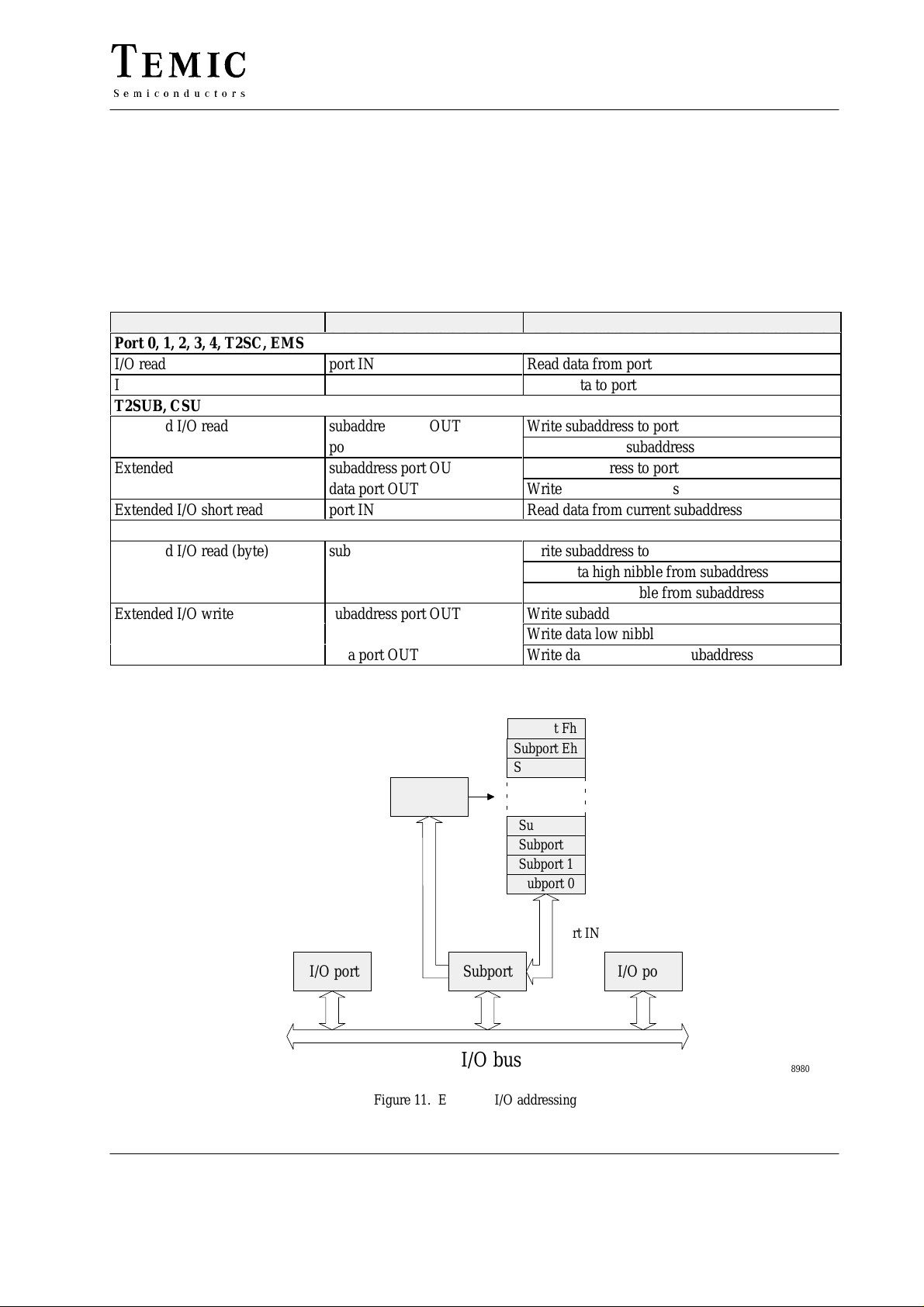
2.1 Addressing Peripherals
The access to the peripheral modules (ports, registers) is
executed via the I/O bus. The IN- or OUT-instruction allows the direct addressing of 16 I/O ports. For peripherals
with a large number of registers, extended addressing is
used. With two I/O operations, an extended I/O port al-
Table 5. I/O-addressing
I/O Operation qFOR TH Instructions Description
Port 0, 1, 2, 3, 4, T2SC, EMS
I/O read
I/O write
T2SUB, CSUB
Extended I/O read
Extended I/O write
Extended I/O short read
ESUB
Extended I/O read (byte)
Extended I/O write (byte)
port IN
data port OUT
subaddress port OUT
port IN
subaddress port OUT
data port OUT
port IN
subaddress port OUT
port IN
port IN
subaddress port OUT
data port OUT
data port OUT
M44C260/M48C260
lows the access to 16 subports. The first OUT-instruction
writes the subport address to the subaddress register, the
second IN- or OUT-instruction reads data from or writes
data to the addressed subport.
Read data from port
Write data to port
Write subaddress to port
Read data from subaddress
Write subaddress to port
Write data to subaddress
Read data from current subaddress
Write subaddress to port
Read data high nibble from subaddress
Read data low nibble from subaddress
Write subaddress to port
Write data low nibble to subaddress
Write data high nibble to subaddress
Subport Fh
Subport Eh
Subport Dh
Subaddress
Register
Subport 3
Subport 2
subaddress port OUT
I/O port Subport I/O port
I/O bus
Figure 11. Extended I/O addressing
Rev . A2, 01-Oct-98 13 (51)
Subport 1
Subport 0
data port OUT
port IN
94 8980
M44C260/M48C260
Á
Á
Á
Á
Á
Á
Á
Á
Á
Á
Á
Á
Á
Á
Á
Á
Á
Á
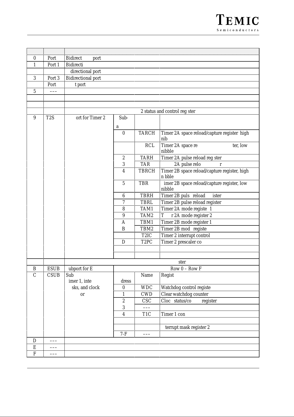
Table 6. Peripheral addresses
Addr. Name Function
0
Port 0
1
Port 1
2
Port 2
3
Port 3
4
Port 4
5
6
7
8
9
–––
–––
–––
T2SC
T2SUB
Bidirectional port
Bidirectional port
Bidirectional port
Bidirectional port
Input port
Subport for Timer 2
Timer 2 status and control register
Sub-
Name
Register
Á
ÁÁ
БББББ
address
ÁÁ
0
1
ÁÁÁÁÁБББББÁÁÁ
2
3
4
5
ÁÁÁÁÁБББББÁÁÁ
6
7
8
9
A
B
C
D
E
F
A
B
C
Á
EMS
ESUB
CSUB
ÁÁ
Subport for EEPROM
Subport for watchdog,
БББББ
Timer 1, interrupt
masks, and clock
generator
Sub-
ÁÁ
address
0
1
2
3
4
5
6
7-F
D
E
F
–––
–––
–––
ÁÁÁ
TARCH
ББББББББББББ
Timer 2A space reload/capture register , high
nibble
TARCL
ÁÁÁ
TARH
TARL
TBRCH
Timer 2A space reload/capture register , low
ББББББББББББ
nibble
Timer 2A pulse reload register
Timer 2A pulse reload register
Timer 2B space reload/capture register , high
nibble
TBRCL
ÁÁÁ
TBRH
TBRL
TAM1
TAM2
TBM1
TBM2
T2IC
T2PC
Timer 2B space reload/capture register , low
ББББББББББББ
nibble
Timer 2B pulse reload register
Timer 2B pulse reload register
Timer 2A mode register 1
Timer 2A mode register 2
Timer 2B mode register 1
Timer 2B mode register 2
Timer 2 interrupt control
Timer 2 prescaler control
–––
–––
EEPROM status register
Row 0 – Row F
Name
ÁÁÁ
WDC
CWD
CSC
Register
ББББББББББББ
Watchdog control register
Clear watchdog counter
Clock status/control register
–––
T1C
IMR1
IMR2
Timer 1 control register
Interrupt mask register 1
Interrupt mask register 2
–––
Rev . A2, 01-Oct-9814 (51)
M44C260/M48C260
2.1.1 Input Port 4
Port 4 is the input port for the pins IP40, IP43, TA and TB. IP40 is also the interrupt input for INT6, and TA and TB
are normally used for timer I/O functions.
Bit 3 Bit 2 Bit 1 Bit 0
Input Port 4
IP43
TB/IP42
TA/IP41
IP40/INT6
V
DD
*
Pull–up
I/O bus
V
DD
IP43
*
Pull–down
Figure 12. Input port IP40, IP43
2.1.2 Bidirectional Ports
Ports 0, 1, 2 and 3 are bidirectional 4-bit wide ports and
may be used for data input or output. The data direction
is programmable for a complete port only. The port is
switched to output with an OUT-instruction and to input
with an IN-instruction. The data written to a port will be
stored into the output latches and appears immediately
after the OUT -instruction at the port pin. After RESET all
output latches are set to Fh and the ports are switched to
input mode.
Note: Care must be taken when switching bidirectional
ports from output to input. The capacitive load at
this port may cause the data read to be the same
as the last data written to this port. To avoid this
when switching the direction, one of the following approaches should be used.
V
DD
*
Pull–up
I/O bus
IP40/INT6
INT6
* optional
D
Use two IN-instructions and DROP the first data
nibble read. The first IN switches the port from output
to input, DROP removes the first invalid nibble and
the second IN reads the valid nibble.
D
Use an OUT-instruction followed by an IN-instruction. With the OUT-instruction, the capacitive load is
charged or discharged depending on the optional
pull-up /pull-down configuration. Write a “1” for pins
with pull-up resistors and a “0” for pins with pulldown resistors.
94 8981
Rev . A2, 01-Oct-98 15 (51)
M44C260/M48C260
I/O bus
D
R
Reset
OUT
IN
/ Reset
SQQ
R
NQ
Figure 13. Bidirectional port
V
DD
V
DD
*) optional
pull–up / pull–down
resistor
*
BPxy
*
94 8982
Interrupt logic
I/O bus
PortX_OUT
PortX_IN
/ Reset
(INT2 / INT3)
D
R
Reset
SQQ
*) optional
R
NQ
Figure 14. Bidirectional Port 3 with interrupt input
pull–up / pull–down
resistor
V
DD
*
V
DD
BP3y
*
94 8983
2.1.3 External Interrupt Inputs
The pins IP40 and BP30 – BP33 can be used as external
interrupt inputs. IP40 is used for INT6, BP32 and BP33
are used for INT3, and BP30 and BP31 are used for INT2.
Pin IP40 is also used as an input port and BP30 – BP33 as
a bidirectional port (see figure 14). Each of these external
interrupt sources can be enabled or disabled with individual interrupt mask bits. A negative transition at one of
these inputs requests an interrupt, when the corresponding mask bit is set. The interrupt masks are placed in the
subport registers IMR1 and IMR2 of port CSUB.
Rev . A2, 01-Oct-9816 (51)
 Loading...