

查询M44C260供应商
M44C260/M48C260
MARC4 – 4-bit Microcontroller
The M44C260 and M48C260 are members of the TEMIC family of 4-bit single chip microcontrollers. The M48C260
is the user programmable version of the M44C260. It contains an EEPROM program memory instead of a ROM. Both
microcontroller types contain RAM, EEPROM data memory , parallel I/O ports, one timer with watchdog function, two
8/16-bit multifunction timer/counter and the on-chip clock generation.
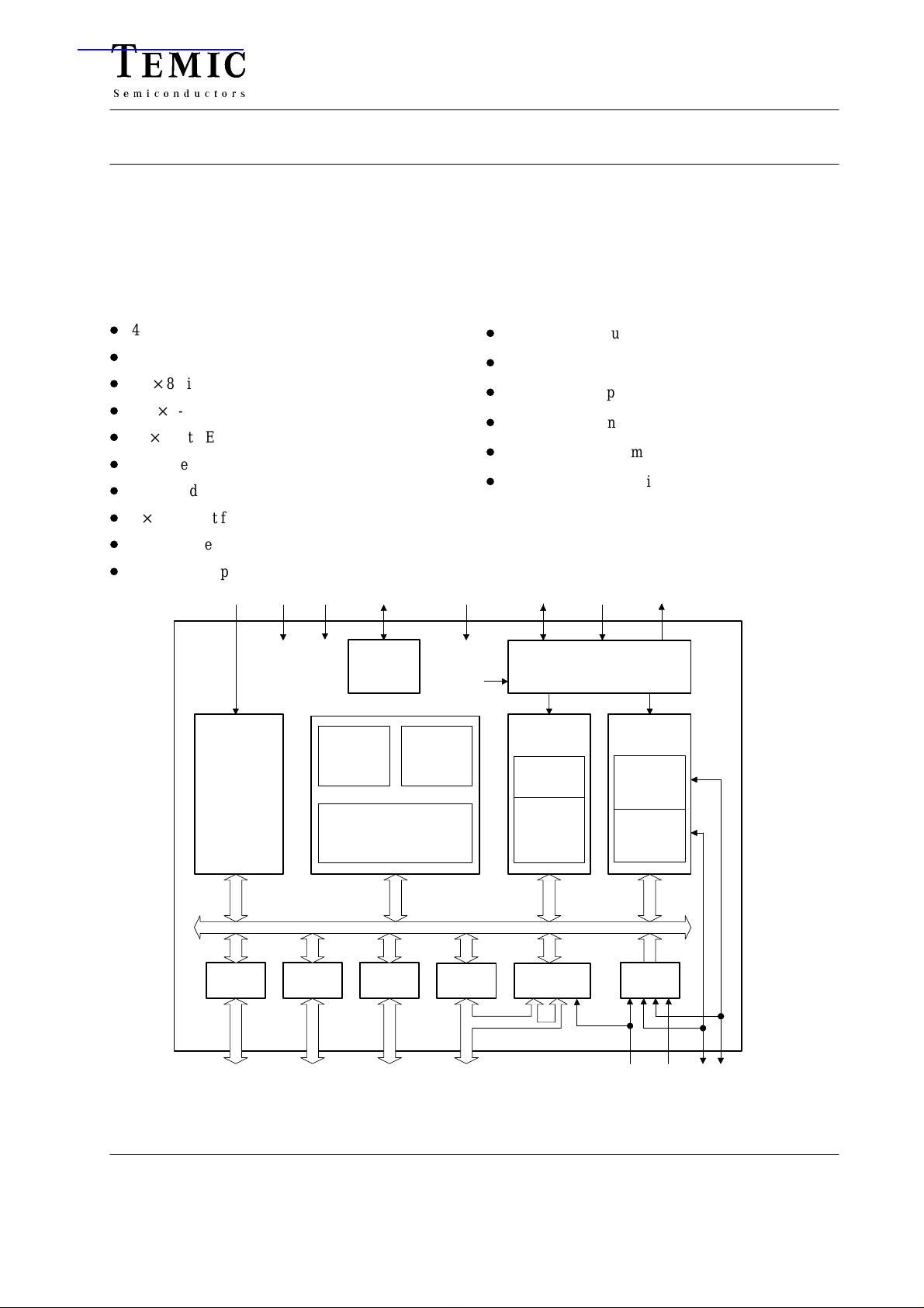
Features
D
4-bit HARVARD architecture
D
1 µs instruction cycle
D
4K 8-bit application program memory
D
256 4-bit RAM
D16
D
D
D2
D
D
8-bit EEPROM
16 bidirectional I/O’s
8 hard and software interrupt levels
8-bit multifunction timer/counter
Interval timer with watchdog
32 kHz on-chip oscillator
NWP
SS
V
V
EEPROM
16 x 8 bit
DD
NRST
Reset
ROM or
EEPROM
4K x 8 bit
MARC4
4–bit CPU core
Test
Sleep
RAM
256 x 4 bit
Benefits
D
Low power consumption
D
Power-down mode < 1 µA
D
2.4 to 6.2 V supply voltage
D
Self-test functions
D
High-level programming language in qFORTH
D
User programmable with the application program
TE TCL
Timer 1
Watch dog
Intervall
timer
OSCIN OSCOUT
Clock
Timer 2
Timer B
Timer A
I/O bus
IP40
Input
Port 4
IP43
TA
TB
94 9038
I/O
Port 0 Port 1 Port 2 Port 3
I/O I/O I/O
Figure 1. Block diagram
Interrupt
inputs
INT6
Rev . A2, 01-Oct-98 1 (51)
M44C260/M48C260
Á
Á
Á
Á
Á
Á
Á
Á
Á
Á
BP02
BP03
NWP
TE
OSC OUT
OSC IN
VDD
NRST
BP20
BP21
BP22
BP23
BP10
BP11
1
2
3
4
5
M44C260
6
7
M48C260
8
9
10
11
12
13
14 15
BP01
28
BP00
27
BP33
26
BP32
25
BP31
24
23
BP30
VSS
22
TCL
21
20
IP40–INT6
IP41–TA
19
IP42–TB
18
IP43
17
BP13
16
BP12
94 9039
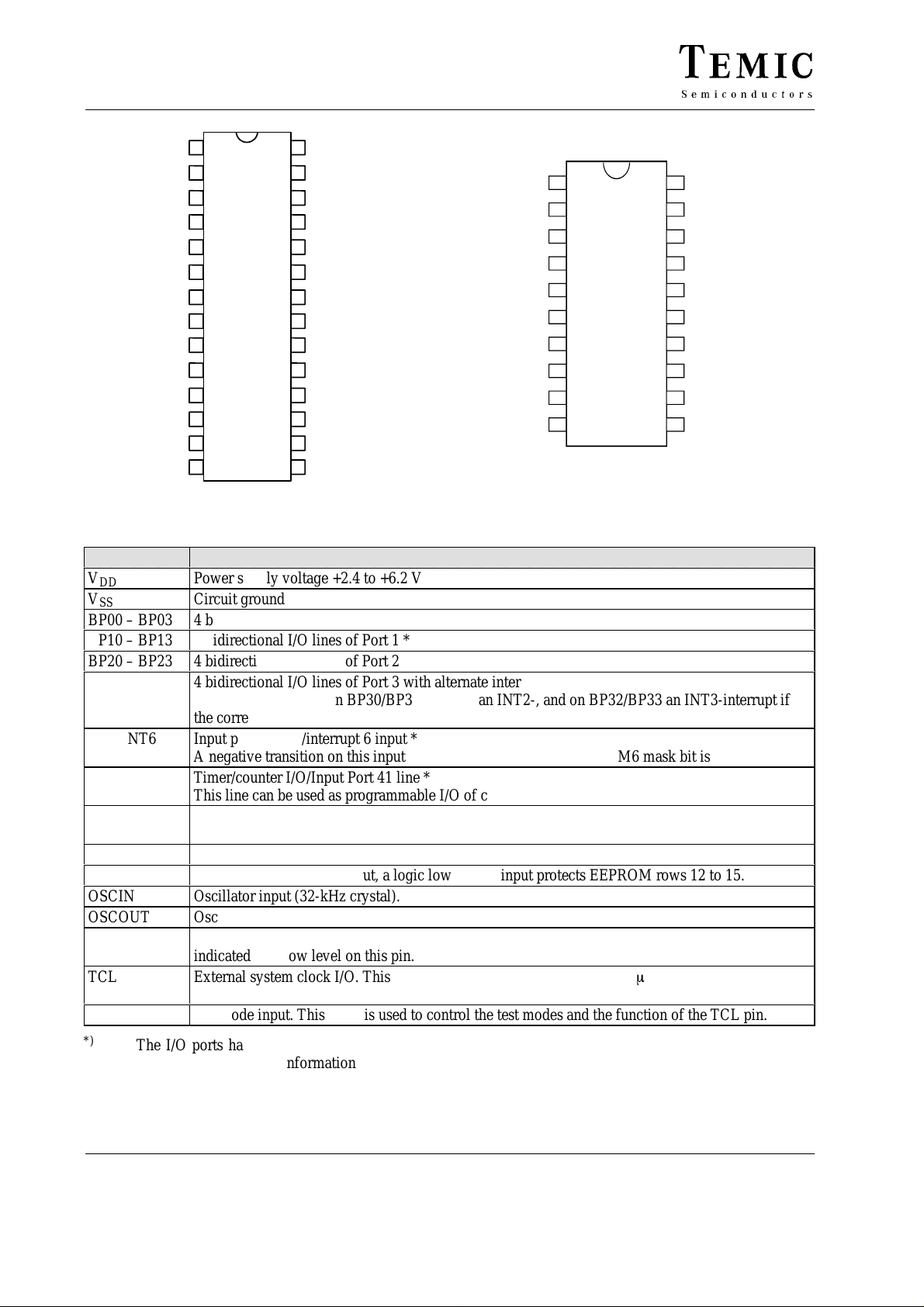
Figure 2. Pin connections for SSO28–FN
Table 1. Pin description
Name Function
V
DD
V
SS
BP00 – BP03
BP10 – BP13
BP20 – BP23
BP30 – BP33
ÁÁÁ
IP40-INT6
ÁÁÁ
IP41-TA
Power supply voltage +2.4 to +6.2 V
Circuit ground
4 bidirectional I/O lines of Port 0 *
4 bidirectional I/O lines of Port 1 *
4 bidirectional I/O lines of Port 2
4 bidirectional I/O lines of Port 3 with alternate interrupt function.
A negative transition on BP30/BP31 requests an INT2-, and on BP32/BP33 an INT3-interrupt if
ББББББББББББББББББББББББББ
the corresponding interrupt-mask is set.
Input port 40 line/interrupt 6 input *
A negative transition on this input requests an INT6 interrupt if the IM6 mask bit is set.
ББББББББББББББББББББББББББ
Timer/counter I/O/Input Port 41 line *
This line can be used as programmable I/O of counter A or as Port 41 input.
IP42-TB
ÁÁÁ
IP43
NWP
OSCIN
OSCOUT
NRST
ÁÁÁ
TCL
ÁÁÁ
TE
*)
The I/O ports have CMOS output buffers. As input they are available with pull-up or pull-down resistors.
Timer/counter I/O/input Port 42 line *
ББББББББББББББББББББББББББ
This line can be used as programmable I/O of counter B or as Port 42 input.
Input Port 43 line
*)
EEPROM write protect input, a logic low on this input protects EEPROM rows 12 to 15.
Oscillator input (32-kHz crystal).
Oscillator output (32-kHz crystal).
Reset input/output, a logic low on this pin resets the device. An internal watchdog reset is
ББББББББББББББББББББББББББ
indicated by a low level on this pin.
External system clock I/O. This pin can be used as input to provide the mC with an external
clock or as output of the internal system clock.
ББББББББББББББББББББББББББ
T estmode input. This input is used to control the test modes and the function of the TCL pin.
Please see the ordering information.
1
BP02
BP03
2
TE
3
VDD
NRST
BP20
BP10
BP11
4
5
M44C260
6
7
8
9
10
OSC OUT
OSC IN
Figure 3. Pin connections for SSO20
20
BP01
19
BP00
BP31
18
BP30
17
16
VSS
TCL
15
INT6
–IP40
14
–IP
TA
13
12
11
41
BP13
BP12
Rev . A2, 01-Oct-982 (51)

M44C260/M48C260
Contents
1 MARC4 Architecture 5. . . . . . . . . . . . . . . . . . . . . . . . . . . . . . . . . . . . . . . . . . . . . . . . . . . . . . . . . . . . . . .
1.1 General Description 5. . . . . . . . . . . . . . . . . . . . . . . . . . . . . . . . . . . . . . . . . . . . . . . . . . . . . . . . . .
1.2 Components of MARC4 Core 5. . . . . . . . . . . . . . . . . . . . . . . . . . . . . . . . . . . . . . . . . . . . . . . . . .
1.2.1 Program Memory (ROM or EEPROM) 5. . . . . . . . . . . . . . . . . . . . . . . . . . . . . . . . . .
1.2.2 Data Memory (RAM) 6. . . . . . . . . . . . . . . . . . . . . . . . . . . . . . . . . . . . . . . . . . . . . . . .
1.2.3 Registers 7. . . . . . . . . . . . . . . . . . . . . . . . . . . . . . . . . . . . . . . . . . . . . . . . . . . . . . . . . .
1.2.4 ALU 8. . . . . . . . . . . . . . . . . . . . . . . . . . . . . . . . . . . . . . . . . . . . . . . . . . . . . . . . . . . . .
1.2.5 Self-Check 8. . . . . . . . . . . . . . . . . . . . . . . . . . . . . . . . . . . . . . . . . . . . . . . . . . . . . . . .
1.2.6 Instruction Cycles 8. . . . . . . . . . . . . . . . . . . . . . . . . . . . . . . . . . . . . . . . . . . . . . . . . . .
1.2.7 I/O Bus 8. . . . . . . . . . . . . . . . . . . . . . . . . . . . . . . . . . . . . . . . . . . . . . . . . . . . . . . . . . .
1.2.8 Interrupt Structure 9. . . . . . . . . . . . . . . . . . . . . . . . . . . . . . . . . . . . . . . . . . . . . . . . . . .
Software Interrupts 10. . . . . . . . . . . . . . . . . . . . . . . . . . . . . . . . . . . . . . . . . . . . . . . . . .
Hardware Interrupts 10. . . . . . . . . . . . . . . . . . . . . . . . . . . . . . . . . . . . . . . . . . . . . . . . .
1.3 Reset 10. . . . . . . . . . . . . . . . . . . . . . . . . . . . . . . . . . . . . . . . . . . . . . . . . . . . . . . . . . . . . . . . . . . . . .
1.4 Clock Generation 11. . . . . . . . . . . . . . . . . . . . . . . . . . . . . . . . . . . . . . . . . . . . . . . . . . . . . . . . . . . .
1.4.1 Clock Status/Control Register (CSC) 12. . . . . . . . . . . . . . . . . . . . . . . . . . . . . . . . . . . .
1.4.2 TCL Signal 12. . . . . . . . . . . . . . . . . . . . . . . . . . . . . . . . . . . . . . . . . . . . . . . . . . . . . . . .
1.5 Power Down Modes 12. . . . . . . . . . . . . . . . . . . . . . . . . . . . . . . . . . . . . . . . . . . . . . . . . . . . . . . . . .
2 Peripheral Modules 13. . . . . . . . . . . . . . . . . . . . . . . . . . . . . . . . . . . . . . . . . . . . . . . . . . . . . . . . . . . . . . . .
2.1 Addressing Peripherals 13. . . . . . . . . . . . . . . . . . . . . . . . . . . . . . . . . . . . . . . . . . . . . . . . . . . . . . . .
2.1.1 Input Port 4 15. . . . . . . . . . . . . . . . . . . . . . . . . . . . . . . . . . . . . . . . . . . . . . . . . . . . . . . .
2.1.2 Bidirectional Ports 15. . . . . . . . . . . . . . . . . . . . . . . . . . . . . . . . . . . . . . . . . . . . . . . . . .
2.1.3 External Interrupt Inputs 16. . . . . . . . . . . . . . . . . . . . . . . . . . . . . . . . . . . . . . . . . . . . . .
2.2 Timer 1 17. . . . . . . . . . . . . . . . . . . . . . . . . . . . . . . . . . . . . . . . . . . . . . . . . . . . . . . . . . . . . . . . . . . .
2.2.1 T1C – Timer 1 Control Register 18. . . . . . . . . . . . . . . . . . . . . . . . . . . . . . . . . . . . . . . .
2.2.2 WDC – Watchdog Control Register 18. . . . . . . . . . . . . . . . . . . . . . . . . . . . . . . . . . . . .
2.3 Timer 2 19. . . . . . . . . . . . . . . . . . . . . . . . . . . . . . . . . . . . . . . . . . . . . . . . . . . . . . . . . . . . . . . . . . . .
2.3.1 Timer 2 Status/Control Register (T2SC) 21. . . . . . . . . . . . . . . . . . . . . . . . . . . . . . . . .
2.3.2 Timer 2 Subport (T2SUB) 22. . . . . . . . . . . . . . . . . . . . . . . . . . . . . . . . . . . . . . . . . . . .
2.3.3 Timer 2 Reload Register 22. . . . . . . . . . . . . . . . . . . . . . . . . . . . . . . . . . . . . . . . . . . . . .
2.3.4 Timer 2 Capture Register 23. . . . . . . . . . . . . . . . . . . . . . . . . . . . . . . . . . . . . . . . . . . . .
2.3.5 Timer A Mode Register 1 (TAM1) 23. . . . . . . . . . . . . . . . . . . . . . . . . . . . . . . . . . . . . .
2.3.6 Timer A Mode Register 2 (TAM2) 24. . . . . . . . . . . . . . . . . . . . . . . . . . . . . . . . . . . . . .
2.3.7 Timer B Mode Register 1 (TBM1) 24. . . . . . . . . . . . . . . . . . . . . . . . . . . . . . . . . . . . . .
2.3.8 Timer B Mode Register 2 (TBM2) 25. . . . . . . . . . . . . . . . . . . . . . . . . . . . . . . . . . . . . .
2.3.9 Timer 2 Prescaler Control Register (T2PC) 25. . . . . . . . . . . . . . . . . . . . . . . . . . . . . . .
2.3.10 Timer 2 Interrupt Control Register (T2IC) 26. . . . . . . . . . . . . . . . . . . . . . . . . . . . . . . .
2.3.11 Timer I/O (TA/TB) 27. . . . . . . . . . . . . . . . . . . . . . . . . . . . . . . . . . . . . . . . . . . . . . . . . .
2.4 EEPROM 28. . . . . . . . . . . . . . . . . . . . . . . . . . . . . . . . . . . . . . . . . . . . . . . . . . . . . . . . . . . . . . . . . .
2.4.1 EEPROM SubPort (ESUB) 28. . . . . . . . . . . . . . . . . . . . . . . . . . . . . . . . . . . . . . . . . . .
2.4.2 EEPROM Mode/Status Register (EMS) 29. . . . . . . . . . . . . . . . . . . . . . . . . . . . . . . . . .
Rev . A2, 01-Oct-98 3 (51)

M44C260/M48C260
Contents (continued)
3 Appendix 30. . . . . . . . . . . . . . . . . . . . . . . . . . . . . . . . . . . . . . . . . . . . . . . . . . . . . . . . . . . . . . . . . . . . . . . . .
3.1 Emulation 30. . . . . . . . . . . . . . . . . . . . . . . . . . . . . . . . . . . . . . . . . . . . . . . . . . . . . . . . . . . . . . . . . .
3.2 Programming the EEPROM Program Memory 30. . . . . . . . . . . . . . . . . . . . . . . . . . . . . . . . . . . . .
3.3 MARC4 Instruction Set 30. . . . . . . . . . . . . . . . . . . . . . . . . . . . . . . . . . . . . . . . . . . . . . . . . . . . . . .
3.3.1 MARC4 Instruction Set Overview 31. . . . . . . . . . . . . . . . . . . . . . . . . . . . . . . . . . . . . .
3.3.2 qFOR TH Language Overview 32. . . . . . . . . . . . . . . . . . . . . . . . . . . . . . . . . . . . . . . . .
3.4 The qFORTH Language - Quick Reference Guide 33. . . . . . . . . . . . . . . . . . . . . . . . . . . . . . . . . .
3.4.1 Arithmetic/Logical 33. . . . . . . . . . . . . . . . . . . . . . . . . . . . . . . . . . . . . . . . . . . . . . . . . .
3.4.2 Comparisons 33. . . . . . . . . . . . . . . . . . . . . . . . . . . . . . . . . . . . . . . . . . . . . . . . . . . . . . .
3.4.3 Control Structures 34. . . . . . . . . . . . . . . . . . . . . . . . . . . . . . . . . . . . . . . . . . . . . . . . . . .
3.4.4 Stack Operations 34. . . . . . . . . . . . . . . . . . . . . . . . . . . . . . . . . . . . . . . . . . . . . . . . . . . .
3.4.5 Memory Operations 35. . . . . . . . . . . . . . . . . . . . . . . . . . . . . . . . . . . . . . . . . . . . . . . . .
3.4.6 Predefined Structures 36. . . . . . . . . . . . . . . . . . . . . . . . . . . . . . . . . . . . . . . . . . . . . . . .
3.4.7 Assembler Mnemonics 36. . . . . . . . . . . . . . . . . . . . . . . . . . . . . . . . . . . . . . . . . . . . . . .
4 Electrical Characteristics 38. . . . . . . . . . . . . . . . . . . . . . . . . . . . . . . . . . . . . . . . . . . . . . . . . . . . . . . . . . . .
4.1 Absolute Maximum Ratings 38. . . . . . . . . . . . . . . . . . . . . . . . . . . . . . . . . . . . . . . . . . . . . . . . . . . .
4.2 DC Operating Characteristics 38. . . . . . . . . . . . . . . . . . . . . . . . . . . . . . . . . . . . . . . . . . . . . . . . . . .
4.3 AC Characteristics 39. . . . . . . . . . . . . . . . . . . . . . . . . . . . . . . . . . . . . . . . . . . . . . . . . . . . . . . . . . .
4.4 Schmitt-Trigger Inputs 45. . . . . . . . . . . . . . . . . . . . . . . . . . . . . . . . . . . . . . . . . . . . . . . . . . . . . . . .
5 Pad Layout 46. . . . . . . . . . . . . . . . . . . . . . . . . . . . . . . . . . . . . . . . . . . . . . . . . . . . . . . . . . . . . . . . . . . . . . .
6 Package Information 48. . . . . . . . . . . . . . . . . . . . . . . . . . . . . . . . . . . . . . . . . . . . . . . . . . . . . . . . . . . . . . .
7 Standard Design of M48C260 49. . . . . . . . . . . . . . . . . . . . . . . . . . . . . . . . . . . . . . . . . . . . . . . . . . . . . . . .
8 Ordering Information for M44C260 50. . . . . . . . . . . . . . . . . . . . . . . . . . . . . . . . . . . . . . . . . . . . . . . . . .
Rev . A2, 01-Oct-984 (51)
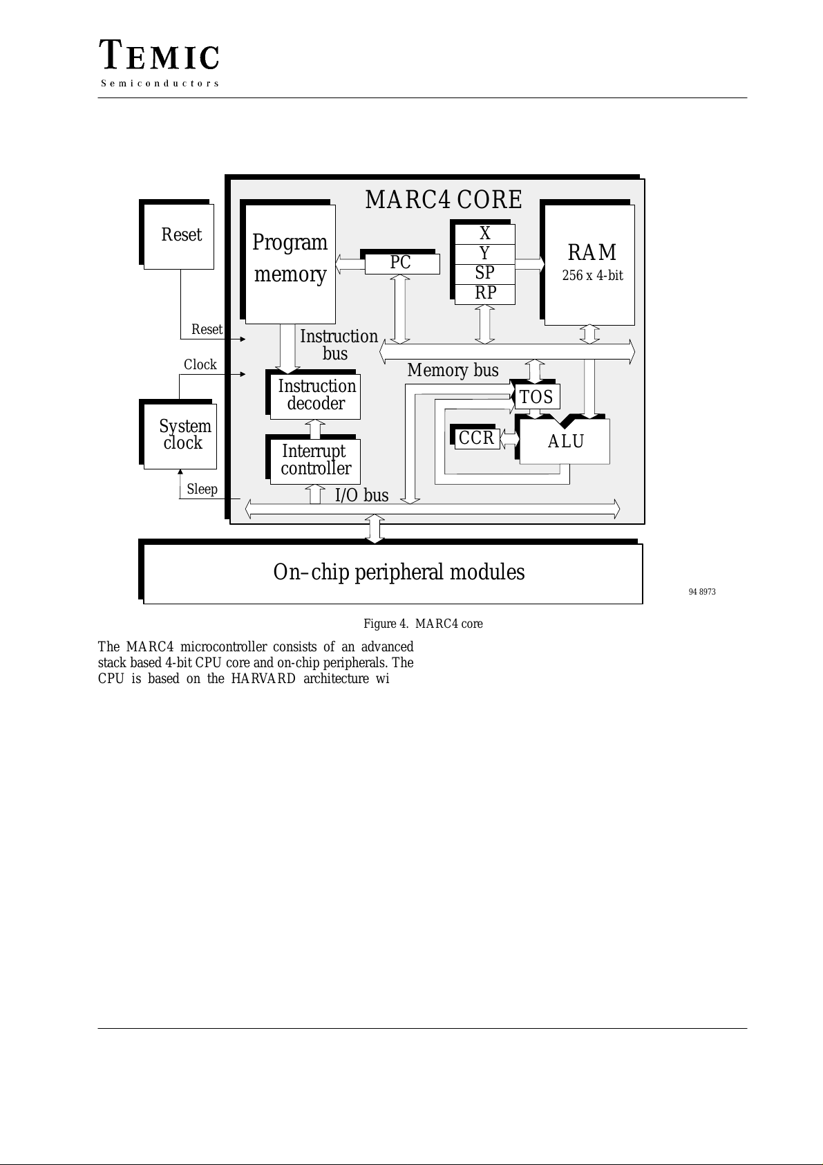
1 MARC4 Architecture
1.1 General Description
M44C260/M48C260
MARC4 CORE
Reset
Program
PC
memory
Reset
Clock
System
clock
Sleep
Instruction
bus
Instruction
decoder
Interrupt
controller
I/O bus
On–chip peripheral modules
Figure 4. MARC4 core
The MARC4 microcontroller consists of an advanced
stack based 4-bit CPU core and on-chip peripherals. The
CPU is based on the HARVARD architecture with a
physically separate program memory (ROM or
EEPROM) and data memory (RAM). Three independent
buses the instruction bus, the memory bus and the I/O bus
are used for parallel communication between program
memory, RAM and peripherals. This enhances program
execution speed by allowing both instruction prefetching,
and simultaneous communication to the on-chip peripheral circuitry. The integrated powerful interrupt
controller with eight prioritized interrupt levels, supports
fast processing of hardware events.
The MARC4 is designed for the high level programming
language qFORTH. The core contains both FORTH
stacks, expression stack and return stack. This architecture allows high level language programming without any
loss in efficiency or code density.
1.2 Components of MARC4 Core
The core contains a program memory, RAM, ALU, program counter, RAM address register, instruction decoder
X
Y
SP
RAM
256 x 4-bit
RP
Memory bus
TOS
CCR
and interrupt controller. The following sections describe
each of these parts.
1.2.1 Program Memory (ROM or
EEPROM)
The ROM is mask programmed with the application program during the fabrication of the microcontroller. The
EEPROM is programmed by the customer using a special
programming device (see chapter ”Progamming the
EEPROM Program Memory”). The program memory is
addressed by a 12-bit wide program counter, thus limiting
the program size to a maximum of 4 Kbytes. The
M44C260 contains an additional 1 Kbyte ROM for test
software. The program memory starts with a 512 byte segment (zero page) which contains predefined start
addresses for interrupt service routines and special subroutines accessible with single byte instructions
(SCALL). The corresponding memory map is shown in
the figure 4.Look-up tables of constants can also be held
in the program memory and are accessed via the
MARC4’s built-in TABLE instruction.
ALU
94 8973
Rev . A2, 01-Oct-98 5 (51)
M44C260/M48C260
FFFh
Program
memory
(4K x 8-bit)
Self test
bank (1K)
only
1FFh
M44C260
Zero page
000h
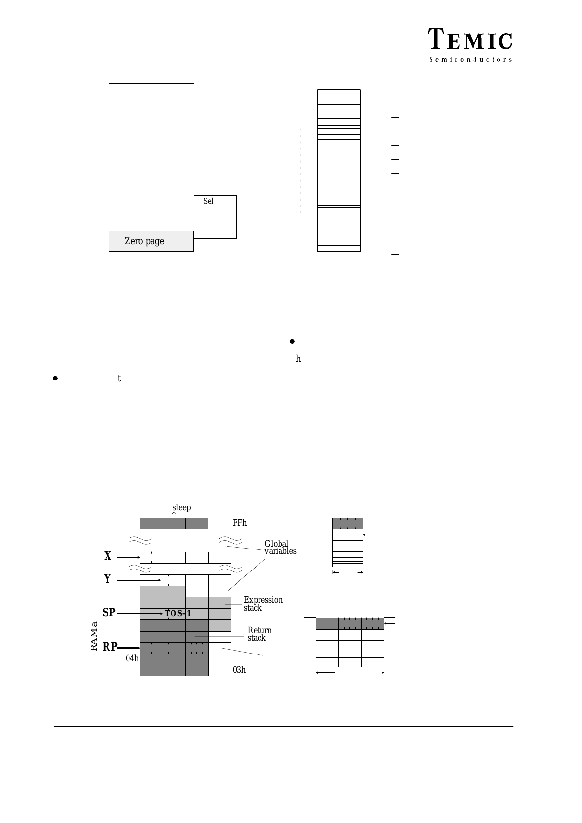
1.2.2 Data Memory (RAM)
The MARC4 contains a 256 x 4-bit wide static random access memory (RAM). It is used for the expression stack,
the return stack and data memory for variables and arrays.
The RAM is addressed by any of the four 8-bit wide RAM
address registers SP, RP, X and Y.
D
Expression Stack
The 4-bit wide expression stack is addressed with the expression stack pointer (SP). All arithmetic, I/O and
memory reference operations take their operands from,
and return their result to the expression stack. The
MARC4 performs the operations with the top of stack
items (TOS and TOS-1). The TOS register contains the
3FFh
000h
Figure 5. Program memory map
1F8h
1F0h
1E8h
1E0h
SCALL addresses
020h
018h
010h
008h
000h
Zero
page
1E0h
1C0h
180h
140h
100h
0C0h
080h
040h
008h
000h
INT7
INT6
INT5
INT4
INT3
INT2
INT1
INT0
$RESET
$AUTOSLEEP
94 8974
top element of the expression stack and works like an
accumulator. This stack is also used for passing parameters between subroutines, and as a scratchpad area for
temporary storage of data.
D
Return Stack
The 12-bit wide return stack is addressed by the return
stack pointer (RP). It is used for storing return addresses
of subroutines, interrupt routines and for keeping loop index counts. The return stack can also be used as a
temporary storage area.
The MARC4 instruction set supports the exchange of data
between the top elements of the expression stack and the
return stack. The two stacks within the RAM have a user
definable location and maximum depth.
RAM
(256 x 4-bit)
Autosleep
FCh
X
Y
SP
RP
RAM address register:
04h
00h
TOS–1
FFh
Global
variables
Expression
stack
Return
stack
Global
07h
03h
v
variables
Figure 6. RAM map
Expression stack
30
TOS
TOS–1
TOS–2
4-bit
SP
Return stack
11
12-bit
0
RP
94 8975
Rev . A2, 01-Oct-986 (51)
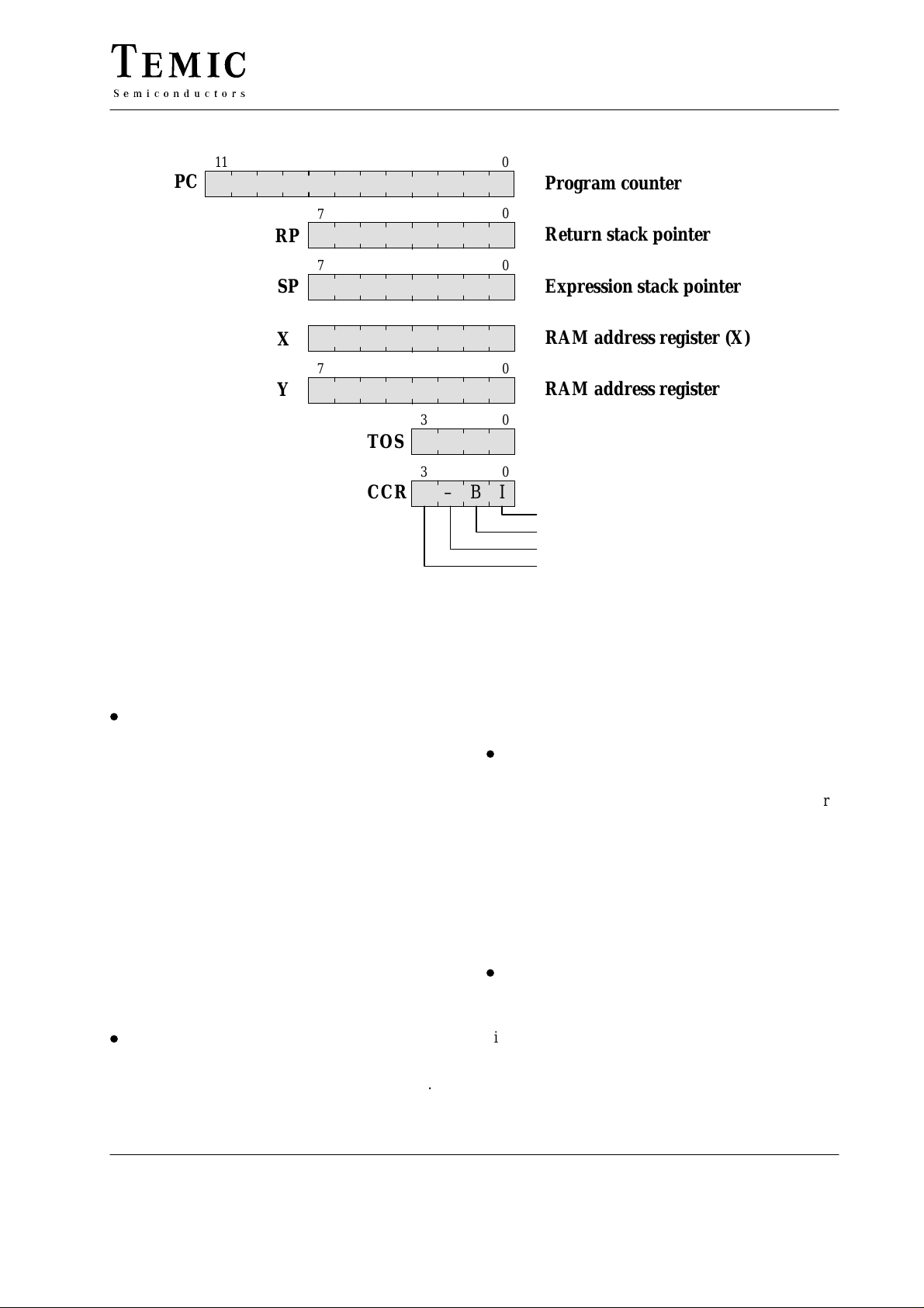
1.2.3 Registers
11
PC
M44C260/M48C260
0
Program counter
7
RP
7
SP
7
X
Y
3
TOS
3
CCR
The MARC4 controller has six programmable registers
and one condition code register. They are shown in
figure 7.
D
Program Counter (PC)
The program counter (PC) is a 12-bit register that contains
the address of the next instruction to be fetched from the
program memory. Instructions currently being executed
are decoded in the instruction decoder to determine the
internal micro operations. For linear code (no calls or
branches) the program counter is incremented with every
instruction cycle. If a branch-, call-, return-instruction or
an interrupt is executed the program counter is loaded
with a new address. The program counter is also used with
the TABLE instruction to fetch 8-bit wide ROM
constants.
RAM Address Register
The RAM is addressed with the four 8-bit wide RAM
address registers: SP, RP, X and Y. These registers allow
access to any of the 256 RAM nibbles.
D
Expression Stack Pointer (SP)
The stack pointer (SP) contains the address of the next-totop 4-bit item (TOS-1) of the expression stack. The
pointer is automatically pre-incremented if a nibble is
moved onto the stack, or post-decremented if a nibble is
C
–
Figure 7. Programming model
0
00
Return stack pointer
0
Expression stack pointer
0
RAM address register (X)
07
RAM address register (Y)
0
Top of stack register
0
B
I
Condition code register
Interrupt enable
Branch
Unused
Carry / borrow
removed from the stack. Every post-decrement operation
moves the item (TOS-1) to the TOS register before the SP
is decremented. After a reset, the stack pointer has to be
initialized with ” >SP $xx ” to allocate the start address
of the expression stack area.
D
Return Stack Pointer (RP)
The return stack pointer points to the top element of the
12-bit wide return stack. The pointer automatically preincrements if an element is moved onto the stack or it
post-decrements if an element is removed from the stack.
The return stack pointer increments and decrements in
steps of 4. This means that every time a 12-bit element is
stacked, a 4-bit RAM location is left unwritten. This location is used by the qFORTH compiler to allocate 4-bit
variables. After a reset the return stack pointer has to be
initialized with ” >RP FCh ”.
D
RAM Address Register (X and Y)
The X and Y registers are used to address any 4-bit item
in the RAM. A fetch operation moves the addressed
nibble onto the TOS. A store operation moves the TOS to
the addressed RAM location. By using either the pre-increment or post-decrement addressing mode arrays in the
RAM can be compared, filled or moved.
94 8976
Rev . A2, 01-Oct-98 7 (51)
M44C260/M48C260
D
T op Of Stack (TOS)
The top of stack register is the accumulator of the
MARC4. All arithmetic/logic, memory reference and I/O
operations use this register . The TOS register gets the data
from the ALU, the program memory, the RAM or via the
I/O bus.
D
Condition Code Register (CCR)
The 4-bit wide condition code register contains the
branch, the carry and the interrupt enable flag. These bits
indicate the current state of the CPU. The CCR flags are
set or reset by ALU operations. The instructions
SET_BCF, TOG_BF, CCR! and DI allow a direct
manipulation of the condition code register .
Carry/Borrow (C)
The carry/borrow flag indicates that borrow or carry out
of arithmetic logic unit (ALU) occurred during the last
arithmetic operation. During shift and rotate operations
this bit is used as a fifth bit. Boolean operations have no
affect on the C flag.
Branch (B)
The branch flag controls the conditional program branching. When the branch flag has been set by one of the
previous instructions a conditional branch is taken. This
flag is affected by arithmetic, logic, shift, and rotate operations.
Interrupt Enable (I)
The interrupt enable flag enables or disables the interrupt
processing on a global basis. After reset or by executing
the DI instruction, the interrupt enable flag is reset and all
interrupts are disabled. The µC does not process further
interrupt requests until the interrupt enable flag is set
again by either executing an EI, RTI or SLEEP
instruction.
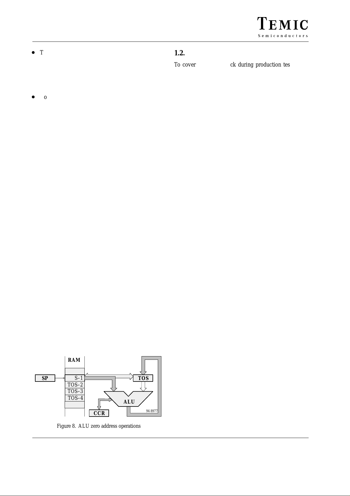
1.2.4 ALU
The 4-bit ALU performs all the arithmetic, logical, shift
and rotate operations with the top two elements of the
expression stack (TOS and TOS-1) and returns its result
to the TOS. The ALU operations affect the carry/borrow
and branch flag in the condition code register (CCR).
RAM
SP
TOS–1
TOS–2
TOS–3
TOS–4
CCR
Figure 8. ALU zero address operations
ALU
TOS
94 8977
1.2.5 Self-Check
To cover the ROM block during production testing the
ROM_TEST2 routine has to be included into the $RESET
routine.
: $RESET >SP S0
>RP FCh
Port7 IN Fh =
IF ROM_Test2
THEN
\*** main program
;
Note: The corresponding file ROM_TEST.INC has to
be included into the project’s main file. The
conditional execution is stimulated during the
production test.
1.2.6 Instruction Cycles
A MARC4 instruction word is one or two bytes long and
is executed within one or four machine-cycles. A
machine-cycle consists of two system clocks (SYSCL).
The MARC4 is a zero address machine. Most of the
instructions are one byte long and are executed only in
one machine-cycle. The CPU has an instruction pipeline,
which allows the controller to fetch the next instruction
from program memory at the same time as the present
instruction is being executed. For more information see
the section ”MARC4 Instruction Set Overview”.
1.2.7 I/O Bus
The I/O ports and the registers of the peripheral modules
(Timer 1, Timer 2, EEPROM) are I/O mapped. The communication between the core and the on-chip peripherals
takes place via the I/O bus and the associated I/O control
bus. These buses are used for different functions: for read
and write accesses, for the interrupt generation, to reset
peripherals and for the SLEEP mode. With the MARC4
IN-instruction and OUT-instruction the I/O bus allows a
direct read or write access to one of the 16 I/O addresses.
More about the I/O access to the on-chip peripherals is
described in the section ”Peripheral modules”.
The I/O buses are internal buses and are not accessible by
the customer on the final microcontroller device, but they
are used as the interface for the MARC4 emulation (see
also the section “Emulation”).
Rev . A2, 01-Oct-988 (51)
M44C260/M48C260
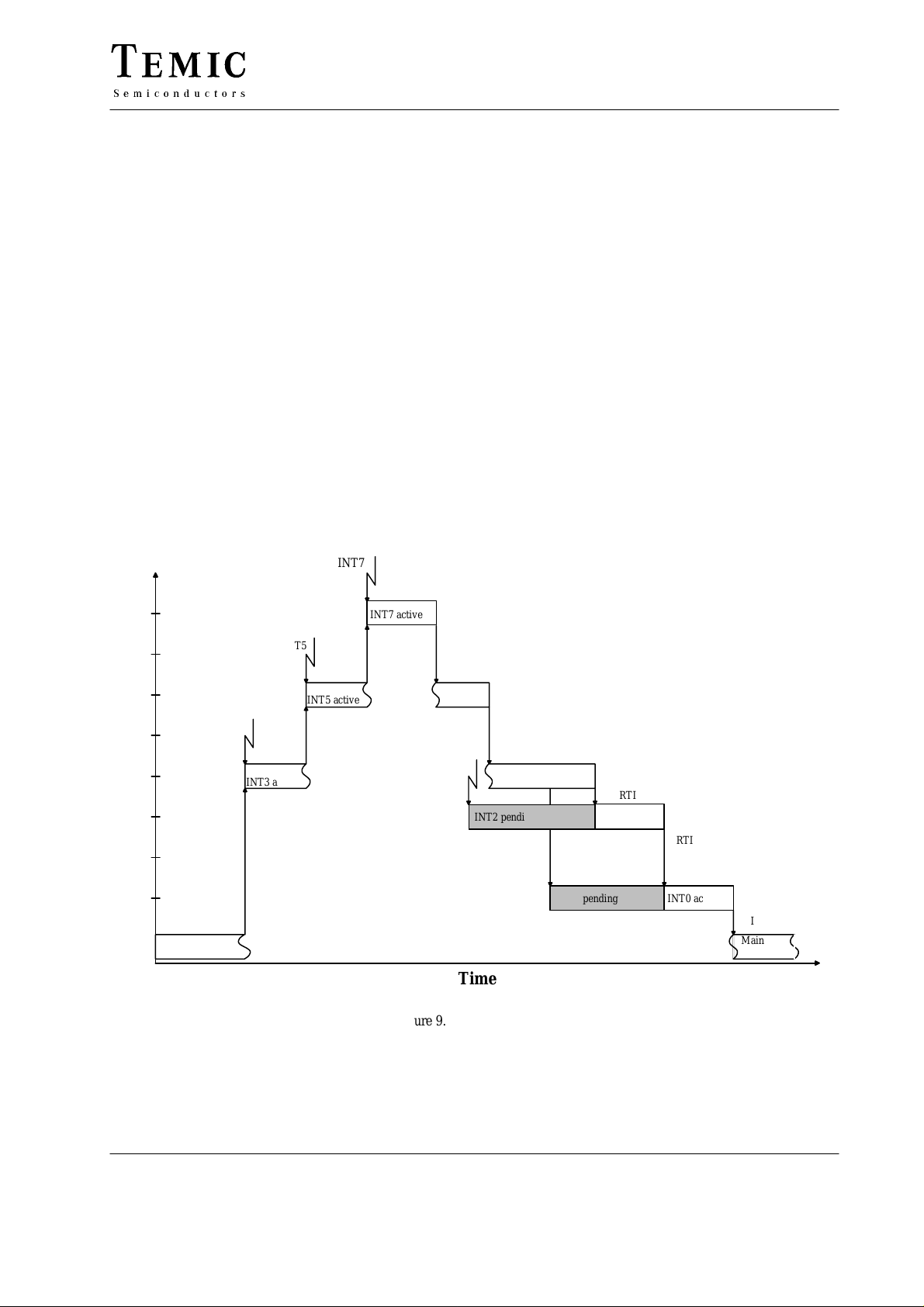
1.2.8 Interrupt Structure
The MARC4 can handle interrupts with eight different
priority levels. They can be generated from the internal
and external interrupt sources or by a software interrupt
from the CPU itself. Each interrupt level has a hard-wired
priority and an associated vector for the service routine in
the ROM (see table 2). The programmer can enable or disable interrupts all together by setting or resetting the
interrupt enable flag (I) in the CCR.
Interrupt Processing
For processing the eight interrupt levels, the MARC4
contains an interrupt controller with the 8-bit wide interrupt pending and interrupt active register. The interrupt
controller samples all interrupt requests during every
non-I/O instruction cycle and latches them in the interrupt
pending register. If no higher priority interrupt is present
in the interrupt active register it signals the CPU to interrupt the current program execution. If the interrupt enable
bit is set the processor enters an interrupt acknowledge
cycle. During this cycle a SHORT CALL instruction to
INT7
the service routine is executed and the current PC is saved
on the return stack. An interrupt service routine is finished
with the RTI instruction. This instruction sets the interrupt
enable flag, resets the corresponding bits in the interrupt
pending/active register and fetches the return address
from the return stack to the program counter. When the
interrupt enable flag is reset (interrupts are disabled), the
execution of interrupts is inhibited but not the logging of
the interrupt requests in the interrupt pending register.
The execution of the interrupt will be delayed until the
interrupt enable flag is set again. But note that interrupts
are lost if an interrupt request occurs during the corresponding bit in the pending register is still set. After the
reset (power-on, external or watchdog reset), the interrupt
enable flag and the interrupt pending and interrupt active
register are reset.
Interrupt Latency
The interrupt latency is the time from the falling edge of
the interrupt to the interrupt service routine being
activated. In the MARC4 this takes between 3 to 5
machine cycles depending on the state of the core.
7
6
5
4
3
Priority level
2
1
0
Main /
Autosleep
INT3
INT5
INT3 active
INT5 active
INT7 active
RTI
INT2
INT2 pending
Time
Figure 9. Interrupt handling
RTI
SWI0
INT2 active
INT0 pending
RTI
RTI
INT0 active
RTI
Main /
Autosleep
94 8978
Rev . A2, 01-Oct-98 9 (51)
M44C260/M48C260
Á
Á
Á
Á
Á
Á
Á
Á
Á
Á
Á
Á
Á
Á
Á
Á
Á
Á
Á
Á
Á
Á
Á
Á
Á
Á
Á
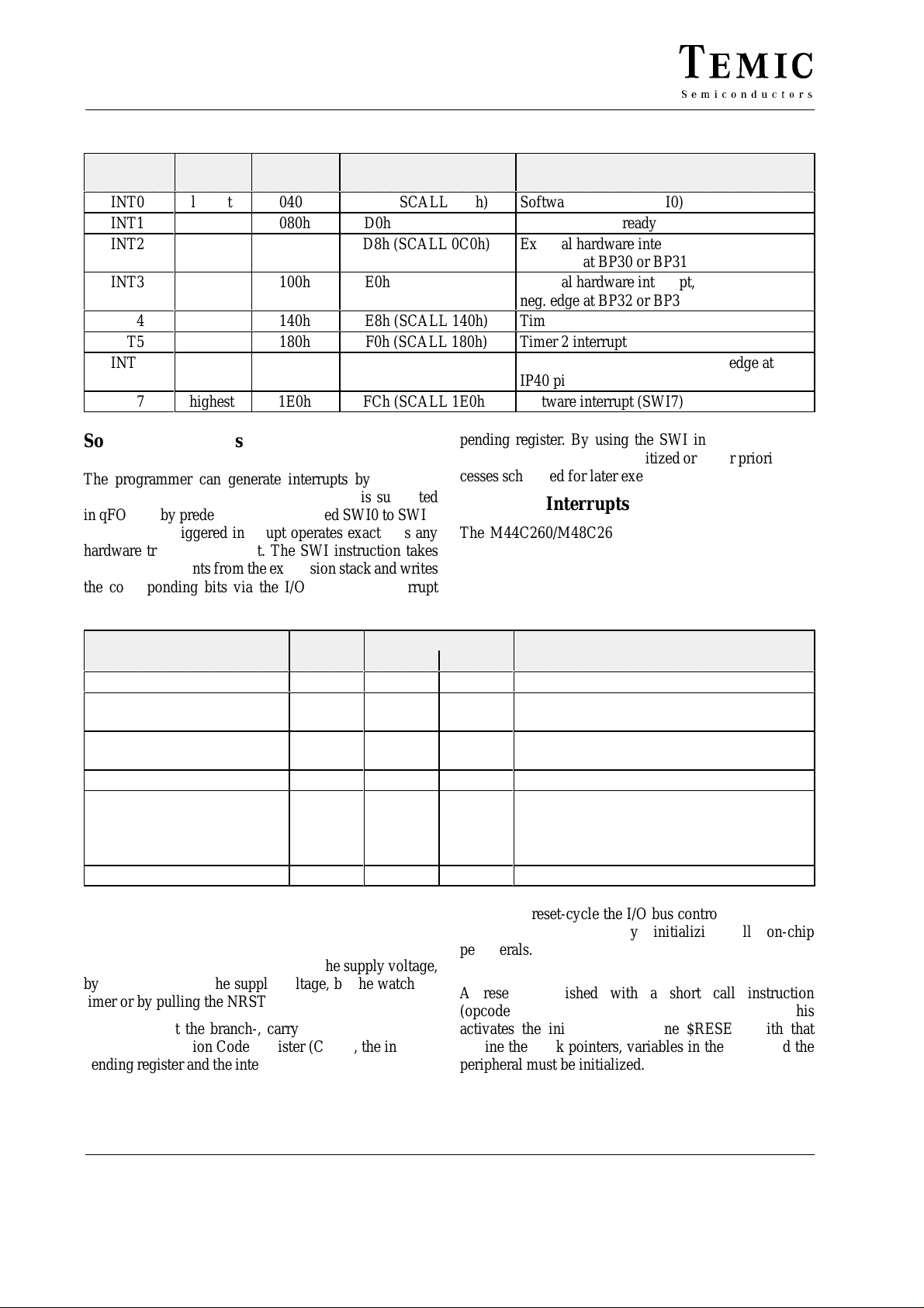
Table 2. Interrupt priority table
Interrupt Priority Vector
Address
INT0
INT1
INT2
ÁÁÁ
INT3
ÁÁÁ
INT4
INT5
INT6
ÁÁÁ
INT7
lowest
040h
080h
0C0h
ÁÁÁÁÁÁ
100h
ÁÁÁÁÁÁ
140h
180h
1C0h
ÁÁÁÁÁÁ
highest
1E0h
Interrupt Opcode
(Acknowledge)
C8h (SCALL 040h)
D0h (SCALL 080h)
D8h (SCALL 0C0h)
ББББББ
E0h (SCALL 100h)
ББББББ
E8h (SCALL 140h)
F0h (SCALL 180h)
F8h (SCALL 1C0h)
ББББББ
FCh (SCALL 1E0h)
Function
Software interrupt (SWI0)
EEPROM write ready
External hardware interrupt,
ББББББББББББ
neg. edge at BP30 or BP31
External hardware interrupt,
neg. edge at BP32 or BP33
ББББББББББББ
Timer 1 interrupt
Timer 2 interrupt
External hardware interrupt, neg. edge at
ББББББББББББ
IP40 pin
Software interrupt (SWI7)
Software Interrupts
The programmer can generate interrupts by using the
software interrupt instruction (SWI) which is supported
in qFORTH by predefined macros named SWI0 to SWI7.
The software triggered interrupt operates exactly as any
hardware triggered interrupt. The SWI instruction takes
the top two elements from the expression stack and writes
the corresponding bits via the I/O bus to the interrupt
Table 3. Hardware interrupts
Interrupt Priority Mask Interrupt Source
Register Bit
EEPROM write ready
External interrupt
Port 3 (BP30 OR BP31)
External interrupt
ББББББББ
Port 3 (BP32 OR BP33)
Timer 1 interrupt
Timer 2 interrupt
ББББББББ
ББББББББ
Ext. interrupt IP40 input
INT1
INT2
INT3
ÁÁ
INT4
INT5
ÁÁ
ÁÁ
INT6
EMS
IMR1
IMR1
ÁÁ
IMR2
T2IC
ÁÁ
ÁÁ
IMR2
pending register. By using the SWI instruction in thius
way , interrupts can be re-prioritized or lower priority processes scheduled for later execution.
Hardware Interrupts
The M44C260/M48C260 incorporates eleven hardware
interrupt sources with six different levels. Each of these
sources can be enabled or disabled separately with an interrupt mask bit in the IMR1 or IMR2 register.
IMEP
IM30
IM31
IM32
ÁÁ
IM33
IMT1
IMAS
IMAP
ÁÁ
IMBS
ÁÁ
IMBP
IM6
EEPROM end of write cycle
Negative edge at BP30
Negative edge at BP31
Negative edge at BP32
ББББББББББББ
Negative edge at BP33
Timer 1
Timer A end of space/underflow
Timer A end of pulse/capture
ББББББББББББ
Timer B end of space/underflow
ББББББББББББ
Timer B end of pulse/capture
Negative edge at IP40 input
1.3 Reset
The reset puts the CPU into a well-defined condition. The
reset can be triggered by switching on the supply voltage,
by a break-down of the supply voltage, by the watchdog
timer or by pulling the NRST pad to low.
After any reset the branch-, carry- and interrupt enable
flag in the Condition Code Register (CCR) , the interrupt
pending register and the interrupt active register are reset.
During the reset-cycle the I/O bus control signals are set
to ’reset mode’ thereby initializing all on-chip
peripherals.
A reset is finished with a short call instruction
(opcode C1h) to the program memory address 008h. This
activates the initialization routine $RESET. With that
routine the stack pointers, variables in the RAM and the
peripheral must be initialized.
Rev . A2, 01-Oct-9810 (51)
M44C260/M48C260
Power-on Reset
The M44C260/M48C260 incorporates an on-chip
power-on reset (POR) circuitry which provides internal
chip reset for most power-up situations. The power-on
reset ensures that the core is not activated before the operating supply voltage has been reached.
The mC will function normally at > 2.4 V under all conditions. For V
below 2.4 V, the device will either
DD
function normally or the device reset will be globally activated by the brown-out circuit. The actual brown-out trip
point is a function of temperature and process parameters.
External Reset (NRST)
An external reset can be triggered with the NRST pin. For
the external reset the pin should be low for a minimum of
two machine-cycles.
Watchdog Timer Reset
If the watchdog timer function of Timer 1 is enabled, a reset is triggered with every watchdog counter overflow. To
suppress that, the watchdog counter must be reset by an
access to the CWD-register (see also Timer 1/watchdog
counter).
The power-on reset and the watchdog reset are indicated
in the same way as an external reset on the NRST pad.
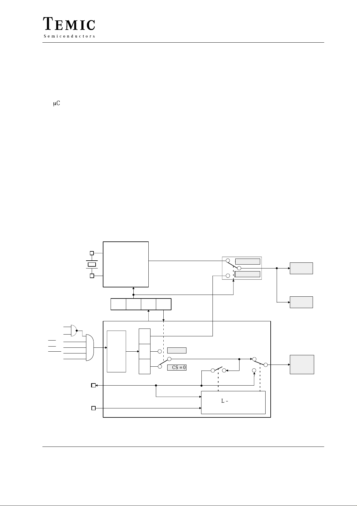
1.4 Clock Generation
The M44C260/M48C260 has two oscillators, one RC oscillator for the system clock generation and an additional
32-kHz crystal oscillator. The system clock generator
provides the core and Timer 2 with the clock. The system
clock frequency is programmable for 1 or 2 MHz. The
crystal oscillator is used as an exact time base for Timer
1. If no exact timing is required, the controller does not
need an external crystal. In this case Timer 1 is provided
with the system clock.
The configuration for both oscillators is programmable
with the clock status control register (CSC), which is a
subport register located in port CSUB. The required configuration has to be initialized after reset in the $RESET
routine. The default setting after a reset is 1 MHz system
clock and an active 32-kHz crystal oscillator.
After power-on or a SLEEP instruction the clock generator needs a start-up time until it runs with an exact timing.
The CRDY bit in the CSC register indicates the start-up
phase.
OSCS
T1R
TAR
TBR
EERDY
SLEEP
OSCIN
Q1
OSCOUT
TCL
TE
CSC :
CSC3
OSC
Stop
OSC32
Stop
OSCS CRDY CCS
/122
/2
/4
f
OSC
= 32 kHz
CCS = 1
CCS = 0
OSCS = 0
OSCS = 1
<= 32 kHz
f
G
Systemclock –
Generator
TCL – Controllogic
CL32
SYSCL
TIMER 1
EEPROM
TIMER 2
CORE
94 8979
Figure 10. Clock module
Rev . A2, 01-Oct-98 11 (51)
M44C260/M48C260
Á
Á
Á
Á
Á
Á
Á
Á
Á
Á
Á
Á
Á
Á
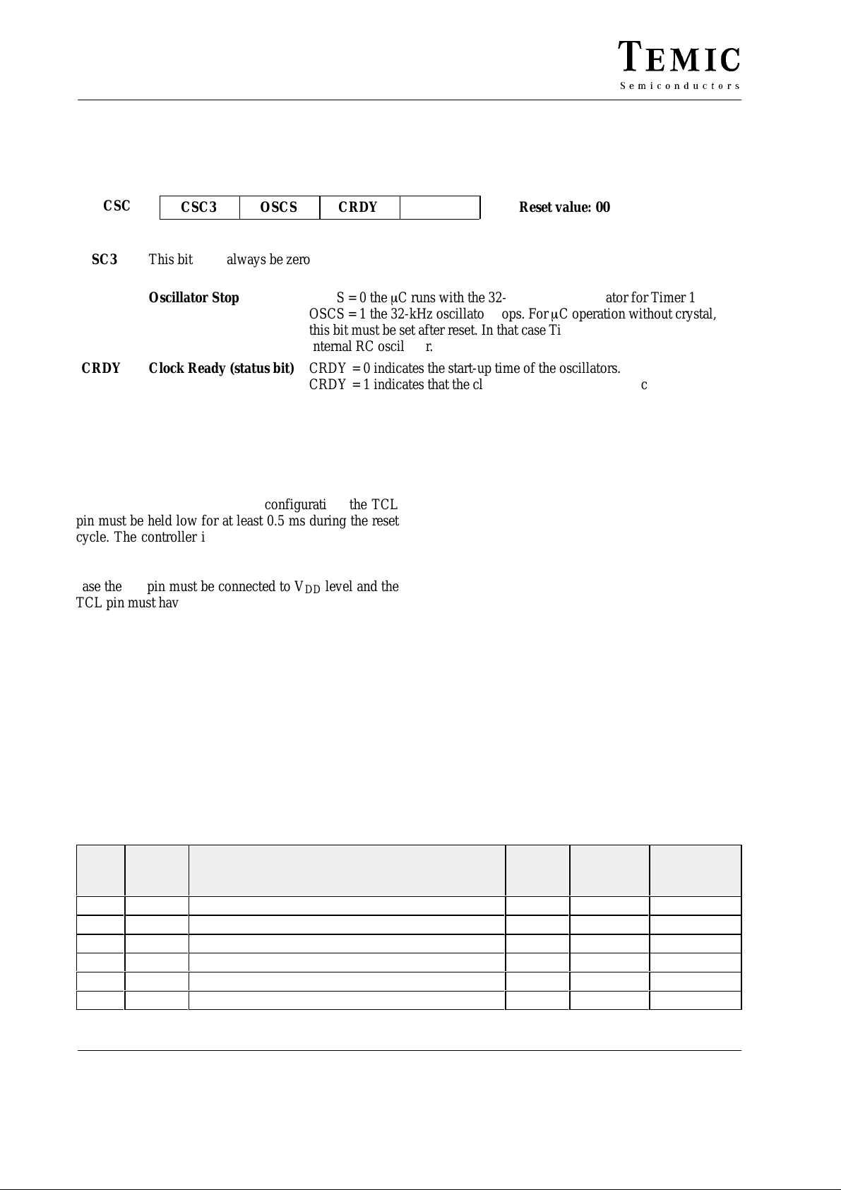
1.4.1 Clock Status/Control Register (CSC)
Bit 3 Bit 2 Bit 1 Bit 0
CSC
ÁÁÁ
CSC3
ÁÁÁ
OSCS
ÁÁ
CRDY
ÁÁÁ
CCS
ÁÁÁ
Address: Ch Subaddress: 2h
Reset value: 0000h
БББББББ
CSC3
ÁÁ
OSCS
ÁÁ
ÁÁ
CRDY
ÁÁ
CCS
This bit must always be zero
БББББББББББББББББББББББББББ
Oscillator Stop OSCS = 0 the mC runs with the 32-kHz crystal oscillator for Timer 1
БББББББББББББББББББББББББББ
БББББББББББББББББББББББББББ
OSCS = 1 the 32-kHz oscillator stops. For mC operation without crystal,
this bit must be set after reset. In that case Timer 1 is provided from the
internal RC oscillator.
Clock Ready (status bit) CRDY = 0 indicates the start-up time of the oscillators.
БББББББББББББББББББББББББББ
CRDY = 1 indicates that the clock is ready and has the exact timing.
Core Clock Select CCS = 0 selects 1 MHz system clock (SYSCL/TCL)
CCS = 1 selects 2 MHz system clock (SYSCL/TCL)
1.4.2 TCL Signal
The TCL pin can be used as input to supply the controller
with an external clock. For this configuration, the TCL
pin must be held low for at least 0.5 ms during the reset
cycle. The controller is working with clock frequencies
up to 2.5 MHz. It is also possible to use the TCL pin as
output to supply peripherals with the system clock. In this
case the TE pin must be connected to V
level and the
DD
TCL pin must have a high impedance load.
1.5 Power Down Modes
The sleep mode is a shutdown condition which is used to
reduce the average system power consumption in applications where the µC is not fully utilized. In this mode the
system clock is stopped. The sleep mode is entered with
the SLEEP instruction. This instruction sets the interrupt
enable bit (I) in the condition code register to enable all
interrupts and stops the core. During the sleep mode the
peripheral modules remain active and are able to generate
interrupts. The µC exits the sleep mode with any interrupt
or a reset.
Table 4. Power consumption at different power down modes
Mode CPU-
Core
1
SLEEP
2
SLEEP
3
SLEEP
4
SLEEP
5
6
RUN
RUN
T1R=0 AND TAR=0 AND TBR=0 AND EERDY=1
T1R=X, TAR=0 AND TBR=0 AND EERDY=1
T1R=1 OR TAR=1 OR TBR=1 OR EERDY=0
T1R=X, TAR=1 OR TBR=1 OR EERDY=0
T1R=X, T AR=X, TBR=X, EERDY=X
T1R=X, T AR=X, TBR=X, EERDY=X
TIMER 1 [T1R]
TIMER 2 [TAR, TBR]
EEPROM [EERDY]
The sleep mode can only be kept when none of the interrupt pending or active register bits are set. The application
of the $AUTOSLEEP routine ensures the correct function
of the sleep mode.
The total power consumption is directly proportional to
the active time of the µC. For a rough estimation of the
expected average system current consumption, the following formula should be used:
(VDD, f
I
total
I
depends on VDD and f
DD
Osc
) = I
+ (IDD * T
Sleep
Osc
.
active/Ttotal
)
Systemclock Generator Stop
The M44C260/M48C260 has different power down
modes. When the MARC4 core enters the sleep mode and
no on-chip peripheral needs a clock signal (SYSCL), the
system clock oscillator is stopped. Therefore the programmer should stop Timer 1 and Timer 2 during the
sleep mode if they are not required. If the 32-kHz oscillator is not used, it should be stopped. Under this condition,
the power consumption is extremely low (see following
table).
RC Osc. 32-kHz-
Osc.
Power-
Consumption
[OSCS]
STOP
STOP
RUN
RUN
RUN
RUN
STOP
RUN
STOP
RUN
STOP
RUN
< 1.0 µA
< 1.0 µA
< 1 mA
< 1 mA
< 3 mA
< 3 mA
Rev . A2, 01-Oct-9812 (51)
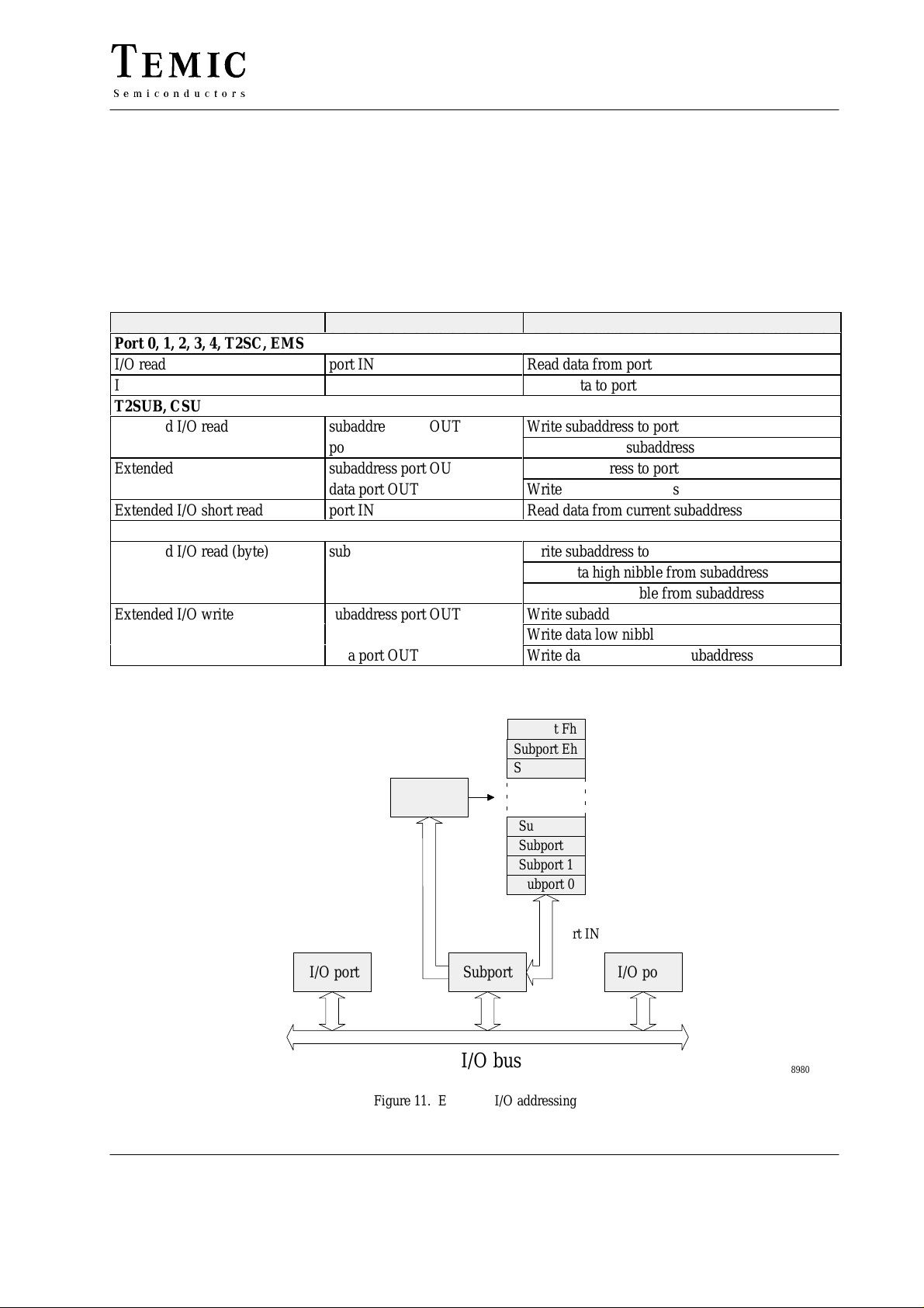
2 Peripheral Modules
2.1 Addressing Peripherals
The access to the peripheral modules (ports, registers) is
executed via the I/O bus. The IN- or OUT-instruction allows the direct addressing of 16 I/O ports. For peripherals
with a large number of registers, extended addressing is
used. With two I/O operations, an extended I/O port al-
Table 5. I/O-addressing
I/O Operation qFOR TH Instructions Description
Port 0, 1, 2, 3, 4, T2SC, EMS
I/O read
I/O write
T2SUB, CSUB
Extended I/O read
Extended I/O write
Extended I/O short read
ESUB
Extended I/O read (byte)
Extended I/O write (byte)
port IN
data port OUT
subaddress port OUT
port IN
subaddress port OUT
data port OUT
port IN
subaddress port OUT
port IN
port IN
subaddress port OUT
data port OUT
data port OUT
M44C260/M48C260
lows the access to 16 subports. The first OUT-instruction
writes the subport address to the subaddress register, the
second IN- or OUT-instruction reads data from or writes
data to the addressed subport.
Read data from port
Write data to port
Write subaddress to port
Read data from subaddress
Write subaddress to port
Write data to subaddress
Read data from current subaddress
Write subaddress to port
Read data high nibble from subaddress
Read data low nibble from subaddress
Write subaddress to port
Write data low nibble to subaddress
Write data high nibble to subaddress
Subport Fh
Subport Eh
Subport Dh
Subaddress
Register
Subport 3
Subport 2
subaddress port OUT
I/O port Subport I/O port
I/O bus
Figure 11. Extended I/O addressing
Rev . A2, 01-Oct-98 13 (51)
Subport 1
Subport 0
data port OUT
port IN
94 8980
M44C260/M48C260
Á
Á
Á
Á
Á
Á
Á
Á
Á
Á
Á
Á
Á
Á
Á
Á
Á
Á
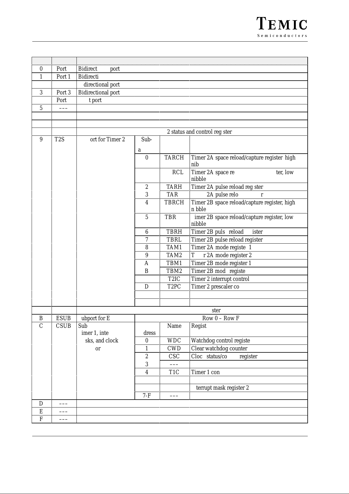
Table 6. Peripheral addresses
Addr. Name Function
0
Port 0
1
Port 1
2
Port 2
3
Port 3
4
Port 4
5
6
7
8
9
–––
–––
–––
T2SC
T2SUB
Bidirectional port
Bidirectional port
Bidirectional port
Bidirectional port
Input port
Subport for Timer 2
Timer 2 status and control register
Sub-
Name
Register
Á
ÁÁ
БББББ
address
ÁÁ
0
1
ÁÁÁÁÁБББББÁÁÁ
2
3
4
5
ÁÁÁÁÁБББББÁÁÁ
6
7
8
9
A
B
C
D
E
F
A
B
C
Á
EMS
ESUB
CSUB
ÁÁ
Subport for EEPROM
Subport for watchdog,
БББББ
Timer 1, interrupt
masks, and clock
generator
Sub-
ÁÁ
address
0
1
2
3
4
5
6
7-F
D
E
F
–––
–––
–––
ÁÁÁ
TARCH
ББББББББББББ
Timer 2A space reload/capture register , high
nibble
TARCL
ÁÁÁ
TARH
TARL
TBRCH
Timer 2A space reload/capture register , low
ББББББББББББ
nibble
Timer 2A pulse reload register
Timer 2A pulse reload register
Timer 2B space reload/capture register , high
nibble
TBRCL
ÁÁÁ
TBRH
TBRL
TAM1
TAM2
TBM1
TBM2
T2IC
T2PC
Timer 2B space reload/capture register , low
ББББББББББББ
nibble
Timer 2B pulse reload register
Timer 2B pulse reload register
Timer 2A mode register 1
Timer 2A mode register 2
Timer 2B mode register 1
Timer 2B mode register 2
Timer 2 interrupt control
Timer 2 prescaler control
–––
–––
EEPROM status register
Row 0 – Row F
Name
ÁÁÁ
WDC
CWD
CSC
Register
ББББББББББББ
Watchdog control register
Clear watchdog counter
Clock status/control register
–––
T1C
IMR1
IMR2
Timer 1 control register
Interrupt mask register 1
Interrupt mask register 2
–––
Rev . A2, 01-Oct-9814 (51)
M44C260/M48C260
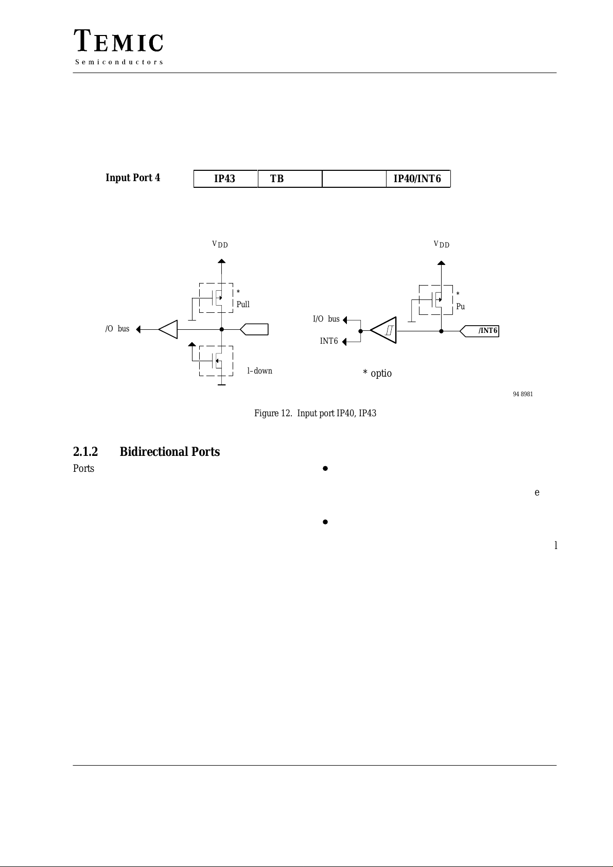
2.1.1 Input Port 4
Port 4 is the input port for the pins IP40, IP43, TA and TB. IP40 is also the interrupt input for INT6, and TA and TB
are normally used for timer I/O functions.
Bit 3 Bit 2 Bit 1 Bit 0
Input Port 4
IP43
TB/IP42
TA/IP41
IP40/INT6
V
DD
*
Pull–up
I/O bus
V
DD
IP43
*
Pull–down
Figure 12. Input port IP40, IP43
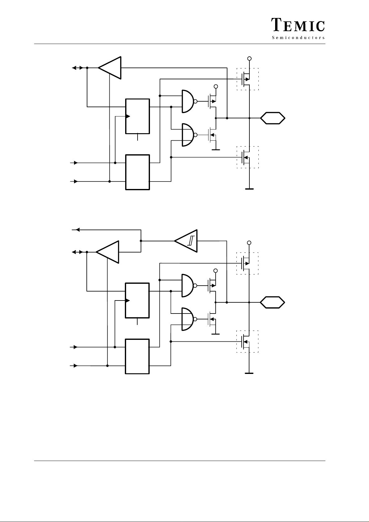
2.1.2 Bidirectional Ports
Ports 0, 1, 2 and 3 are bidirectional 4-bit wide ports and
may be used for data input or output. The data direction
is programmable for a complete port only. The port is
switched to output with an OUT-instruction and to input
with an IN-instruction. The data written to a port will be
stored into the output latches and appears immediately
after the OUT -instruction at the port pin. After RESET all
output latches are set to Fh and the ports are switched to
input mode.
Note: Care must be taken when switching bidirectional
ports from output to input. The capacitive load at
this port may cause the data read to be the same
as the last data written to this port. To avoid this
when switching the direction, one of the following approaches should be used.
V
DD
*
Pull–up
I/O bus
IP40/INT6
INT6
* optional
D
Use two IN-instructions and DROP the first data
nibble read. The first IN switches the port from output
to input, DROP removes the first invalid nibble and
the second IN reads the valid nibble.
D
Use an OUT-instruction followed by an IN-instruction. With the OUT-instruction, the capacitive load is
charged or discharged depending on the optional
pull-up /pull-down configuration. Write a “1” for pins
with pull-up resistors and a “0” for pins with pulldown resistors.
94 8981
Rev . A2, 01-Oct-98 15 (51)
M44C260/M48C260
I/O bus
D
R
Reset
OUT
IN
/ Reset
SQQ
R
NQ
Figure 13. Bidirectional port
V
DD
V
DD
*) optional
pull–up / pull–down
resistor
*
BPxy
*
94 8982
Interrupt logic
I/O bus
PortX_OUT
PortX_IN
/ Reset
(INT2 / INT3)
D
R
Reset
SQQ
*) optional
R
NQ
Figure 14. Bidirectional Port 3 with interrupt input
pull–up / pull–down
resistor
V
DD
*
V
DD
BP3y
*
94 8983
2.1.3 External Interrupt Inputs
The pins IP40 and BP30 – BP33 can be used as external
interrupt inputs. IP40 is used for INT6, BP32 and BP33
are used for INT3, and BP30 and BP31 are used for INT2.
Pin IP40 is also used as an input port and BP30 – BP33 as
a bidirectional port (see figure 14). Each of these external
interrupt sources can be enabled or disabled with individual interrupt mask bits. A negative transition at one of
these inputs requests an interrupt, when the corresponding mask bit is set. The interrupt masks are placed in the
subport registers IMR1 and IMR2 of port CSUB.
Rev . A2, 01-Oct-9816 (51)

M44C260/M48C260
IMR1:
IM32 IM31 IM30
IM33
BP33
BP32
BP31
BP30
IP40
IMR2:
IM6 IMT1
Figure 15. External interrupt inputs
2.2 Timer 1
Timer 1 is an interval timer for generating interrupts. Additionally , the Timer 1 can be used as watchdog timer . The
timer consists of a programmable 18 stage divider which
is supplied with a 32-kHz clock and a 3-bit counter for the
watchdog function (see figure 16). The time interval for
a Timer 1 interrupt (INT4) can be programmed with the
timer control register from 1 ms up to 8.0 s. The Timer 1
Interrupt
interface
Interrupt
interface
Interrupt
interface
INT3
INT2
INT6
94 8984
interrupt is maskable with the IMT1 bit.
The time interval for a watchdog reset can be pro-
grammed with the watchdog control register for 0.5, 2.0,
8.0 or 16.0 s. When the watchdog is active (WDR = 1) the
controller is reset with the overflow of the 3-bit watchdog
counter. The application software has to ensure that the
watchdog counter is reset by a write access to the CWD
port before it overflows.
T1C
T1R T1C1 T1C0
WRITE (T1C)
Divider
WDC
WDR
T1C2
CL32
DIVIDER
RESET
WDC1
WDC0
T1C2
0000
T1C1
0
T1C0
0
Decoder 3 : 8
Q5 Q6 Q8 Q10 Q12 Q14Q11 Q13 Q15 Q16 Q18
Decoder 2 : 4
1
0
1
0
WDC1
WDC0
1
1
1
0
0
0
0
1
0
0
1
Figure 16. Timer 1
1
11
01
1
1
1
0
11
IMT1=0
IMT1=1
IMR2
IM6
IMT1
Watchdog counter
WDR=0
WDR=1
Divider /8
Divider
RESET
WRITE CWD
INT4
RESET
(NRST)
94 8985
Rev . A2, 01-Oct-98 17 (51)

M44C260/M48C260
Á
Á
Á
Á
Á
Á
Timer 1 register
prescaler control register T1C. The interrupt mask IMT1
is placed in the interrupt mask register IMR2. The watchThe registers of Timer 1 are I/O-mapped. They are subport register of port CSUB the access is made by extended
I/O operations. The interval timer is controlled by the
dog timer is controlled by the watchdog control register
WDC and port CWD. A write access to CWD resets the
watchdog counter .
2.2.1 T1C – Timer 1 Control Register
Address: ‘C’h Subaddress 4
Bit 3 2 1 0
TIC
T1R
ÁÁ
T1C2
T1C1
T1C0
Timer 1 reset
БББББББББББББББББББББББББББ
Write (T1R = 1) resets the interval timer
Timer 1 control bit 2
Timer 1 control bit 1
Timer 1 control bit 0
This three bits select the time interval for a Timer 1 interrupt.
T1C2 T1C1 T1C0 Divider Time Interval
0
0
0
0
1
1
1
1
T1R
0
0
1
1
0
0
1
1
T1C2
0
1
0
1
0
1
0
1
T1C1
T1C0
32
64
256
1024
4096
16384
65536
262144
Reset value: 0000b
0.9765625 ms
1.953125 ms
7.8125 ms
31.25 ms
125 ms
500 ms
2 s
8 s
2.2.2 WDC – Watchdog Control Register
Bit 3 2 1 0
WDR
ÁÁ
ÁÁ
WDM1
WDM0
WDC
Watchdog run
БББББББББББББББББББББББББББ
WDR = 0 the watchdog counter is inactive and reset
БББББББББББББББББББББББББББ
WDR = 1 the watchdog counter is active and able to generate a reset when Timer 1 is running
Watchdog mode 1
Watchdog mode 0
Both these bits control the time interval for the watchdog reset.
WDR
–––
WDM1
WDM0
Address: ‘C’h Subaddress 0
Reset value: 0x00b
Rev . A2, 01-Oct-9818 (51)

M44C260/M48C260
WDM 1 WDM 0 Divider Delay Time to Reset (s)
0
0
1
1
2.3 Timer 2
Timer 2 consists of the two timer/counter blocks T imer A
and Timer B. Each block has one 8-bit downcounter and
a programmable prescaler. The clock inputs can be programmed to count the system clocks, Timer A clocks or
external clocks. The maximum clock rate for external
clocks is the half system clock frequency (SYSCL/2).
Each counter has a reload register for the pulse time and
a reload register for the space time. Every counter underflow toggles the output and reloads the downcounter
alternately from the pulse reload register or from the
space reload register. This allows the generation of any
duty cycles.
In addition, both counters have a capture mode. In this
mode an external signal or the Counter B output causes
the current counter value to be captured into the corresponding capture register .
The timer has two I/O pins, TA for Timer A and TB for
Timer B. Used as output, the pins have a high level during
the pulse time and a low level during the space time of the
timer. As input, the pins are used for the external counter
clock or the capture signal. The inputs have a programmable edge detection to select the active edge of an
external clock or capture signal.
Interrupts can be generated when a counter underflow or
a capture event occurs. The interrupt function for Timer
2 can be programmed with the interrupt control register.
Both counter blocks share one interrupt vector (INT5).
Timer 2 Modes
0
1
0
1
2048
8192
32768
524288
0.5
2
8
16
TA/TB pin is used as counter output. The duty cycle
can be programmed with the pulse and space reload
register.
D
Capture mode
Counter A/B is supplied by the system clock. The
TA/TB pin is used as input. An external signal at the
input causes the current counter value to be captured
into the capture register.
D
Event counter
Counter A/B counts external clocks at the TA/TB pin.
The capture register contains the current counter
value and can be read.
Combined Timer Modes
D
16-bit timer
Counter A is supplied with the system clock and its
output is coupled with the input of Counter B. In this
mode the counter is used to generate timer interrupts.
D
16 bit capture mode
Counter A is supplied with the system clock and
Counter B with the output of Counter A. An external
signal at the TA pin causes the current counter value
will be captured into the capture registers.
D
16-bit event counter
The output of Counter A is coupled with the input of
Counter B to count external clocks at T A. The capture
register of both counters contain the current counter
values.
D
There are various timer/counter modes for both blocks of
Timer 2. They can be used separately or combined. The
timer modes can be programmed with the timer control
and mode registers.
Single Timer Modes
D
8-bit timer
Counter A/B is supplied by the system clock and is
used to generate timer interrupts.
D
Pulse width modulation
Counter A/B is supplied by the system clock. The
Rev . A2, 01-Oct-98 19 (51)
Burst generator
Counter A is supplied with the system clock and its
output is coupled with the input of Counter B. The output of Counter B controls the output signal of Counter
A at the TA pin. The TA output is enabled during the
pulse and disabled during the space of Counter B.
D
Event counter with time gate
Counter A counts the clocks at the T A pin and Counter
B is supplied with the system clock. Each underflow
of Counter B causes the counter value of Counter A to
be captured into its capture register.

M44C260/M48C260
Timer 2 Register
All timer register are I/O mapped. The access to the
Timer 2 status control register (T2SC) can be done with
a direct I/O operation to T2SC. The status is read with an
IN operation and a command to control the timer is written with an OUT operation. The remaining registers of
SYSCL
Counter A
ACS
TAM1
ACE
TBM1
BCS1 BCS0
SYSCL
Counter B
BCE
Timer 2 are subport registers of port T2SUB. The access
to those registers needs an extended I/O operation. The
timer function can be configured with the mode registers
TAM1, TAM2, TBM1, TBM2 and the interrupt control
register T2IC. The timing depends on the contents of the
prescaler control register T2PC and the reload registers.
The capture registers are used to read the counter value.
TAM1
TARCH[r]
ACB
TAM2
TBM2
BCA
+
AGB
TAM2
AE1
AE0
INTERRUPT
T2IC
TAM1
AOE
TA
INT5
T2SC
[READ]
TBRCH[r]
Note: all control bit switches are shown at value “0”
Figure 17. Timer 2
Reload register
PULSE
T2PC
SPACE
TxRCH[w]TxRCL[w]TxRH[w] TxRL[w]
Input
Counter A/B
Prescaler
A/B
T2SC[w]
DOWN COUNTER A/B
Capture register
TxRCH[r] TxRCL[r]
TBM2
BE1
Toggle
x = A for Counter A,
B for Counter B
r = READ
w = WRITE
Capture
Input A/B
BE0
TB
BOE
TBM1
94 8987
Output
Counter A/B
94 8986
Figure 18. Counter A/B
Rev . A2, 01-Oct-9820 (51)

M44C260/M48C260
Á
Á
Á
Á
Á
Á
Á
Á
Á
Á
Á
Á
2.3.1 Timer 2 Status/Control Register (T2SC)
Control register Bit 3 2 1 0
Write (T2SC)
Status register
Read (T2SC)
TAM, T AR: Timer A control bits to start or stop Timer A.
TBM, TBR: Timer B control bits to start or stop T imer B.
TBM TAM TBR TAR Timer 2 Commands
1
1
0
0
0
0
0
0
1
0
0
1
1
0
0
0
0
1
x
x
0
1
0
1
0
1
x
TBM
TBSU
0
STOP_A
1
RUN_A
x
STOP_B
x
RUN_B
0
STOP_AB
1
RUN_AB
1
RUN_A-STOP_B
0
STOP_A-RUN_B
x
NOP
TAM
TBPC
TBR
TASU
A STOP command resets
the prescaler and counter.
A RUN command starts the
counter with the next clock
taking the value from the
pulse reload register.
TAR
TAPC
Address: 8
Reset value: 0000b
Reset value: 0000b
TBSU:
ÁÁ
ÁÁ
TBPC:
ÁÁ
Timer B end of space/underflow status bit.
БББББББББББББББББББББББББББ
When BCE* = 0 this bit will be set at the end of space time of Counter B.
БББББББББББББББББББББББББББ
When BCE = 1 this bit will be set with every Counter B underflow.
Timer B end of pulse/capture status bit.
When BCE = 0 this bit will be set at the end of pulse time of Counter B.
БББББББББББББББББББББББББББ
When BCE = 1 this bit will be set when a capture event for Counter B occurs.
TASU:
ÁÁ
ÁÁ
TAPC:
ÁÁ
Timer A end of space/underflow status bit.
БББББББББББББББББББББББББББ
When ACE* = 0 this bit will be set at the end of space time of Counter A.
БББББББББББББББББББББББББББ
When ACE = 1 this bit will be set with each Counter A underflow.
Timer A end of pulse/capture status bit.
When ACE = 0 this bit will be set at the end of pulse time of Counter A.
БББББББББББББББББББББББББББ
When ACE = 1 this bit will be set when a capture event for Counter A occurs.
*) ACE and BCE are the capture enable control bits in the timer mode registers TAM2 and TBM2.
The status bits TASU, T APC, TBSU, TBPC will be reset after a READ access to T2SC!
Rev . A2, 01-Oct-98 21 (51)

M44C260/M48C260
2.3.2 Timer 2 Subport (T2SUB)
Address: 9
Table 7. Timer 2 subports
Subaddr. Name Meaning Bit 3 Bit 2 Bit 1 Bit 0
0
1
2
3
4
5
6
7
8
9
A
B
C
D
E
F
T ARCH [w]*
TARCH [r]*
TARCL [w]*
TARCL [r]*
TARH
TARL
TBRCH [w]*
TBRCH [r]*
TBRCL [w]*
TBRCL [r]*
TBRH
TBRL
TAM1
TAM2
TBM1
TBM2
T2IC
T2PC
–––
–––
Timer A reload high
Timer A capture high
Timer A reload low
Timer A capture low
Timer A reload high
Timer A reload low
Timer B reload high
Timer B capture high
Timer B reload low
Timer B capture low
Timer B reload high
Timer B reload low
Timer A mode register 1
Timer A mode register 2
Timer B mode register 1
Timer B mode register 2
Timer 2 interrupt control
Timer 2 prescaler control
–––
ACB
–––
BCA
IMBS
BPC1
–––
–––
High-nibble
Low-nibble
High-nibble
Low-nibble
High-nibble
Low-nibble
High-nibble
Low-nibble
AGB
ACE
BCS1
BCE
IMBP
BPC0
–––
–––
ACS
AE1
BCS0
BE1
IMAS
APC1
–––
–––
AOE
AE0
BOE
BE0
IMAP
APC0
–––
–––
* [w] write only, [r] read only
2.3.3 Timer 2 Reload Register
The 8-bit wide reload registers of Timer A and B are used
to program the pulse and space width of the counter output signal.
The first clock after a start command loads the downcounter with the value (n) from the pulse reload register
and sets the counter output to 1. The downcounter decrements with each following clock and each underflow
reloads alternately the value (m) from the space reload
Prescaler out
Counter out
n n–1 n–2 1
n + 1 m + 1
PULSE
register or the value (n) from the pulse reload register and
toggles the counter output.
The pulse and space width can be calculated as following:
Pulse time: Pulse = (n+1) x prescaler clocks
Spacetime: Space = (m+1) x prescaler clocks
0 v m, n v 255
0
m m–1 m–2
SPACE
1
0
n
Rev . A2, 01-Oct-9822 (51)

M44C260/M48C260
Á
Á
Á
Á
Á
Á
Á
Á
Timer 2 Space Reload Register
The space reload register of Timer 2 is programmed by
two write accesses to the subport addresses TARCH and
TARCL or TBRCH and TBRCL of the Timer 2 subport
T2SUB. The value (m) in the space reload register determines the space width. At the end of the pulse, the
downcounter reloads the 8–bit value from the space reload register with the next clock of the prescaler output.
Space width: Space = (m+1) prescaler clocks
0 ≤ m ≤ 255
Timer 2 Pulse Reload Register
The pulse reload register of Timer 2 is programmed by
two write accesses to the subport addresses TERH and
TARL or TBRH and TBRL of the Timer 2 subport
T2SUB. The value (n) in the pulse reload register determines the space width. At the end of space the
downcounter reloads the 8-bit value from the pulse reload
register with the next clock of the prescaler output.
Pulse width: Pulse = (n+1) prescaler clocks
0 ≤ n ≤ 255
2.3.4 Timer 2 Capture Register
The capture register is used to capture the current downcounter value when a capture event occurs. The value is
kept in the capture register until the next capture event
and can be read independent of the state of the downcounter. The capture events are programmable with the
timer mode registers TAM2 and TBM2.
The capture registers are also used to read the counter
value when the external capture mode is disabled. In this
case the 8-bit counter value is transferred into the capture
register by reading the high nibble TARCH or TBRCH.
If the 16-bit event counter mode is enabled the complete
16-bit value is captured by reading first the high nibble
TARCH of Timer A. This mechanism ensures the coherence of the counter high and low nibble during the read
access.
2.3.5 Timer A Mode Register 1 (TAM1)
Bit 3 2 1 0
AGB
ÁÁ
ACS
ÁÁ
ÁÁ
AOE
ÁÁ
TAM1
Counter A output gated by Counter B output
AGB = 1 enables the burst generation mode. The output of Timer A is enabled during the pulse time
БББББББББББББББББББББББББББ
of the Counter B and disabled (TA= 0) during the space time of the Counter B.
Counter A clock select
БББББББББББББББББББББББББББ
This bit selects the source of the Counter A clock. When ACS = 0 the timer is supplied with internal
SYSCL. When ACS = 1 the timer is supplied with an external clock on TA pin.
БББББББББББББББББББББББББББ
Timer A output enable
AOE = 0 disables the counter output TA.
БББББББББББББББББББББББББББ
AOE = 1 enables the counter output TA.
–––
AGB
ACS
AOE
Address: 9 – Subaddress: 8
Reset value: 0000b
Rev . A2, 01-Oct-98 23 (51)

M44C260/M48C260
ÁÁÁ
БББББББББББББ
ÁÁÁ
БББББББББББББ
Á
Á
Á
Á
Á
Á
Á
Á
ББББББББББББББББББББББББББББ
ББББББББББББББББББББББББББББ
ББББББББББББББББББББББББББББ
Á
Á
ББББББББББББББББББББББББББББ
Á
Á
2.3.6 Timer A Mode Register 2 (TAM2)
Bit 3 2 1 0
TAM2
ACB
ACE
AE1
AE0
Address: 9 – Subaddress: 9
Reset Value: 0000b
ACB
ÁÁ
ÁÁ
ACE
ÁÁ
ÁÁ
AE1
AE0
Timer A captured by Timer B
Selects the capture source for Timer A. When ACB = 0 the signal at the TA pin is used to generate a
БББББББББББББББББББББББББББ
capture event. When ACB = 1 each transition at the Counter B output is used to generate a capture
БББББББББББББББББББББББББББ
event for Timer A.
Timer A capture enable
БББББББББББББББББББББББББББ
ACE = 1 enables the capture mode for Counter A. The occurrence of a capture event causes that the
current downcounter value is loaded into the capture register.
БББББББББББББББББББББББББББ
Timer A edge select bit 1
Timer A edge select bit 0
With these bits the active edge for the counter clocks and capture signal is selected.
AE1 AE0 Active Edge for Counter Clock/Capture Events
0
0
1
1
0
positive edge at TA pin
1
negative edge at TA pin
0
first positive edge after timer start and then each transition at TA pin
1
first negative edge after timer start and then each transition at TA pin
2.3.7 Timer B Mode Register 1 (TBM1)
Bit 3 2 1 0
TBM1
–––
BCS1
BCS0
BOE
Address: 9 – Subaddress: Ah
Reset value: 0000b
BCS1
BCS0
Timer B clock select bit 1
Timer B clock select bit 0
These bits select the source of Counter B clock.
BCS1 BCS0 Counter B Input Signal
0
1
x
BOE
ÁÁÁ
ÁÁÁ
0
System clock (SYSCL)
0
Output signal of Counter A
1
External input signal at TB
Timer B output enable
БББББББББББББББББББББББББББ
BOE = 0 disables the counter output TB.
БББББББББББББББББББББББББББ
BOE = 1 enables the counter output TB.
Rev . A2, 01-Oct-9824 (51)

2.3.8 Timer B Mode Register 2 (TBM2)
ÁÁÁÁ
ÁÁÁÁ
Á
Á
Á
Á
Á
Á
Á
Á
Á
Á
Bit 3 2 1 0
TBM2
BCA
BCE
BE1
M44C260/M48C260
Address: 9 – Subaddress: Bh
BE0
Reset value: 0000b
BCA
Timer B is captured with T imer A capture signal. With BCA = 1 the external capture signal for
Timer A is used to capture T imer B simultaneously with Timer A.
BCE
ÁÁ
ÁÁ
BE1
BE0
ÁÁ
Timer B capture enable
БББББББББББББББББББББББББББ
BCE = 1 enables the capture mode for Counter B. A capture event loads the current downcounter
БББББББББББББББББББББББББББ
value into the capture register.
Timer B edge select bit 1
Timer B edge select bit 0
With these bits the active edge for the counter clocks and capture signal is selected.
БББББББББББББББББББББББББББ
BE1 BE0 Active Edge for Clock/Capture Events
0
0
1
1
0
positive edge on TB pin
1
negative edge on TB pin
0
first positive edge after start timer and then each transition on TB pin
1
first negative edge after start timer and then each transition on TB pin
2.3.9 Timer 2 Prescaler Control Register (T2PC)
Bit 3 2 1 0
T2PC
BPC1
BPC0
APC1
APC0
Address: 9 – Subaddress: Dh
Reset Value: 0000b
BPC1
BPC0
ÁÁ
APC1
APC0
ÁÁ
Timer B prescaler control bit 1
Timer B prescaler control bit 0
БББББББББББББББББББББББББББ
These bits determine the divider for the prescaler of Timer B.
Timer A prescaler control bit 1
Timer A prescaler control bit 0
These bits determine the divider for the prescaler of Timer A.
БББББББББББББББББББББББББББ
BPC1/APC1 BPC0/APC0 Divider
0
0
1
1
0
1
0
1
1
4
16
64
Rev . A2, 01-Oct-98 25 (51)

M44C260/M48C260
Á
Á
Á
Á
Á
Á
Á
Á
Á
Á
Á
Á
2.3.10 Timer 2 Interrupt Control Register (T2IC)
Bit 3 2 1 0
T2IC
IMBS
IMBP
IMAS
IMAP
Address: 9 – Subaddress: Ch
Reset value: 0000b
IMBS
ÁÁ
IMBP
ÁÁ
ÁÁ
IMAS
ÁÁ
IMAP
ÁÁ
ÁÁ
Interrupt mask Timer B end of space/underflow
IMBS = 1 enables an INT5 interrupt, if BCE* = 0 at the end of space of Counter B,
БББББББББББББББББББББББББББ
or if BCE = 1 at each Counter B underflow.
Interrupt mask Timer B end of pulse/capture
БББББББББББББББББББББББББББ
IMBP = 1 enables an INT5 interrupt, if BCE = 0 at the end of pulse of Counter B,
or if BCE = 1 with a capture event for Counter B.
БББББББББББББББББББББББББББ
Interrupt mask Timer A end of space/underflow
IMAS = 1 enables an INT5 interrupt, if ACE* = 0 at the end of space of Counter A,
БББББББББББББББББББББББББББ
or if ACE = 1 at each Counter A underflow.
Interrupt mask Timer A end of pulse/capture
БББББББББББББББББББББББББББ
IMAP = 1 enables an INT5 interrupt, if ACE = 0 at the end of pulse of Counter A,
or if ACE = 1 with a capture event for Counter A.
БББББББББББББББББББББББББББ
Each interrupt source can be enabled or disabled individually by setting the corresponding maskbit.
*) ACE and BCE are the capture enable control bits in the timer mode registers TAM2 and TBM2.
T2SC[r] :
TBSU TBPC TASU
TAPC
Timer A end of
pulse / capture
Timer A end of
space / underflow
Timer B end of
pulse / capture
Timer B end of
space / underflow
T2IC :
IMBS IMBP IMAS IMAP
Figure 19. Timer 2 interrupt mask register
INT5
[r] = READ
94 8988
Rev . A2, 01-Oct-9826 (51)

2.3.11 Timer I/O (TA/TB)
The timer I/O pins TA and TB are used as input for the
external clock or capture signal and as output for the
counter. The mode is controlled with AOE and BOE
control bit. When AOE/BOE = 0 the pin is switched to
M44C260/M48C260
input mode, when AOE/BOE = 1 the pin is switched to
output mode. The pins also can be read with an INinstruction via Port 4 (TA with IP41 and TB with IP42).
I/O bus
(IP41/IP42)
Port4_IN
Counter input
(edge sense)
Counter output
AOE/AOB–controlbit
V
DD
*) optional
pull–up / pull–down
resistor
Figure 20. Timer I/O (TA/TB)
V
DD
*
TA/TB
*
94 8989
Rev . A2, 01-Oct-98 27 (51)

M44C260/M48C260
2.4 EEPROM
The EEPROM of the M44C260/M48C260 is 128 bit wide
and organized as an array of 16*8-bit. The EEPROM rows
are I/O mapped and are subports of port ESUB. The
Row
NWP
High nibble Low nibble
15
12
Memory
0
Control logic
access to any 8-bit row of the EEPROM is done by an
extended 8-bit I/O operation or by special postincrement
access. The EEPROM rows 12 to 15 can be write protected by hardware and software.
Write protectable
INT 1
EMS ESUB
Figure 21. EEPROM
2.4.1 EEPROM SubPort (ESUB)
Address: Bh – Subaddress: 0-Fh
Read operation
A read operation needs an OUT- and two IN-instructions
to port ESUB. First the OUT operation writes the row ad-
qFORTH example:
Row address ESUB OUT ( ––)
ESUB IN ( ––Data_High)
ESUB IN (Data_High –– Data_High Data_Low)
Write operation
A write operation needs three OUT-instructions to port
ESUB. The first operation writes the row address. The
following two OUT-instructions write the low nibble and
dress. The following two IN-instructions read the high
nibble and then the low nibble of the addressed row.
then the high nibble to the addressed row. After reset,
rows 12 to 15 are write protected. To enable write operations to these rows the write enable bit (EWE) must be set.
In all cases write accesses to these rows are disabled when
pin NWP is low.
94 8990
Rev . A2, 01-Oct-9828 (51)

M44C260/M48C260
Á
Á
Á
Á
Á
Á
Á
Á
Á
Á
qFORTH example:
Row address ESUB OUT (Data_High Data_Low –– Data_High Data_Low)
ESUB OUT (Data_High Data_Low ––Data_High)
ESUB OUT (Data_High ––)
The internal EEPROM write cycle needs about 16 ms
(with connected quartz crystal and running crystal oscillator). During this cycle the EEPROM ready bit is reset
(EPR = 0). After the data high nibble is written to the port
ESUB, the internal write cycle is started. During the
internal write cycle (while EPR = 0), only read and write
accesses to the EMS register are possible. All other
EEPROM accesses have no effect.
Postincrement operations
The postincrement mode supports a fast access to
consecutive EEPROM rows. A postincrement access is
started by setting the EPI bit in the EEPROM mode register (EMS) followed by writing the row start address to
port ESUB. After that, the read or write operations to the
consecutive EEPROM area, beginning at the start ad-
2.4.2 EEPROM Mode/Status Register (EMS)
Mode register Bit 3 2 1 0
Write (EMS)
Status register
Read (EMS)
–––
–––
EWE
–––
dress, need only two IN- or OUT-instructions to read or
write the data. The row address is incremented automatically after each complete row access (2 nibbles). A write
access to the EEPROM mode register (EMS) terminates
the postincrement mode.
Note: In the postincrement mode, it is not possible to
change from read to write operations or vice
versa before the current postincrement operation
is finished.
Write ready interrupt (INT1)
At the end of the internal write cycle an interrupt is generated when the interrupt mask bit IMEP in the EEPROM
mode register EMS is set. With this interrupt, successive
write operations can be executed interrupt controlled
within the INT1 interrupt service routine.
Address: Ah
EPI
–––
IMEP
EPR
Reset value: 0000b
Reset value: xxx1b
EWE
ÁÁ
EEPROM write enable bit
EWE = 0 disables write accesses to rows 12-15
БББББББББББББББББББББББББББ
EWE = 1 enables write accesses to rows 12-15 when the NWP pin is high
EPI
ÁÁ
IMEP
ÁÁ
EPR
ÁÁ
ÁÁ
EEPROM postincrement mode enable
БББББББББББББББББББББББББББ
EPI = 1 activates a postincrement access after the next row address is written to port ESUB
Interrupt mask for EEPROM write ready interrupt
БББББББББББББББББББББББББББ
When IMEP is set an INT1 is generated with the end of the internal EEPROM write cycle
EEPROM ready status flag
EPR = 0 indicates that the EEPROM is not ready for read or write operations
БББББББББББББББББББББББББББ
(an internal write cycle is executed)
БББББББББББББББББББББББББББ
EPR = 1 indicates that the EEPROM is ready for read and write operations
After a write access to the EMS-Register, postincrement operations are terminated and any incomplete EEPROM read
and write sequence must be started again!
Rev . A2, 01-Oct-98 29 (51)

M44C260/M48C260
3 Appendix
3.1 Emulation
For emulation all MARC4 controllers have a special
emulation mode. It is activated by setting the TE pin to
logic HIGH level during reset. In this mode the internal
CPU core is inactive and the I/O buses are available via
Port 0 and Port 1 to allow the emulator the access to the
on-chip peripherals. The emulator contains a special
emulation CPU with a MARC4 core and additional breakpoint logic and takes over the core function. The basic
function of the emulator is to evaluate the customer’s program and hardware in real time. Thus, the analysation of
any timing, hardware or software problems the simulation of the application is possible. For more information
about emulation see “Emulator Manual”.
3.2 Programming the EEPROM
Program Memory
Programming the 4K 8-bit EEPROM program memory
is done using a special PC-controlled programming device. Details on how to use this device and the
corresponding software are given in the Programming
Device User Manual.
To start programming the data memory, the microcontroller is switched to a special I/O mode, where the
core and all peripherals are set inactive and the two I/O
buses are available via Port 0 (data) and Port 1 (control).
Then the customer application data is transfered to the
controller via Port 0 in blocks of 64 nibble size. Programming is started automatically after each block. The
programming high voltage is generated on chip.
After programming the memory, a verify run is started
where the just written data is read out and compared bit
by bit to the original source file. This ensures that the content of the ROM is error free.
3.3 MARC4 Instruction Set
The MARC4 instruction set is optimized for the high level
programming language qFORTH. A lot of MARC4
instructions are qFORTH words. This enables the compiler to generate a fast and compact program code. The
MARC4 is a zero address machine with a compact and efficient instruction code. Most of the instructions are
single byte instructions. These operations are performed
and no source or destination address information . Only
BRANCH, CALL and RAM access instructions need address information and a length of two bytes for long
address operations. In total, there are five types of instruction formats with a length of one and two bytes.
Zero address operations such as arithmetical, logical,
shift and rotate operations are performed with data placed
on the top of the expression stack (TOS and TOS–1). Also
I/O– and stack operations are single byte zero address operations and are performed with the top expression stack
location.
A literal is a 4-bit constant value which is placed on the
data stack. In the MARC4 native code they are represented as LIT_<value>, where <value> is the
hexadecimal representation from 0 to 15 (0...F). This
range is a result of the MARC4’s 4-bit data width. The
6-bit short address and the 12-bit long address formats are
both used to address the byte-wide ROM via CALL and
conditional branch instructions. This results in a ROM
address space of up to 4K 8-bit words.
The MARC4 instruction includes both short and long call
instructions as well as conditional branch instructions. On
execution the address part of the instruction’s word is directly loaded into the program counter. Long call and
branch instructions can jump anywhere within the program memory area. The lower six bits from the short call
(SCALL) and short branch (SBRA) instruction are handled in a different way. The six bit SCALL address is
multiplied by three and then loaded into the PC. This
allows calls within the zero page (000 to 1FFh). The six
bit SBRA address is loaded immediately into the lower
six bits of the PC. This allows jumps within the 64 byte
segment addressed by the upper six bits of the PC.
The CALL and SCALL instructions write the incremented program counter contents to the return stack. This
address is loaded back to the PC when the associated
EXIT or RTI instruction is encountered. The long RAM
address format is used by the four 8-bit RAM address
registers which can be pre-increment, post-decrement or
loaded directly from the MARC4’s internal bus. This
results in a direct accessible RAM address space of up to
256 4-bit.
Rev . A2, 01-Oct-9830 (51)

M44C260/M48C260
Á
Á
Á
1) Zero address operation
(ADD,SUB, INC, OR,...)
2) Immediate data operation
Literal (LIT_0, LIT_1, ...)
3) Short ROM address operation
(SCALL, SBRA)
4) Long ROM address operation
(CALL, BRA)
5) RAM address operation
(>SP, >X,...)
7654
Opcode 4 bit data
7654
Opcode
Opcode
7654 3210 32107654
Figure 22. MARC4 opcode formats
3.3.1 MARC4 Instruction Set Overview
Mnemonic Description Cycles/
Bytes
Arithmetic operations:
ADD
ADDC
SUB
SUBB
DAA
INC
DEC
DECR
ÁÁÁ
CMP_EQ
CMP_NE
CMP_LT
CMP_LE
CMP_GT
CMP_GE
XOR
AND
OR
NOT
SHL
SHR
ROL
ROR
Add
Add with carry
Subtract
Subtract with borrow
Decimal adjust
Increment TOS
Decrement TOS
Decrement. 4-bit index on
БББББББ
return stack
Compare operations:
Compare equal
Compare not equal
Compare less than
Compare less equal
Compare greater than
Compare greater equal
Logical operations:
Exclusive OR
AND
OR
1’s complement
Shift left into carry
Shift right into carry
Rotate left through carry
Rotate right through carry
1/1
1/1
1/1
1/1
1/1
1/1
1/1
2/1
Á
1/1
1/1
1/1
1/1
1/1
1/1
1/1
1/1
1/1
1/1
1/1
1/1
1/1
1/1
Opcode
3210
3210
6 bit address
32105476
12 bit address11 0
Opcode 8 bit address
32107654 32107654
Mnemonic Description Cycles/
Flag operations:
TOG_BF
SET_BFC
DI
CCR!
CCR@
T oggle branch flag
Set branch flag
Disable all interrupts
Store TOS into CCR
Fetch CCR onto TOS
Program branching:
BRA $xxx
CALL $xxx
SBRA $xxx
SCALL$xxx
EXIT
RTI
SWI
SLEEP
NOP
Conditional long branch
Long call (current page)
Conditional short branch
Short call (zero page)
Return from subroutine
Return from interrupt
Software interrupt
Activate sleep mode
No operation
Register operations:
SP@
RP@
X@
Y@
SP!
RP!
X!
Y!
>SP $xx
>RP $xx
>X $xx
>Y $xx
Fetch the current SP
Fetch the current RP
Fetch the contents of X
Fetch the contents of Y
Move the top 2 into SP
Move the top 2 into RP
Move the top 2 into X
Move the top 2 into Y
Store direct address to SP
Store direct address to RP
Store direct address into X
Store direct address into Y
94 8708
Bytes
1/1
1/1
1/1
1/1
1/1
2/2
3/2
2/1
2/1
2/1
2/1
1/1
1/1
1/1
2/1
2/1
2/1
2/1
2/1
2/1
2/1
2/1
2/2
2/2
2/2
2/2
Rev . A2, 01-Oct-98 31 (51)

M44C260/M48C260
Á
Á
Á
Á
Á
Á
Á
Á
Á
Á
Á
Á
Á
Á
Á
Á
Á
Á
Á
Á
Á
Á
Á
Á
Á
Á
Á
Á
Á
Á
Á
Á
Á
Á
Á
Á
Á
Á
Á
Á
Á
Á
Á
Á
Á
Á
Á
Á
Mnemonic Description Cycles/
Bytes
Stack operations:
SWAP
OVER
DUP
ROT
DROP
>R
ÁÁÁ
2>R
Exchange the top 2 nibble
Copy TOS-1 to the top
Duplicate the top nibble
Move TOS-2 to the top
Remove the top nibble
Move the top nibble onto
the return stack
БББББББ
Move the top 2 nibble
1/1
1/1
1/1
3/1
1/1
1/1
Á
3/1
onto the return stack
3>R
ÁÁÁ
R@
Move the top 3 nibble
БББББББ
onto the return stack
Copy 1 nibble from the re-
4/1
Á
1/1
turn stack
2R@
ÁÁÁ
3R@
ÁÁÁ
DROPR
Copy 2 nibbles from the
БББББББ
return stack
Copy 3 nibbles from the
return stack
БББББББ
Remove the top of return
2/1
Á
4/1
Á
1/1
stack (12-Bit)
LIT_n
ÁÁÁ
Push immediate value
БББББББ
1/1
Á
(1 nibble) onto TOS
ROM data operations:
TABLE
ÁÁÁ
Fetch 8-bit constant from
БББББББ
ROM
Á
Mnemonic Description Cycles/
Bytes
Memory operations:
[X]@
[Y]@
ÁÁÁ
[+X]@
ÁÁÁ
[+Y]@
[X-]@
ÁÁÁ
[Y-]@
ÁÁÁ
[>X]@ $xx
[>Y]@ $xx
ÁÁÁ
[X]!
ÁÁÁ
[Y]!
[+X]!
ÁÁÁ
[+Y]!
[X-]!
ÁÁÁ
[Y-]!
ÁÁÁ
[>X]! $xx
ÁÁÁ
[>Y]! $xx
3
IN
OUT
Fetch 1 nibble from RAM
indirect addressed by X-
ББББББ
or Y-register
Fetch 1 nibble from RAM
indirect addr. by pre-in-
ББББББ
crem. X- or Y-register
Fetch 1 nibble from RAM
ББББББ
indirect addr. by post-dejcrem. X- or Y-register
ББББББ
Fetch 1 nibble from RAM
direct addressed by X- or
ББББББ
Y-register
Store 1 nibble into RAM
indirect addressed by [X]
ББББББ
Store 1 nibble into RAM
indirect addressed by pre-
ББББББ
incremented [X]
Store 1 nibble into RAM
ББББББ
indirect addr. by post-de-
ББББББ
crem. X- or Y-register
Store 1 nibble into RAM
direct addressed by X- or
ББББББ
Y-register
I/O operations:
Read I/O-Port onto TOS
Write TOS to I/O port
1/1
ÁÁ
1/1
ÁÁ
1/1
ÁÁ
ÁÁ
2/2
ÁÁ
1/1
ÁÁ
1/1
ÁÁ
1/1
ÁÁ
ÁÁ
2/2
ÁÁ
1/1
1/1
3.3.2 qFORTH Language Overview
MARC4 controllers are programmed in the high level
language qFOR TH which is based on the FORTH-83 language standard. The qFORTH compiler generates a
native code for a 4-bit FORTH-architecture single chip
microcomputer, the TEMIC MARC4.MARC4 applica-
tions are all programmed in qFORTH which is designed
specifically for efficient real time control. Since the
qFORTH compiler generates highly optimized codes,
there is no advantage or point in programming the
MARC4 in assembly code. The high level of code
efficiency generated by the qFORTH compiler is
achieved by the use of modern optimization techniques
such as branch-instruction size minimization, fast
procedure calls, pointer tracking and many peephole optimizations.
Language features:
Expandability
Many of the fundamental qFORTH operations
are directly implemented in the MARC4 instruction set.
Stack oriented
All operations communicate with one another
via the data stack and use the reverse polish form
of notation (RPN)
Structured programming
qFOR TH supports structured programming
Reentrant
Different tasks can share the same code.
Recursive
qFOR TH routines can call themselves.
Native code inclusion
In qFORTH there is no separation of high level
constructs from the native code mnemonics.
Rev . A2, 01-Oct-9832 (51)

M44C260/M48C260
3.4 The qFORTH Language - Quick Reference Guide
3.4.1 Arithmetic/Logical
- EXP ( n1 n2 –– n1-n2 ) Subtract the top two nibbles
+ EXP ( n1 n2 –– n1+n2 ) Add up the two top 4-bit values
-C EXP ( n1 n2 –– n1+/n+/C ) 1’s compl. subtract with borrow
+C EXP ( n1 n2 –– n1+n2+C ) Add with carry top two values
1+ EXP ( n –– n+1 ) Increment the top value by 1
1- EXP ( n –– n–1 ) Decrement the top value by 1
2* EXP ( n –– n*2 ) Multiply the top value by 2
2/ EXP ( n –– n DIV 2 ) Divide the 4-bit top value by 2
D+ EXP ( d1 d2 –– d1+d2 ) Add the top two 8-bit values
D- EXP ( d1 d2 –– d1-d2 ) Subtract the top two 8-bit values
D2/ EXP ( d –– d/2 ) Divide the top 8-bit value by 2
D2* EXP ( d –– d*2 ) Multiply the top 8-bit value by 2
M+ EXP ( d1 n –– d2 ) Add a 4-bit to an 8-bit value
M- EXP ( d1 n –– d2 ) Subtract 4-bit from an 8-bit value
AND EXP ( n1 n2 –– n1^n2 ) Bitwise AND of top two values
OR EXP ( n1 n2 –– n1 v n2 ) Bitwise OR the top two values
ROL EXP ( –– ) Rotate TOS left through carry
ROR EXP ( –– ) Rotate TOS right through carry
SHL EXP ( n –– n*2 ) Shift TOS value left into carry
SHR EXP ( n –– n/2 ) Shift TOS value right into carry
NEGATE EXP ( n –– –n ) 2’s complement the TOS value
DNEGATE EXP ( d –– –d ) 2’s complement top 8-bit value
NOT EXP ( n –– /n ) 1’s complement of the top value
XOR EXP ( n1 n2 –– n3 ) Bitwise Ex-OR the top 2 values
3.4.2 Comparisons
> EXP ( n1 n2 –– ) If n1>n2, then branch flag set
< EXP ( n1 n2 –– ) If n1<n2, then branch flag set
>= EXP ( n1 n2 –– ) If n1>=n2, then branch flag set
<= EXP ( n1 n2 –– ) If n1<=n2, then branch flag set
<> EXP ( n1 n2 –– ) If n1<>n2, then branch flag set
= EXP ( n1 n2 –– ) If n1=n2, then branch flag set
0<> EXP ( n –– ) If n <>0, then branch flag set
0= EXP ( n –– ) If n = 0, then branch flag set
D> EXP ( d1 d2 –– ) If d1>d2, then branch flag set
D< EXP ( d1 d2 –– ) If d1<d2, then branch flag set
D>= EXP ( d1 d2 –– ) If d1>=d2, then branch flag set
D<= EXP ( d1 d2 –– ) If d1<=d2, then branch flag set
D= EXP ( d1 d2 –– ) If d1=d2, then branch flag set
D<> EXP ( d1 d2 –– ) If d1<>d2, then branch flag set
D0<> EXP ( d –– ) If d <>0, then branch flag set
D0= EXP ( d –– ) If d =0, then branch flag set
DMAX EXP ( d1 d2 –– dMax ) 8-bit maximum value of d1, d2
DMIN EXP ( d1 d2 –– dMin ) 8-bit minimum value of d1, d2
MAX EXP ( n1 n2 –– nMax ) 4-bit maximum value of n1, n2
MIN EXP ( n1 n2 –– nMin ) 4-bit minimum value of n1, n2
Rev . A2, 01-Oct-98 33 (51)

M44C260/M48C260
3.4.3 Control Structures
AGAIN EXP ( –– ) Ends an infinite loop BEGIN .. AGAIN
BEGIN EXP ( –– ) BEGIN of most control structures
CASE EXP ( n –– n ) Begin of CASE .. ENDCASE block
DO EXP ( limit start –– ) Initializes an iterative DO..LOOP
RET ( –– u|limit|start )
ELSE EXP ( –– ) Executed when IF condition is false
ENDCASE EXP ( n –– ) End of CASE..ENDCASE block
ENDOF EXP ( n –– n ) End of <n> OF .. ENDOF block
EXECUTE EXP ( ROMAddr –– ) Execute word located at ROMAddr
EXIT RET ( ROMAddr –– ) Unstructured EXIT from ‘:’-definition
IF EXP ( –– ) Conditional IF .. ELSE .. THEN block
LOOP EXP ( –– ) Repeat LOOP, if index+1<limit
<n> OF EXP ( c n –– ) Execute CASE block, if n =c
REPEAT EXP ( –– ) Unconditional branch to BEGIN of BEGIN .. WHILE
REPEAT
THEN EXP ( –– ) Closes an IF statement
UNTIL EXP ( –– ) Branch to BEGIN, if condition is false
WHILE EXP ( –– ) Execute WHILE .. REPEAT block,
if condition is true
+LOOP EXP ( n –– ) Repeat LOOP, if I+n < limit
RET ( u|limit|I –– u|limit|I+n )
#DO EXP ( n –– ) RET ( –– u|u|n ) Execute the #DO .. #LOOP block n-times
#LOOP EXP ( –– ) Decrement loop index by 1 downto zero
RET ( u|u|I––u|u|I–1 )
?DO EXP ( Limit Start –– ) if start=limit, skip LOOP block
?LEAVE EXP ( –– ) Exit any loop, if condition is true
–?LEAVE EXP ( –– ) Exit any loop, if condition is false
3.4.4 Stack Operations
0 .. Fh, EXP ( –– n )
0 .. 15 EXP ( –– n ) Push 4-bit literal on EXP stack
’ <name> EXP ( –– ROMAddr ) Places ROM address
of colon-definition <name> on EXP stack
<ROT EXP ( n1 n2 n –– n n1 n2) Move top value to 3rd stack pos.
>R EXP ( n –– ) RET ( –– u|u|n ) Move top value onto the return stack
?DUP EXP ( n –– n n ) Duplicate top value, if n <>0
DEPTH EXP ( –– n ) Get current expression stack depth
DROP EXP ( n –– ) Remove the top 4-bit value
DUP EXP ( n –– n n ) Duplicate the top 4-bit value
I EXP ( –– I ) RET ( u|u|I — u|u|I ) Copy loop index I from return to expression stack
J EXP ( –– J ) Fetch index value of outer loop
[2nd return stack level
RET ( u|u|J u|u|I –– u|u|J u|u|I ) entry]
NIP EXP ( n1 n2 –– n2 ) Drop second to top 4-bit value
OVER EXP ( n1 n2 –– n1 n2 n1 ) Copy 2nd over top 4-bit value
PICK EXP ( × –– n[x] ) Copy the x-th value from the expression stack
onto TOS
RFREE EXP ( –– n ) Get # of unused RET stack entries
R> EXP ( –– n ) RET ( u|u|n –– ) Move top 4-bits from return to expression stack
R@ EXP ( –– n ) Copy top 4-bits from return to expression stack
RET ( u|u|n –– u|u|n )
ROLL EXP ( n –– ) Move n-th value within stack to top
Rev . A2, 01-Oct-9834 (51)

M44C260/M48C260
ROT EXP ( n1 n2 n –– n2 n n1) Move 3rd stack value to top pos.
SWAP EXP ( n1 n2 –– n2 n1 ) Exchange top two values on stack
TUCK EXP ( n1 n2 –– n2 n1 n2 ) Duplicate top value, move under second item
2>R EXP ( n1 n2 –– ) Move top two values from expression
to return stack
RET ( –– u|n2|n1 )
2DROP EXP ( n1 n2 –– ) Drop top 2 values from the stack
2DUP EXP ( d –– d d ) Duplicate top 8-bit value
2NIP EXP ( d1 d2 –– d2 ) Drop 2nd 8-bit value from stack
2OVER EXP ( d1 d2 –– d1 d2 d1 ) Copy 2nd 8-bit value over top value
2<ROT EXP ( d1 d2 d –– d d1 d2) Move top 8-bit value to 3rd pos’n
2R> EXP ( –– n1 n2 ) Move top 8-bits from return to expression stack
RET ( u|n2|n1 –– )
2R@ EXP ( –– n1 n2 ) Copy top 8-bits from return to expression stack
RET ( u|n2|n1 –– u|n2|n1)
2ROT EXP ( d1 d2 d –– d2 d d1) Move 3rd 8-bit value to top value
2SWAP EXP ( d1 d2 –– d2 d1 ) Exchange top two 8-bit values
2TUCK EXP ( d1 d2 –– d2 d1 d2 ) Tuck top 8-bits under 2nd byte
3>R EXP ( n1 n2 n3 –– ) Move top 3 nibbles from the expression onto
RET ( –– n3|n2|n1 ) the return stack
3DROP EXP ( n1 n2 n3 –– ) Remove top 3 nibbles from stack
3DUP EXP ( t –– t t ) Duplicate top 12-bit value
3R> EXP ( –– n1 n2 n3 ) Move top 3 nibbles from return
to the expression stack
RET ( n3|n2|n1 –– )
3R@ EXP ( –– n1 n2 n3 ) Copy 3 nibbles (1 entry) from the return
RET ( n3|n2|n1 –– n3|n2|n1 ) to the expression stack
3.4.5 Memory Operations
! EXP ( n addr –– ) Store a 4-bit value in RAM
@ EXP ( addr –– n ) Fetch a 4-bit value from RAM
+! EXP ( n addr –– ) Add 4-bit value to RAM contents
1+! EXP ( addr –– ) Increment a 4-bit value in RAM
1–! EXP ( addr –– ) Decrement a 4-bit value in RAM
2! EXP ( d addr –– ) Store an 8-bit value in RAM
2@ EXP ( addr –– d ) Fetch an 8-bit value from RAM
D+! EXP ( d addr –– ) Add 8-bit value to byte in RAM
D–! EXP ( d addr –– ) Subtract 8-bit value from a byte in RAM
DTABLE@ EXP ( ROMAddr n –– d ) Indexed fetch of a ROM constant
DTOGGLE EXP ( d addr –– ) Exclusive-OR 8-bit value with byte in RAM
ERASE EXP ( addr n –– ) Sets n memory cells to 0
FILL EXP ( addr n n1 –– ) Fill n memory cells with n1
MOVE EXP ( n from to –– ) Move a n-digit array in memory
ROMByte@ EXP ( ROMAddr –– d ) Fetch an 8-bit ROM constant
TOGGLE EXP ( n addr –– ) Ex-OR value at address with n
3! EXP ( nh nm nl addr –– ) Store 12-bit value into a RAM array
3@ EXP ( addr –– nh nm nl ) Fetch 12-bit value from RAM
T+! EXP ( nh nm nl addr –– ) Add 12-bits to 3 RAM cells
T–! EXP ( nh nm nl addr –– ) Subtract 12-bits from 3 nibble RAM array
TD+! EXP ( d addr –– ) Add byte to a 3 nibble RAM array
TD–! EXP ( d addr –– ) Subtract byte from 3 nibble array
Rev . A2, 01-Oct-98 35 (51)

M44C260/M48C260
3.4.6 Predefined Structures
( ccccccc) In-line comment definition
\ ccccccc Comment until end of the line
: <name> RET ( –– ) Begin of a colon definition
; RET ( ROMAddr –– ) Exit; ends any colon definition
[FIRST] EXP ( –– 0 ) Index (=0) for first array element
[LAST] EXP ( –– n|d ) Index for last array element
CODE EXP ( –– ) Begins an in-line macro definition
END-CODE EXP ( –– ) Ends an In-line macro definition
ARRAY EXP ( n –– ) Allocates space for a 4-bit array
2ARRAY EXP ( n –– ) Allocates space for an 8-bit array
CONSTANT EXP ( n –– ) Defines a 4-bit constant
2CONSTANT EXP ( d –– ) Defines an 8-bit constant
LARRAY EXP ( d –– ) Allocates space for a long 4-bit array
with up to 255 elements
2LARRAY EXP ( d –– ) Allocates space for a long byte array
Index EXP (n|d addr––addr’) Run-time array access using a variable array index
ROMCONST EXP ( –– ) Define ROM look-up table with 8-bit values
VARIABLE EXP ( –– ) Allocates memory for 4-bit value
2VARIABLE EXP ( –– ) Creates an 8-bit variable
<n> ALLOT Allocate space for <n+1> nibbles
of un-initialized RAM
A T <address> Fixed <address> placement
: INTx RET ( –– ROMAddr ) Interrupt service routine entry
: $AutoSleep Entry point address on return stack underflow
: $RESET EXP ( –– ) Entry point on power-on reset
3.4.7 Assembler Mnemonics
ADD EXP ( n1 n2 –– n1+n2 ) Add the top two 4-bit values
ADDC EXP ( n1 n2 –– n1+n2+C ) Add with carry top two values
CCR! EXP ( n –– ) Write top value into the CCR
CCR@ EXP ( –– n ) Fetch the CCR onto top of stack
CMP_EQ EXP ( n1 n2 –– n1 ) If n1=n2, then branch flag set
CMP_GE EXP ( n1 n2 –– n1 ) If n1>=n2, then branch flag set
CMP_GT EXP ( n1 n2 –– n1 ) If n1>n2, then branch flag set
CMP_LE EXP ( n1 n2 –– n1 ) If n1<=n2, then branch flag set
CMP_LT EXP ( n1 n2 –– n1 ) If n1<n2, then branch flag set
CMP_NE EXP ( n1 n2 –– n1 ) If n1<>n2, then branch flag set
CLR_BCF EXP ( –– ) Clear branch and carry flag
SET_BCF EXP ( –– ) Set branch and carry flag
TOG_BF EXP ( –– ) Toggle the branch flag
DAA EXP ( n>9 or C set –– n+6) BCD arithmetic adjust [addition]
DAS EXP ( n –– 10+/n+C ) 9’s complement for BCD subtract
DEC EXP ( n –– n–1 ) Decrement top value by 1
DECR RET ( u|u|I — u|u|I–1 ) Decrement value on the return stack
DI EXP ( –– ) Disable interrupts
DROPR RET ( u|u|u –– ) Drop element from return stack
EXIT RET ( ROMAddr –– ) Exit from current ‘:’-definition
EI EXP ( –– ) Enable interrupts
IN EXP ( port –– data ) Read data from an I/O port
INC EXP ( n –– n+1 ) Increment the top value by 1
NOP EXP ( –– ) No operation
NOT EXP ( n –– /n ) 1’s complement of the top value
Rev . A2, 01-Oct-9836 (51)

M44C260/M48C260
RP! EXP ( d –– ) Store as return stack pointer
RP@ EXP ( –– d ) Fetch current RET stack pointer
RTI RET ( RETAddr –– ) Return from interrupt routine
SLEEP EXP ( –– ) Enter ’sleep-mode’, enable all interrupts
SWI0 SWI7 EXP ( –– ) Software triggered interrupt
SP! EXP ( d –– ) Store as stack pointer
SP@ EXP ( –– d ) Fetch current stack pointer
SUB EXP ( n1 n2 –– n1-n2 ) 2’s complement subtraction
SUBB EXP ( n1 n2 –– n1+/n2+C ) 1’s compl. subtract with borrow
TABLE EXP ( –– d )
RET ( RetAddr RomAddr ––) Fetches an 8-bit constant from an address in ROM
OUT EXP ( data port –– ) Write data to I/O port
X@ EXP ( –– d ) Fetch current ×register contents
[X]@ EXP ( –– n ) Indirect × fetch of RAM contents
[+X]@ EXP ( –– n ) Pre-incr. × indirect RAM fetch
[X–]@ EXP ( –– n ) Postdecr. × indirect RAM fetch
[>X]@ $xx EXP ( –– n ) Direct RAM fetch, × addressed
X! EXP ( d –– ) Move 8-bit address to × register
[X]! EXP ( n –– ) Indirect × store of RAM contents
[+X]! EXP ( n –– ) Pre-incr. × indirect RAM store
[X–]! EXP ( n –– ) Postdecr. × indirect RAM store
[>X]! $xx EXP ( n –– ) Direct RAM store, × addressed
Y@ EXP ( –– d ) Fetch current Y register contents
[Y]@ EXP ( –– n ) Indirect Y fetch of RAM contents
[+Y]@ EXP ( –– n ) Pre-incr. Y indirect RAM fetch
[Y–]@ EXP ( –– n ) Postdecr. Y indirect RAM fetch
[>Y]@ $xx EXP ( –– n ) Direct RAM fetch, Y addressed
Y! EXP ( d –– ) Move address to Y register
[Y]! EXP ( n –– ) Indirect Y store of RAM contents
[+Y]! EXP ( n –– ) Pre-incr. Y indirect RAM store
[Y–]! EXP ( n –– ) Postdecr. Y indirect RAM store
[>Y]! $xx EXP ( n –– ) Direct RAM store, Y addressed
>RP $xx EXP ( –– ) Set return stack pointer
>SP $xx EXP ( –– ) Set expression stack pointer
>X $xx EXP ( –– ) Set × register immediate
>Y $xx EXP ( –– ) Set Y register immediate
Notes:
RET (–) Return address stack effects
EXP (–) Expression (or data) stack effects
True condition Means branch flag set in CCR
False condition Means branch flag reset in CCR
n 4-bit data value
d 8-bit data value
addr 8-bit RAM address
ROMaddr 12-bit ROM address
Rev . A2, 01-Oct-98 37 (51)

M44C260/M48C260
Á
Á
Á
Á
Á
Á
Á
Á
Á
Á
Á
Á
Á
Á
Á
Á
Á
Á
Á
Á
Á
Á
Á
Á
Á
Á
Á
Á
Á
Á
Á
Á
Á
Á
Á
Á
Á
Á
Á
Á
Á
Á
Á
Á
Á
Á
Á
4 Electrical Characteristics
4.1 Absolute Maximum Ratings
Voltages are given relative to VSS.
Parameters Symbol Value Unit
Supply voltage
Input voltage (on any pin)
Output short circuit duration
Operating temperature range
Storage temperature range
Thermal resistance (PLCC)
Soldering temperature (t ≤ 10 s)
V
V
t
T
T
R
T
DD
IN
short
amb
stg
thJA
sld
– 0.3 to + 7.0
VSS –0.3 ≤ V
indefinite
–40 to +85
–40 to +130
≤ VDD +0.3
IN
110
260
V
V
sec
°C
°C
K/W
°C
Stresses greater than those listed under absolute maximum ratings may cause permanent damage to the device.
This is a stress rating only and functional operation of the
device at any condition above those indicated in the operational section of this specification is not implied.
Exposure to absolute maximum rating condition for an
and outputs are protected against high electrostatic voltages or electric fields. However, precautions to minimize
build-up of electrostatic charges during handling are recommended. Reliability of operation is enhanced if unused
inputs are connected to an appropriate logic voltage level
DD
).
(e.g., V
extended period may affect device reliability. All inputs
4.2 DC Operating Characteristics
Supply voltage VDD = 2.4 to 6.2 V, V
Parameters Test Conditions / Pins Symbol Min. Typ. Max. Unit
Power supply ( ) values for M48C260
Active current
(CPU active)
ББББББ
ББББББ
Power down current
(CPU sleep, RC
ББББББ
oscillator active)
ББББББ
Sleep current
ББББББ
(CPU sleep, RC
oscillator inactive)
ББББББ
Sleep current
(CPU sleep, RC
ББББББ
oscillator inactive)
VDD = 2.4 V f
БББББББ
V
DD
БББББББ
VDD = 2.4 V f
БББББББ
V
DD
БББББББ
VDD = 2.4 V
БББББББ
V
DD
БББББББ
VDD = 2.4 V
V
DD
БББББББ
T
amb
= 0 V, T
SS
= 6.2 V f
= 6.2 V f
= 6.2 V
= 6.2 V
= 25°C
SYSCL
f
SYSCL
SYSCL
f
SYSCL
SYSCL
f
SYSCL
SYSCL
f
SYSCL
= –40 to +85°C, unless otherwise specified.
amb
=1MHz
=2MHz
=1MHz
=2MHz
=1MHz
=2MHz
=1MHz
=2MHz
I
DD
ÁÁ
ÁÁ
I
PD
ÁÁ
ÁÁ
I
Sleep
ÁÁ
ÁÁ
I
Sleep
ÁÁ
0.9 (1.3)
ÁÁ
ÁÁ
1.3 (1.8)
ÁÁÁ
2.1 (2.7)
ÁÁÁ
3.6 (4.4)
0.3 (0.9)
ÁÁ
ÁÁ
0.4 (1.0)
ÁÁÁ
0.6 (1.3)
ÁÁÁ
0.8 (1.9)
0.4 (0.4)
ÁÁ
ÁÁ
ÁÁÁÁÁÁÁÁÁ
ÁÁÁ
0.5 (0.5)
ÁÁÁ
1.6 (2.1)
2.1 (2.9)
ÁÁ
3.1 (4.0)
ÁÁ
5.2 (6.4)
0.5 (1.6)
0.8 (1.7)
ÁÁ
1.0 (2.0)
ÁÁ
1.3 (2.3)
1.0 (1.0)
ÁÁ
1.0 (1.0)
ÁÁ
0.8 (0.8)
0.8 (0.8)
mA
mA
ÁÁ
mA
ÁÁ
mA
mA
mA
ÁÁ
mA
ÁÁ
mA
µA
ÁÁ
µA
ÁÁ
µA
µA
ÁÁ
Rev . A2, 01-Oct-9838 (51)

M44C260/M48C260
Á
Á
Á
Á
Á
Á
Á
Á
Á
Á
Á
Á
Á
Á
Á
Á
Á
Á
Á
Á
Á
Á
Á
Á
Á
Á
Á
Á
Á
Á
Á
Á
Á
Á
Á
Á
Á
Á
Á
Á
Á
Á
Á
Á
Á
Á
Á
Á
Á
Á
Á
Á
Á
Á
Á
Á
Supply voltage V
= 2.4 to 6.2 V, V
DD
SS
= 0 V, T
= 25°C, unless otherwise specified
amb
Parameters Test Conditions / Pins Symbol Min. Typ. Max. Unit
Brown-out voltage:
V
DD
V
BO
1.75
2.25
V
Schmitt-trigger input voltage: Pin INT6, TA, TB, Port 40 and Port 3
Negative-going threshold
VDD = 2.4 to 6.2 V
V
T–
V
SS
0.3*V
DD
V
voltage
Positive-going threshold
ББББББ
voltage
Hysteresis (VT ± VT–)
VDD = 2.4 to 6.2 V
БББББББ
VDD = 2.4 to 6.2 V
V
T+
ÁÁ
V
H
0.7*V
DD
ÁÁÁ
ÁÁÁÁÁ
V
0.1*V
DD
DD
V
ÁÁ
Input voltage: Pin NRST, TE, NWP, TCL, and Port 0, 1, 2, Port 43:
Input voltage LOW
Input voltage HIGH
Input current: Bidirectional Ports 0, 1, 2, 3, input Port 4 with pull-up resistor
ББББББББББББББББББББББББББББББ
Pin NRST , TCL, INT6
Input LOW current
ББББББ
VDD = 2.4 to 6.2 V
VDD = 2.4 to 6.2 V
VDD= 2.4 V VIL= V
VDD= 6.2 V
БББББББ
SS
V
IL
V
IH
I
IL
ÁÁ
V
SS
0.8*V
DD
–2.7
–28
ÁÁÁ
–6.7
–60
ÁÁ
0.2*V
V
DD
–13
–103
ÁÁ
DD
V
V
µA
µA
ÁÁ
Input current: Bidirectional Ports 0, 1, 2, 3, input Port 4 with pull-down resistor
Pin TE, NWP, TA, TB
Input HIGH current
ББББББ
V
= 2.4 V, VIH = V
DD
БББББББ
VDD = 6.2 V
DD
I
IH
ÁÁ
2.7
ÁÁÁ
30
6.3
ÁÁ
60
12
ÁÁ
100
µA
ÁÁ
µA
Output current: Bidirectional Ports 0, 1, 2, 3 and TA, TB
Output LOW current
ББББББ
Output HIGH current
ББББББ
V
= 2.4 V
DD
,V
БББББББ
VDD = 6.2 V
V
= 2.4 V
DD
БББББББ
V
= 0.2*V
OL
= 0.8*V
OH
DD
DD
VDD = 6.2 V
I
OL
ÁÁ
I
OH
ÁÁ
0.8
ÁÁÁ
6
–0.6
ÁÁÁ
–4
1.6
ÁÁ
11
–1.3
ÁÁ
–7.5
2.8
ÁÁ
17
–2.2
ÁÁ
–12
mA
ÁÁ
mA
mA
ÁÁ
mA
Output current: Pin TCL
Output LOW current
ББББББ
ББББББ
Output HIGH current
ББББББ
V
= 2.4 V
DD
БББББББ
V
БББББББ
VDD = 6.2 V
V
= 2.4 V
DD
V
БББББББ
VDD = 6.2 V
= 0.2*V
OL
= 0.8*V
OH
DD
DD
I
OL
ÁÁ
ÁÁ
I
OH
ÁÁ
1.6
ÁÁÁ
ÁÁÁ
12
–1.2
ÁÁÁ
–8
3.2
ÁÁ
ÁÁ
22
–2.6
ÁÁ
–15
5.6
ÁÁ
ÁÁ
34
–4.4
ÁÁ
–24
mA
ÁÁ
ÁÁ
mA
mA
ÁÁ
mA
4.3 AC Characteristics
Supply voltage VDD = 2.4 to 6.2 V, V
Parameters Test Conditions / Pins Symbol Min. Typ. Max. Unit
Timer 2A and 2B input timing
Timer input clock
Timer input LOW time
Timer input HIFG time
Rise/fall time < 10 ns
Rise/fall time < 10 ns
Interrupt request input timing
Int. request LOW time
Int. request HIGH time
Rise/fall time < 10 ns
Rise/fall time < 10 ns
Rev . A2, 01-Oct-98 39 (51)
SS
= 0 V, T
= 25°C, unless otherwise specified
amb
f
TI
t
TIL
t
TIH
t
IRL
t
IRH
50
50
50
50
SYSCL
–
ns
ns
ns
ns

M44C260/M48C260
Á
Á
Á
Á
Á
Á
Á
Á
Á
Á
Á
Á
Á
Á
Á
Á
Á
Á
Á
Á
Á
Á
Á
TCL clock
TCL input clock
TCL input LOW time
TCL input HIGH time
TCL rise time
ББББББ
TCL fall time
Reset timing
Power-on reset time
NRES input LOW time
Data EEPROM
EEPROM write time
EEPROM write cycles
EEPROM data retention
Program EEPROM (M48C260 only)
EEPROM write cycles
Operation cycle time
System clock cycle
ББББББ
RC oscillator
Frequency
Stability
Stabilization time
32 kHz oscillator
Frequency
Start up time
Stability
Integrated input/output
ББББББ
capacitances
ББББББ
External 32 kHz crystal parameters
Crystal frequency
Series resistance
Static capacitance
Dynamic capacitance
БББББББÁÁÁ
Note 1
Note 1, 3
Note 1, 3
Note 3
CCS = 1 Note 1
БББББББ
CCS = 0
Note 1
Note 1
Note 1
Note 2
БББББББ
БББББББ
f
TCL
t
TCLL
t
TCLH
t
TCLR
t
TCLF
T
POR
T
POR
t
EEW
n
W
T
DR
n
W
t
SYSCL
ÁÁ
f
RC1
∆f/f
t
S
f
X
t
SQ
∆f/f
C
IN
ÁÁ
C
OUT
ÁÁ
f
X
RS
C0
C1
2
0.250
0.250
ÁÁÁÁÁÁÁÁÁ
100
10
10
500
4*SYSCL
16
5*10
5
10
6
10
100
1000
500
ÁÁÁÁÁÁ
1000
ÁÁÁÁÁ
1000
2000
1000
32.768
1
–10
ÁÁ
ÁÁ
ÁÁÁ
10
ÁÁÁ
10
ÁÁ
ÁÁ
32.768
30
50
1.5
3
UnitMax.T yp.Min.SymbolT est Conditions / PinsParameters
MHz
µs
µs
ns
ÁÁ
µs
µs
ms
–
years
–
ns
ns
kHz
ppm
µs
kHz
s
ppm
ÁÁ
pF
ÁÁ
kHz
kΩ
pF
fF
Note 1: With connected crystal (pin 5, 6) and after start up time of crystal oscillator.
Note 2: Dependent on the connected quartz crystal.
Note 3: This parameter is tested initially and after a design or process change that effects the parameter.
Rev . A2, 01-Oct-9840 (51)

M44C260/M48C260
Crystal
OSCIN
Equivalentcircuit:
Figure 23. Equivalent crystal circuit
12
10
8
6
OL
I ( mA )
4
2
0
2 2.5 3.0 3.5 4.0 4.5 5.0 5.5 6.0 6.5
L
VOL = 0.2@V
T
= 25°C
amb
C1
DD
C0
Brown-out voltage
2.6
2.4
OSCOUT
RS
2.2
2.0
1.8
BO
V ( V )
1.6
1.4
1.2
1
–40 –20 0 20 40 60 80 100
V
BOmin
T
Figure 24. Brown-out voltage vs. ambient temperature
0
–1
–2
–3
–4
OH
I ( mA )
–5
–6
–7
–8
2 2.5 3.0 3.5 4.0 4.5 5.0 5.5 6.0 6.5
VDD ( V )94 8998
VDD ( V )94 8999
( °C )94 8991
amb
VOH = 0.8@V
T
amb
V
BOmax
= 25°C
DD
Figure 25. Output LOW current vs. supply voltage
150
140
130
120
110
OL25
100
OL
I /I ( % )
90
80
70
60
–40 –20 0 20 40 60 80 100 120
T
( °C )94 9000
amb
Figure 26. Output LOW current standardized to 25°C vs. temp.
Figure 27. Output HIGH current vs. supply voltage
140
130
120
110
100
OH25
90
OH
I /I ( % )
80
70
60
–40 –20 0 20 40 60 80 100 120
T
( °C )94 9001
amb
Figure 28. Output HIGH current standardized to 25°C vs temp.
Rev . A2, 01-Oct-98 41 (51)

M44C260/M48C260
0
min.
–1
–2
typ.
OH
I ( mA )
–3
–4
max.
–5
0 0.5 1.0 1.5 2.0 2.5
VOH ( V )94 8992
VDD = 2.4 V
T
= 25°C
amb
Figure 29. Output HIGH current vs. output HIGH voltage
0
–2
min.
–4
typ.
–6
OH
I ( mA )
–8
–10
max.
–12
01234
VOH ( V )94 8993
VDD = 3.6 V
T
= 25°C
amb
6
max.
5
4
3
OL
I ( mA )
2
1
0
0 0.5 1.0 1.5 2.0 2.5
VOL ( V )94 8995
typ.
min.
VDD = 2.4 V
T
= 25°C
amb
Figure 32. Output LOW current vs. output LOW voltage
14
12
10
8
OL
6
I ( mA )
4
2
0
01234
VOL ( V )94 8996
max.
typ.
min.
VDD = 3.6 V
T
= 25°C
amb
Figure 30. Output HIGH current vs. output HIGH voltage
0
–5
min.
–10
–15
OH
I ( mA )
typ.
–20
–25
max.
–30
0123456
VOH ( V )94 8994
VDD = 6.2 V
T
= 25°C
amb
Figure 31. Output HIGH current vs. output HIGH voltage
Figure 33. Output LOW current vs. output LOW voltage
35
30
25
20
OL
15
I ( mA )
10
VOL ( V )94 8997
VDD = 6.2 V
T
amb
5
0
0123456
max.
typ.
min.
= 25°C
Figure 34. Output LOW current vs. output LOW voltage
Rev . A2, 01-Oct-9842 (51)

M44C260/M48C260
0
–2
min.
–4
–6
m
IL
I ( A )
typ.
–8
–10
–12
max.
–14
0 0.5 1.0 1.5 2.0 2.5
VIL ( V )94 9002
VDD = 2.4 V
T
= 25°C
amb
Figure 35. Input LOW current vs. input LOW voltage
0
–5
min.
–10
–15
m
I ( A )
typ.
–20
IL
–25
14
VDD = 2.4 V
12
T
= 25°C
amb
10
8
m
IH
6
I ( A )
4
2
0
0 0.5 1.0 1.5 2.0 2.5
VIH ( V )94 9005
max.
typ.
min.
Figure 38. Input HIGH current vs. input HIGH voltage
35
VDD = 3.6 V
30
T
= 25°C
amb
25
20
m
IH
15
I ( A )
max.
typ.
–30
max.
–35
–40
0 0.5 1.0 1.5 2.0 2.5 3.0 3.5 4.0
VIL ( V )94 9003
VDD = 3.6 V
T
= 25°C
amb
Figure 36. Input LOW current vs. input LOW voltage
0
min.
–20
–40
m
IL
I ( A )
typ.
–60
–80
max.
–100
–120
0123456
VIL ( V )94 9004
VDD = 6.2 V
T
= 25°C
amb
10
5
0
0 0.5 1.0 1.5 2.0 2.5 3.0 3.5 4.0
VIH ( V )94 9006
min.
Figure 39. Input HIGH current vs. input HIGH voltage
120
VDD = 6.2 V
100
T
= 25°C
amb
80
m
60
IH
I ( A )
40
20
0
0123456
VIH ( V )94 9007
max.
typ.
min.
Figure 37. Input LOW current vs. input LOW voltage
Figure 40. Input HIGH current vs. input HIGH voltage
Rev . A2, 01-Oct-98 43 (51)

M44C260/M48C260
0
VIL = V
–10
–20
–30
m
IL
–40
I ( A )
–50
–60
–70
2 2.5 3.0 3.5 4.0 4.5 5.0 5.5 6.0 6.5
T
VDD ( V )94 9008
amb
SS
= 25°C
Figure 41. Input LOW current vs. supply voltage
140
130
120
110
IL25
100
IL
90
I /I ( % )
80
70
60
–40 –20 0 20 40 60 80 100 120
T
( °C )94 9010
amb
70
60
50
40
m
IH
30
I ( A )
20
10
0
VIH = V
DD
T
= 25°C
amb
2 2.5 3.0 3.5 4.0 4.5 5.0 5.5 6.0 6.5
VDD ( V )94 9009
Figure 43. Input HIGH current vs. supply voltage
150
140
130
120
110
IH25
100
IH
I /I ( % )
90
80
70
60
–40 –20 0 20 40 60 80 100 120
T
( °C )94 9011
amb
Figure 42. Input LOW current standardized to 25°C vs.
temperature
Figure 44. Input HIGH current standardized to 25°C vs.
temperature
Rev . A2, 01-Oct-9844 (51)

M44C260/M48C260
4.4 Schmitt-Trigger Inputs
The following figures show the Schmitt-trigger input specs used at timer inputs TA, TB and interrupt inputs.
Note: The values for switch levels are standardized to supply voltage.
80
70
60
50
40
DD
In
30
20
T
V + = (V /V ) x 100 ( % )
10
max.
typ.
min.
T
= 25 °C
amb
0
2 2.5 3.0 3.5 4.0 4.5 5.0 5.5 6.0 6.5
VDD ( V )94 9013
Figure 45. Schmitt-trigger positive going threshold voltage
80
70
60
50
DDIn
40
30
20
T
V – = (V /V ) x 100 ( % )
10
max.
typ.
min.
0
2 2.5 3.0 3.5 4.0 4.5 5.0 5.5 6.0 6.5
VDD ( V )94 9012
30
25
20
DD
15
T
10
T
= 25 °C
amb
5
HT
V = ((V + – V –)/V ) x 100 ( % )
0
2 2.5 3.0 3.5 4.0 4.5 5.0 5.5 6.0 6.5
T
( °C )94 9014
amb
Figure 47. Schmitt-trigger hysteresis vs. supply voltage
140
130
120
110
100
T25
T
90
80
Thres
V = (V /V ) x 100 ( % )
70
60
–40 –20 0 20 40 60 80 100 120
T
= 25 °C
amb
T
( °C )94 9015
amb
Figure 46. Schmitt-trigger negative going threshold voltage
Figure 48. Threshold temperature drift
Note: For a pulse to be recognizable, it must be a minimum of 50 ns long with a rise time ≤ 10 ns.
Rev . A2, 01-Oct-98 45 (51)

M44C260/M48C260
5 Pad Layout
BP03
NWP
TE
XTALO
XTALI
VDD dig.
VDD ana.
M44C260
BP02
BP01
BP00
BP33
BP32
BP31
BP30
VSS ana.
VSS dig.
TCL
Table 8. Pad coordinates
NRST
BP20
BP21
BP22
0,0
BP10
BP23
BP11
Figure 49. Pad layout
BP12
BP13
IP43
IP40
IP41
IP42
95 10245
Number Name X Point Y Point Number Name X Point Y Point
1
2
3
4
5
6
7
8
9
10
11
12
13
14
15
BP22
BP23
BP10
BP11
BP12
BP13
IP43
IP42
IP41
IP40
TCL
VSS dig.
VSS ana.
BP30
BP31
0.0
404.5
809.0
1398.5
1811.0
2223.5
2686.5
3056.0
3056.0
3056.0
3056.0
3056.0
3056.0
3056.0
3056.0
0.0
0.0
0.0
0.0
0.0
0.0
0.0
509.0
965.0
1363.0
1792.0
2247.5
2457.5
2720.5
3301.0
16
17
18
19
20
21
22
23
24
25
26
27
28
29
30
BP32
BP33
BP00
BP01
BP02
BP03
NWP
TE
XTALI
XTALO
VDD dig.
VDD ana.
NRST
BP20
BP21
3056.0
2651.5
2247.0
1830.5
1136.5
720.0
303.5
0.0
0.0
0.0
0.0
24.0
0.0
0.0
0.0
3741.5
3741.5
3741.5
3741.5
3741.5
3741.5
3741.5
3660.0
3103.0
2625.0
2315.0
2044.0
1707.0
1164.5
424.5
The M44C260 is also available in the form for COB mounting. Therefore the substrate, i.e., the backside of the die,
sould be connected to V
SS
.
Die size: 3.46 mm x 4.19 mm
Pad size: 90 µm * 90 µm
Thickness: 380 +
25 µm
Rev . A2, 01-Oct-9846 (51)

M44C260/M48C260
BP01BP02
Table 9. Pad coordinates
BP03
NWP
TE
XTALO
XTALI
VDD dig.
VDD ana.
NRST
BP20
BP21
BP22
BP23
BP10
BP11
M48C260
0,0
Figure 50. Pad layout
BP00
BP33
BP32
BP31
BP30
VSS ana.
VSS dig.
TCL
IP40
IP41
IP42
IP43
BP13
BP12
95 1xxxx
Number Name X Point Y Point Number Name X Point Y Point
1
2
3
4
5
6
7
8
9
10
11
12
13
14
15
BP22
BP23
BP10
BP11
BP12
BP13
IP43
IP42
IP41
IP40
TCL
VSS dig.
VSS ana.
BP30
BP31
0.0
0.0
0.0
0.0
3577.5
3577.5
3577.5
3577.5
3577.5
3577.5
3577.5
3577.5
3577.5
3577.5
3577.5
1668.0
1060.0
456.0
0.0
–3.5
452.5
978.5
1667.5
2463.5
3261.5
4063.5
4757.0
4990.0
5667.0
6462.5
16
17
18
19
20
21
22
23
24
25
26
27
28
29
30
BP32
BP33
BP00
BP01
BP02
BP03
NWP
TE
XTALI
XTALO
VDD dig.
VDD ana.
NRST
BP20
BP21
3577.5
3577.5
3577.5
3109.0
476.0
–4.0
–4.0
–4.0
–4.0
–4.0
–4.0
34.0
0.0
0.0
0.0
7265.0
7768.0
8080.0
8080.0
8080.0
8080.0
7770.0
7264.5
6465.5
5662.5
4990.0
4725.0
4063.0
3263.0
2462.0
The M48C260 is also available in the form for COB mounting. Therefore the substrate, i.e., the backside of the die,
sould be connected to V
SS
.
Die size: 4.00 mm x 8.55 mm
Pad size: 90 µm * 90 µm
Thickness: 380 +
25 µm
Rev . A2, 01-Oct-98 47 (51)

M44C260/M48C260
6 Package Information
Package SSO28
Dimensions in mm
0.30
0.80
1 2
12.9
12.7
10.4
0.25
0.10
2.35
technical drawings
according to DIN
specifications
9.25
8.75
7.5
7.3
10.50
10.20
0.25
95 11494
Package SSO20
Dimensions in mm
0.38
0.25
0.65
7.33
7.07
5.85
1.78
1.68
0.21
0.05
technical drawings
according to DIN
specifications
6.39
6.00
5.38
5.20
7.90
7.65
0.20
0.09
95 11495
Rev . A2, 01-Oct-9848 (51)

M44C260/M48C260
7 Standard Design of M48C260
The mC above is a standard design, as given below (J is realised). In case the customer wants another configuration,
please consult TEMIC.
BP00
BP01
BP02
BP03
BP10
BP11
BP12
BP13
BP20
BP21
J
CMOS
-
Pull-up
J
Pull-down
J
CMOS
-
Pull-up
J
Pull-down
J
CMOS
-
Pull-up
J
Pull-down
J
CMOS
-
Pull-up
J
Pull-down
J
CMOS
-
Pull-up
J
Pull-down
J
CMOS
-
Pull-up
J
Pull-down
J
CMOS
-
Pull-up
J
Pull-down
J
CMOS
-
Pull-up
J
Pull-down
J
CMOS
-
Open drain [N]
-
Open drain [P]
J
Pull-up
-
Pull-down
J
CMOS
-
Open drain [N]
-
Open drain [P]
J
Pull-up
-
Pull-down
BP23
BP30
BP31
BP32
BP33
IP40–INT6
IP41–TA
IP42–TB
J
CMOS
-
Open drain [N]
-
Open drain [P]
J
Pull-up
-
Pull-down
J
CMOS
-
Open drain [N]
-
Open drain [P]
J
Pull-up
-
Pull-down
J
CMOS
-
Open drain [N]
-
Open drain [P]
J
Pull-up
-
Pull-down
J
CMOS
-
Open drain [N]
-
Open drain [P]
J
Pull-up
-
Pull-down
J
CMOS
-
Open drain [N]
-
Open drain [P]
J
Pull-up
-
Pull-down
J
Pull-up
-
Pull-down
J
CMOS
-
Pull-up
J
Pull-down
J
CMOS
-
Pull-up
J
Pull-down
BP22
Rev . A2, 01-Oct-98 49 (51)
J
CMOS
-
Open drain [N]
-
Open drain [P]
J
Pull-up
-
Pull-down
IP43
TE
J
-
-
J
Pull-up
Pull-down
Pull-up
Pull-down

M44C260/M48C260
8 Ordering Information for M44C260
Please insert ROM CRC and select the option setting from the list below .
BP00
BP01
BP02
BP03
BP10
BP11
BP12
BP13
BP20
BP21
BP22
J
CMOS
-
Pull-up
-
Pull-down
J
CMOS
-
Pull-up
-
Pull-down
J
CMOS
-
Pull-up
-
Pull-down
J
CMOS
-
Pull-up
-
Pull-down
J
CMOS
-
Pull-up
-
Pull-down
J
CMOS
-
Pull-up
-
Pull-down
J
CMOS
-
Pull-up
-
Pull-down
J
CMOS
-
Pull-up
-
Pull-down
-
CMOS
-
Open drain [N]
-
Open drain [P]
-
Pull-up
-
Pull-down
-
CMOS
-
Open drain [N]
-
Open drain [P]
-
Pull-up
-
Pull-down
-
CMOS
-
Open drain [N]
-
Open drain [P]
-
Pull-up
-
Pull-down
BP23
BP30
BP31
BP32
BP33
IP40–INT6
IP41–TA
IP42–TB
IP43
NWP
TE
-
CMOS
-
Open drain [N]
-
Open drain [P]
-
Pull-up
-
Pull-down
-
CMOS
-
Open drain [N]
-
Open drain [P]
-
Pull-up
-
Pull-down
-
CMOS
-
Open drain [N]
-
Open drain [P]
-
Pull-up
-
Pull-down
-
CMOS
-
Open drain [N]
-
Open drain [P]
-
Pull-up
-
Pull-down
-
CMOS
-
Open drain [N]
-
Open drain [P]
-
Pull-up
-
Pull-down
-
Pull-up
-
Pull-down
J
CMOS
-
Pull-up
-
Pull-down
J
CMOS
-
Pull-up
-
Pull-down
-
Pull-up
-
Pull-down
-
Pull-up
-
Pull-down
-
Pull-up
-
Pull-down
File
Approval Date: ___.___.___ Signature: _______________
-
_________.HEX
-
CRC: _________h Type: Normal / Short
-
Size: _________ KByte
Rev . A2, 01-Oct-9850 (51)

M44C260/M48C260
We reserve the right to make changes to improve technical design and may do so without further notice.
Parameters can vary in different applications. All operating parameters must be validated for each customer
application by the customer. Should the buyer use TEMIC products for any unintended or unauthorized
application, the buyer shall indemnify TEMIC against all claims, costs, damages, and expenses, arising out of,
directly or indirectly, any claim of personal damage, injury or death associated with such unintended or
unauthorized use.
TEMIC Semiconductor GmbH, P.O.B. 3535, D-74025 Heilbronn, Germany
T elephone: 49 (0)7131 67 2594, Fax number: 49 (0)7131 67 2423
Rev . A2, 01-Oct-98 51 (51)
 Loading...