

TEMIC CNY21N Datasheet
Optocoupler with Phototransistor Output
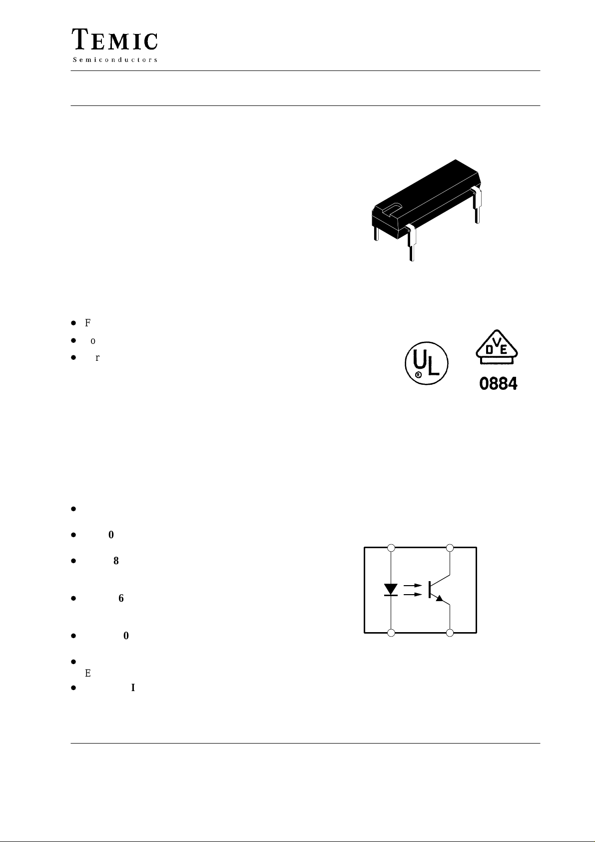
Description
The CNY21N consists of a phototransistor optically
coupled to a gallium arsenide infrared emitting diode in
a 4-lead plastic dual inline package.
The single components are mounted on one leadframe in
the opposite position, providing a fixed distance between
input and output for highest safety requirements of
> 3 mm.
Application
Circuits for safe protective separation against electrical
shock according to safety class II (reinforced isolation):
D
For application class I - IV at mains voltage ≤ 300 V
D
For application class I - IV at mains voltage ≤ 600 V
CNY21N
95 10533
D
For application class I - III at mains voltage ≤ 1000 V
according, to VDE 0884, table 2, suitable for:
Switch-mode power supplies, computer peripheral
interface, microprocessor system interface, line
receiver.
These couplers perform safety functions according to the following equipment standards:
D
VDE 0884
Optocoupler providing protective separation
D
VDE 0804
Telecommunication apparatus and data processing
D
VDE 0805/IEC 950/EN 60950
Office machines (applied for reinforced isolation for
mains voltage ≤ 400 V
D
VDE 0860/lEC 65
Safety for mains operated electronic and related
household apparatus
D
VDE 0700/IEC 335
Household equipment
D
VDE 0160
Electronic equipment for electrical power installation
D
VDE 0750/IEC 601
Medical equipment
RMS
)
Pin Connection
A (+)
C (–)
C
95 10850
E
TELEFUNKEN Semiconductors
Rev . A1, 11-Jun-96
1 (10)
CNY21N
Features
According to VDE 0884
D
Rated impulse voltage (transient overvoltage)
= 8 kV peak
V
IOTM
D
Isolation test voltage (partial discharge test voltage)
= 2.8 kV peak
V
pd
D
Rated isolation voltage (RMS includes DC)
IOWM
IORM
= 1000 V
= 1000 V
V
D
Rated recurring peak voltage (repetitive)
V
D
Creeping current resistance according to
VDE 0303/IEC 112
Comparative Tracking Index: CTI = 275
Absolute Maximum Ratings
(1450 V peak)
RMS
RMS
D
Thickness through insulation > 3 mm
D
Isolation materials according to UL 94
D
Pollution degree 2 (DIN/VDE 0110)
D
Climatic classification 55/085/21 (IEC 68 part 1)
D
Further approvals: BS 415, BS 7002, SETI: IEC 950,
UL 1577: File no: E 76222
D
Special construction: therefore extra low coupling
capacity of typical 0.3 pF, high Common Mode
Rejection
D
Low temperature coefficient of CTR
D
Current Transfer Ratio (CTR) of typical 60%
Input (Emitter)
Parameters Test Conditions Symbol Value Unit
Reverse voltage V
Forward current I
Forward surge current tp ≤ 10 ms I
Power dissipation T
≤ 25°C P
amb
Junction temperature T
Output (Detector)
Parameters Test Conditions Symbol Value Unit
Collector emitter voltage V
Emitter collector voltage V
Collector current I
Collector peak current tp/T = 0.5, tp ≤ 10 ms I
Power dissipation T
≤ 25°C P
amb
Junction temperature T
Coupler
Parameters Test Conditions Symbol Value Unit
AC isolation test voltage (RMS) V
Total power dissipation T
Ambient temperature range T
Storage temperature range T
Soldering temperature 2 mm from case t ≤ 10 s T
≤ 25°C P
amb
R
F
FSM
tot
CEO
ECO
C
CM
tot
IO
tot
amb
stg
sd
5 V
50 mA
1.5 A
120 mW
j
100 °C
32 V
5 V
50 mA
100 mA
130 mW
j
100 °C
8.2 kV
250 mW
–55 to +85 °C
–55 to +100 °C
260 °C
2 (10)
TELEFUNKEN Semiconductors
Rev . A1, 11-Jun-96
1)
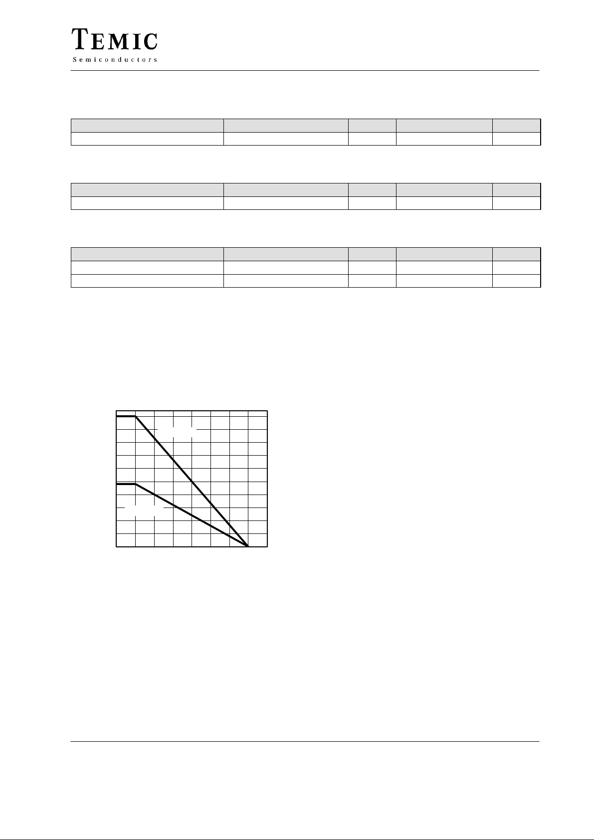
Maximum Safety Ratings
(according to VDE 0884)
Input (Emitter)
Parameters Test Conditions Symbol Value Unit
Forward current I
Output (Detector)
Parameters Test Conditions Symbol Value Unit
Power dissipation T
≤ 25°C P
amb
Coupler
Parameters Test Conditions Symbol Value Unit
Rated impulse voltage V
Safety temperature T
si
si
IOTM
si
CNY21N
120 mA
250 mW
8 kV
180 °C
1)
This device is used for protective separation against electrical shock only within the maximum safety ratings.
This must be ensured by using protective circuits in the applications.
Derating Diagram
250
225
200
175
150
125
mA ( mA )
100
75
Isi (mA)
50
25
0
0 25 50 75 100 125 150 175 200
Psi (mW)
T
( °C )95 10888
amb
TELEFUNKEN Semiconductors
Rev . A1, 11-Jun-96
3 (10)
 Loading...